EP1528592A2 - Procédé de gravure de parois latérales lisses dans des composés à base de III-V pour des dispositifs électro-optiques - Google Patents
Procédé de gravure de parois latérales lisses dans des composés à base de III-V pour des dispositifs électro-optiques Download PDFInfo
- Publication number
- EP1528592A2 EP1528592A2 EP04013445A EP04013445A EP1528592A2 EP 1528592 A2 EP1528592 A2 EP 1528592A2 EP 04013445 A EP04013445 A EP 04013445A EP 04013445 A EP04013445 A EP 04013445A EP 1528592 A2 EP1528592 A2 EP 1528592A2
- Authority
- EP
- European Patent Office
- Prior art keywords
- gas
- iii
- based compound
- reactor
- introducing
- Prior art date
- Legal status (The legal status is an assumption and is not a legal conclusion. Google has not performed a legal analysis and makes no representation as to the accuracy of the status listed.)
- Granted
Links
Images


Classifications
-
- H—ELECTRICITY
- H01—ELECTRIC ELEMENTS
- H01L—SEMICONDUCTOR DEVICES NOT COVERED BY CLASS H10
- H01L21/00—Processes or apparatus adapted for the manufacture or treatment of semiconductor or solid state devices or of parts thereof
- H01L21/02—Manufacture or treatment of semiconductor devices or of parts thereof
- H01L21/04—Manufacture or treatment of semiconductor devices or of parts thereof the devices having potential barriers, e.g. a PN junction, depletion layer or carrier concentration layer
- H01L21/18—Manufacture or treatment of semiconductor devices or of parts thereof the devices having potential barriers, e.g. a PN junction, depletion layer or carrier concentration layer the devices having semiconductor bodies comprising elements of Group IV of the Periodic Table or AIIIBV compounds with or without impurities, e.g. doping materials
- H01L21/30—Treatment of semiconductor bodies using processes or apparatus not provided for in groups H01L21/20 - H01L21/26
- H01L21/302—Treatment of semiconductor bodies using processes or apparatus not provided for in groups H01L21/20 - H01L21/26 to change their surface-physical characteristics or shape, e.g. etching, polishing, cutting
- H01L21/306—Chemical or electrical treatment, e.g. electrolytic etching
- H01L21/30604—Chemical etching
- H01L21/30612—Etching of AIIIBV compounds
- H01L21/30621—Vapour phase etching
Definitions
- etching of smooth sidewalls in III-V compounds is important for optical applications. Scattering loss in electro-optical devices is proportional to sidewall roughness. Hence, the performance of devices such as waveguides, microdisc resonators, photonic crystal waveguides and photonic crystal resonators depends on reduction of the sidewall roughness.
- Single mode ridge waveguides in InP and GaAs typically require dimensions on the order of 0.5 ⁇ m to maintain single mode performance as scattering losses from the waveguide surface are a large component of the propagation loss.
- Most work on etching III-V compounds such as InP for low loss waveguides has focused on CH 4 :H 2 chemistry in standard reactive ion etch (RIE) systems.
- a feature of sidewalls produced in standard RIE systems is that the sidewalls are sloped.
- Some electro-optical devices require highly vertical sidewall geometries for improved device performance. For example, in photonic crystal lattices, it is important to provide highly vertical sidewall geometries to enable large photonic bandgaps for device performance. Hence, it is desirable to have etch chemistries that enable highly vertical sidewall geometries with smooth sidewalls.
- ICP etch systems typically produce a higher degree of vertical etches for most materials due to the increase in density of active species.
- the chemistry selection still plays an important role in obtaining high aspect ratio etching.
- a CH 4 :H 2 based chemistry is used for etching InP ; however, CH 4 :H 2 based chemistry has difficulty etching very high apect ratios..
- Using chlorine based chemistry is problematic for obtaining high aspect ratio etching due to the highly reactive nature of chlorine.
- Mirkarimi see Attorney Docket No. 10030753
- Mirkarimi has shown the usefulness of using HBr:CH 4 :H 2 chemistry to achieve deep etching in III-V compounds.
- the sidewalls of the etched III-V structure in some quaternary compositions such as InGaAsP exhibit rough sidewalls when using Hbr:CH 4 :H 2 chemistry.
- BCl 3 additions chemistry is used to provide high aspect ratio etching together with smooth sidewalls.
- the BCl 3 additions improve the smoothness of the etched sidewalls and other surfaces.
- Optical losses on narrow waveguides have been typically reduced by a factor of 10 through the BCl 3 additions and typical etch rates of 370 nm/min can be achieved compared to etch rates of 35 nm/min using standard CH 4 :H 2 based chemistry.
- appropriate mask layer 120 typically SiO 2 or Si 3 N 4 is grown onto III-V epitaxial layer 110 or onto III-V substrate 105 of sample 100.
- Layer 130 is either photoresist or e-beam resist.
- Typical III-V materials are those that are combinations of Group III elements such as A1, Ga, In and B and Group V elements such as N, P, As and Sb.
- the use of SiO 2 or Si 3 N 4 mask 120 or other similar mask material offers etch selectivity between the mask material and the III-V material.
- the etch rate ratio of InP/SiO2 ranges from 20-50 depending on the etch conditions which is quite large.
- mask layer 120 is defined by lithographic techniques such as direct write electron beam, standard contact lithography or other lithography appropriate for the desired feature size typically on the order of 1 ⁇ m on layer 130.
- the desired etch pattern is transferred into mask layer 120 using a dry etch technique such as CHF 3 in an RIE system.
- Sample 100 is then etched using either an RIE or inductively coupled plasma (ICP) system yielding a high aspect ratio structure with smooth sidewalls 115.
- photoresist layer 130 is removed using a solvent bath followed by a high pressure (400mTorr) 02 plasma clean.
- chemistries involving CH 4 , H 2 , HBr and BCl 3 are then used to transfer the lithographically defined features into III-V layer 110 or III-V substrate 105.
- the chemistries involving CH 4 , H 2 , HBr and BCl 3 provide the desired smooth etch by forming a passivation layer on sidewalls 150.
- the smoothness of sidewalls 150 in FIG. 1 may be estimated from scanning electron microscopy which then influences the propagation loss measurements.
- HI or IBr or some combination of group VII gaseous species (Br, F, I) may be substituted for HBr.
- the iodine (I) will typically behave similarly with the bromine (Br) and form a lower volatility salt with indium (In) compared to, for example, chlorine (C1) and again form a passivation layer on sidewalls 150.
- BCl 3 may be used with H 2 and CH 4 such that the ratio of CH 4 to H 2 is greater than 1:1, for example 2:1, respectively.
- the etch chemistry is typically a combination of HBr:CH 4 :H 2 :BCl 3 .
- the ratio of HBr:CH 4 :H 2 is set to about 30:5:5 while BCl 3 may be adjusted up to about 50% by volume.
- ICP instead of RIE typically enhances the smoothness although, typically, significant reductions of surface roughness are achievable using RIE alone.
- the ratio of HBr:CH 4 :H 2 is set to about 30:5:5 while BCl 3 is typically adjusted to about 33% by volume.
- BCl 3 is typically adjusted to about 33% by volume.
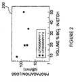
- propagation loss is significantly reduced for this embodiment along with the surface roughness of sidewalls 115. From graph 200 in FIG. 2, it is apparent that as the concentration of BCl 3 approaches about 33% by volume the propagation loss decreases, as the concentration of BCl 3 exceeds about 33% by volume the propagation loss increases as a consequence of increased surface roughness of sidewalls 115.
- typical values for reactor 305 in accordance with the invention are having radio frequency (RF) generator 310 typically operating at about 13.56 mHz and in the range 0-200 watts while having RF generator 320 typically operating at about 2 mHz and in the range 50-800 watts with reactor 305 at a pressure typically in the range 2-20 mTorr.
- Sample 100 is placed on heater 350.
- the temperature was set to 60°C although it is expected that the actual temperature may be higher during the etch. The temperature setting is determined by the material being etched and may be higher or lower for the other III-V materials under investigation.
- FIG. 4a shows an electron micrograph of sidewalls 115 using RF generator 310 only resulting in a pure RIE etch.
- the ratio of BCl 3 :HBr:H 2 :CH 4 is set at 3:32:4:4 and BCl 3 is set at 7% by volume.
- FIG. 4b shows an electron micrograph of significantly smoother sidewalls 115 when using reactor 305 with ICP mode included so that both RF generator 310 and RF generator 320 are in use.
- the ratio of BCl 3 :HBr:H 2 :CH 4 is set at 3:32:4:4 and BCl 3 is set at 7% by volume.
- RF 310 is typically set at about 100 watts while RF 320 is typically set at about 400 watts at a typical pressure of about 5 mTorr in reactor 305.
- the effective DC bias lies at about 350 volts.
- this DC bias value may be too high causing etch damage due to the highly energized incoming ions.
- the DC bias is typically reduced by reducing RF 1 310 to values under 75 watts. Reduction in RF 1 reduces the DC bias while preserving the smooth sidewall structure.
Landscapes
- Engineering & Computer Science (AREA)
- General Physics & Mathematics (AREA)
- General Chemical & Material Sciences (AREA)
- Physics & Mathematics (AREA)
- Chemical Kinetics & Catalysis (AREA)
- Condensed Matter Physics & Semiconductors (AREA)
- Chemical & Material Sciences (AREA)
- Manufacturing & Machinery (AREA)
- Computer Hardware Design (AREA)
- Microelectronics & Electronic Packaging (AREA)
- Power Engineering (AREA)
- Drying Of Semiconductors (AREA)
- ing And Chemical Polishing (AREA)
Applications Claiming Priority (2)
| Application Number | Priority Date | Filing Date | Title |
|---|---|---|---|
| US10/692,772 US7196017B2 (en) | 2003-10-24 | 2003-10-24 | Method for etching smooth sidewalls in III-V based compounds for electro-optical devices |
| US692772 | 2003-10-24 |
Publications (3)
| Publication Number | Publication Date |
|---|---|
| EP1528592A2 true EP1528592A2 (fr) | 2005-05-04 |
| EP1528592A3 EP1528592A3 (fr) | 2006-01-11 |
| EP1528592B1 EP1528592B1 (fr) | 2008-05-28 |
Family
ID=34423325
Family Applications (1)
| Application Number | Title | Priority Date | Filing Date |
|---|---|---|---|
| EP04013445A Expired - Lifetime EP1528592B1 (fr) | 2003-10-24 | 2004-06-08 | Procédé de gravure de parois latérales lisses dans des composés à base de III-V pour des dispositifs électro-optiques |
Country Status (6)
| Country | Link |
|---|---|
| US (1) | US7196017B2 (fr) |
| EP (1) | EP1528592B1 (fr) |
| JP (1) | JP2005129943A (fr) |
| CN (1) | CN1609712B (fr) |
| DE (1) | DE602004014085D1 (fr) |
| SG (1) | SG111214A1 (fr) |
Cited By (1)
| Publication number | Priority date | Publication date | Assignee | Title |
|---|---|---|---|---|
| EP1557874A3 (fr) * | 2004-01-26 | 2006-03-15 | Agilent Technologies, Inc. | Procédé de gravure d'éléments semi-conducteurs à haut facteur de forme dans des composés à base de III-V pour des dispositifs optoélectroniques |
Families Citing this family (6)
| Publication number | Priority date | Publication date | Assignee | Title |
|---|---|---|---|---|
| US8298958B2 (en) * | 2008-07-17 | 2012-10-30 | Lam Research Corporation | Organic line width roughness with H2 plasma treatment |
| JP5048611B2 (ja) * | 2008-08-05 | 2012-10-17 | 株式会社アルバック | 半導体装置の製造装置及び半導体装置の製造方法 |
| KR101498676B1 (ko) | 2008-09-30 | 2015-03-09 | 삼성전자주식회사 | 3차원 반도체 장치 |
| JP5813400B2 (ja) * | 2011-07-26 | 2015-11-17 | 株式会社アルバック | ドライエッチング方法 |
| US9484216B1 (en) | 2015-06-02 | 2016-11-01 | Sandia Corporation | Methods for dry etching semiconductor devices |
| CN113808936A (zh) * | 2021-09-14 | 2021-12-17 | 苏州长瑞光电有限公司 | 刻蚀方法,半导体器件制造方法及半导体器件 |
Family Cites Families (6)
| Publication number | Priority date | Publication date | Assignee | Title |
|---|---|---|---|---|
| US5338394A (en) | 1992-05-01 | 1994-08-16 | Alliedsignal Inc. | Method for etching indium based III-V compound semiconductors |
| US5624529A (en) * | 1995-05-10 | 1997-04-29 | Sandia Corporation | Dry etching method for compound semiconductors |
| GB9616225D0 (en) * | 1996-08-01 | 1996-09-11 | Surface Tech Sys Ltd | Method of surface treatment of semiconductor substrates |
| US6034344A (en) * | 1997-12-19 | 2000-03-07 | United Technologies Corp. | Method for applying material to a face of a flow directing assembly for a gas turbine engine |
| US6635185B2 (en) * | 1997-12-31 | 2003-10-21 | Alliedsignal Inc. | Method of etching and cleaning using fluorinated carbonyl compounds |
| TW586155B (en) | 2001-07-19 | 2004-05-01 | Matsushita Electric Ind Co Ltd | Dry etching method and apparatus |
-
2003
- 2003-10-24 US US10/692,772 patent/US7196017B2/en not_active Expired - Fee Related
-
2004
- 2004-06-08 DE DE602004014085T patent/DE602004014085D1/de not_active Expired - Fee Related
- 2004-06-08 EP EP04013445A patent/EP1528592B1/fr not_active Expired - Lifetime
- 2004-10-05 SG SG200405689A patent/SG111214A1/en unknown
- 2004-10-20 JP JP2004305978A patent/JP2005129943A/ja active Pending
- 2004-10-25 CN CN200410086335.6A patent/CN1609712B/zh not_active Expired - Fee Related
Cited By (1)
| Publication number | Priority date | Publication date | Assignee | Title |
|---|---|---|---|---|
| EP1557874A3 (fr) * | 2004-01-26 | 2006-03-15 | Agilent Technologies, Inc. | Procédé de gravure d'éléments semi-conducteurs à haut facteur de forme dans des composés à base de III-V pour des dispositifs optoélectroniques |
Also Published As
| Publication number | Publication date |
|---|---|
| JP2005129943A (ja) | 2005-05-19 |
| CN1609712A (zh) | 2005-04-27 |
| CN1609712B (zh) | 2010-11-03 |
| EP1528592A3 (fr) | 2006-01-11 |
| US20050090116A1 (en) | 2005-04-28 |
| EP1528592B1 (fr) | 2008-05-28 |
| SG111214A1 (en) | 2005-05-30 |
| US7196017B2 (en) | 2007-03-27 |
| DE602004014085D1 (de) | 2008-07-10 |
Similar Documents
| Publication | Publication Date | Title |
|---|---|---|
| Volatier et al. | Extremely high aspect ratio GaAs and GaAs/AlGaAs nanowaveguides fabricated using chlorine ICP etchingwith N2-promoted passivation | |
| JPH0221651B2 (fr) | ||
| Rommel et al. | Effect of H 2 on the etch profile of InP/InGaAsP alloys in Cl 2/Ar/H 2 inductively coupled plasma reactive ion etching chemistries for photonic device fabrication | |
| Jun et al. | Deep anisotropic LiNbO3 etching with SF6/Ar inductively coupled plasmas | |
| Bouchoule et al. | Sidewall passivation assisted by a silicon coverplate during Cl2–H2 and HBr inductively coupled plasma etching of InP for photonic devices | |
| EP1528592B1 (fr) | Procédé de gravure de parois latérales lisses dans des composés à base de III-V pour des dispositifs électro-optiques | |
| Guilet et al. | Optimization of a Cl2–H2 inductively coupled plasma etching process adapted to nonthermalized InP wafers for the realization of deep ridge heterostructures | |
| Li et al. | Dry-etch of As2S3 thin films for optical waveguide fabrication | |
| Park et al. | InGaAsP-InP nanoscale waveguide-coupled microring lasers with submilliampere threshold current using Cl/sub 2/--N/sub 2/-based high-density plasma etching | |
| US20010025826A1 (en) | Dense-plasma etching of InP-based materials using chlorine and nitrogen | |
| Wüest et al. | Fabrication of a hard mask for InP based photonic crystals: Increasing the plasma-etch selectivity of poly (methyl methacrylate) versus SiO2 and SiNx | |
| Bouchoule et al. | Anisotropic and smooth inductively coupled plasma etching of III-V laser waveguides using HBr-O2 chemistry | |
| Sultana et al. | HBr based inductively coupled plasma etching of high aspect ratio nanoscale trenches in InP: considerations for photonic applications | |
| Chien et al. | Controlling the etch selectivity of silicon using low-RF power HBr reactive ion etching | |
| Constantine et al. | Etching of GaAs/AlGaAs rib waveguide structures using BCl3/Cl2/N2/Ar electron cyclotron resonance | |
| JP2010040780A (ja) | 半導体装置およびその製造方法、並びにプラズマエッチング装置 | |
| Hatate et al. | Fabrication of InP submicron pillars for two-dimensional photonic crystals by reactive ion etching | |
| Lu et al. | Inductively coupled plasma etching of GaAs low loss waveguides for a traveling waveguide polarization converter, using chlorine chemistry | |
| EP1557874A2 (fr) | Procédé de gravure d'éléments semi-conducteurs à haut facteur de forme dans des composés à base de III-V pour des dispositifs optoélectroniques | |
| Piotrowska et al. | Application of CCl2F2-and CCl4-based plasmas for RIE of GaSb and related materials | |
| JP2710545B2 (ja) | 埋め込み型ヘテロ構造レーザの製造方法 | |
| Goodyear et al. | A Comparison of Production Plasma Etch Chemistries for InP and Related Materials. | |
| Kobayashi et al. | Recent progress of photonic devices using clean and fine dry processes | |
| Bouchoule et al. | Processing of InP-based shallow ridge laser waveguides using a HBr ICP plasma | |
| Deichsel et al. | Fabrication of dry etched and subsequently passivated laser facets in GaAs∕ AlGaAs |
Legal Events
| Date | Code | Title | Description |
|---|---|---|---|
| PUAI | Public reference made under article 153(3) epc to a published international application that has entered the european phase |
Free format text: ORIGINAL CODE: 0009012 |
|
| AK | Designated contracting states |
Kind code of ref document: A2 Designated state(s): AT BE BG CH CY CZ DE DK EE ES FI FR GB GR HU IE IT LI LU MC NL PL PT RO SE SI SK TR |
|
| AX | Request for extension of the european patent |
Extension state: AL HR LT LV MK |
|
| PUAL | Search report despatched |
Free format text: ORIGINAL CODE: 0009013 |
|
| AK | Designated contracting states |
Kind code of ref document: A3 Designated state(s): AT BE BG CH CY CZ DE DK EE ES FI FR GB GR HU IE IT LI LU MC NL PL PT RO SE SI SK TR |
|
| AX | Request for extension of the european patent |
Extension state: AL HR LT LV MK |
|
| 17P | Request for examination filed |
Effective date: 20060215 |
|
| AKX | Designation fees paid |
Designated state(s): DE FR GB |
|
| RAP1 | Party data changed (applicant data changed or rights of an application transferred) |
Owner name: AVAGO TECHNOLOGIES FIBER IP (SINGAPORE) PTE. LTD. |
|
| GRAP | Despatch of communication of intention to grant a patent |
Free format text: ORIGINAL CODE: EPIDOSNIGR1 |
|
| GRAS | Grant fee paid |
Free format text: ORIGINAL CODE: EPIDOSNIGR3 |
|
| GRAA | (expected) grant |
Free format text: ORIGINAL CODE: 0009210 |
|
| AK | Designated contracting states |
Kind code of ref document: B1 Designated state(s): DE FR GB |
|
| REG | Reference to a national code |
Ref country code: GB Ref legal event code: FG4D |
|
| REF | Corresponds to: |
Ref document number: 602004014085 Country of ref document: DE Date of ref document: 20080710 Kind code of ref document: P |
|
| PLBE | No opposition filed within time limit |
Free format text: ORIGINAL CODE: 0009261 |
|
| STAA | Information on the status of an ep patent application or granted ep patent |
Free format text: STATUS: NO OPPOSITION FILED WITHIN TIME LIMIT |
|
| PG25 | Lapsed in a contracting state [announced via postgrant information from national office to epo] |
Ref country code: DE Free format text: LAPSE BECAUSE OF NON-PAYMENT OF DUE FEES Effective date: 20090101 |
|
| 26N | No opposition filed |
Effective date: 20090303 |
|
| REG | Reference to a national code |
Ref country code: FR Ref legal event code: ST Effective date: 20110729 |
|
| PG25 | Lapsed in a contracting state [announced via postgrant information from national office to epo] |
Ref country code: FR Free format text: LAPSE BECAUSE OF NON-PAYMENT OF DUE FEES Effective date: 20080728 |
|
| PGFP | Annual fee paid to national office [announced via postgrant information from national office to epo] |
Ref country code: GB Payment date: 20130605 Year of fee payment: 10 |
|
| REG | Reference to a national code |
Ref country code: GB Ref legal event code: 732E Free format text: REGISTERED BETWEEN 20130725 AND 20130731 |
|
| GBPC | Gb: european patent ceased through non-payment of renewal fee |
Effective date: 20140608 |
|
| PG25 | Lapsed in a contracting state [announced via postgrant information from national office to epo] |
Ref country code: GB Free format text: LAPSE BECAUSE OF NON-PAYMENT OF DUE FEES Effective date: 20140608 |