EP1528543B1 - Optical disk apparatus - Google Patents
Optical disk apparatus Download PDFInfo
- Publication number
- EP1528543B1 EP1528543B1 EP04024986A EP04024986A EP1528543B1 EP 1528543 B1 EP1528543 B1 EP 1528543B1 EP 04024986 A EP04024986 A EP 04024986A EP 04024986 A EP04024986 A EP 04024986A EP 1528543 B1 EP1528543 B1 EP 1528543B1
- Authority
- EP
- European Patent Office
- Prior art keywords
- sampling
- signal
- sample
- circuit
- spot
- Prior art date
- Legal status (The legal status is an assumption and is not a legal conclusion. Google has not performed a legal analysis and makes no representation as to the accuracy of the status listed.)
- Expired - Fee Related
Links
Images


Classifications
-
- G—PHYSICS
- G11—INFORMATION STORAGE
- G11B—INFORMATION STORAGE BASED ON RELATIVE MOVEMENT BETWEEN RECORD CARRIER AND TRANSDUCER
- G11B7/00—Recording or reproducing by optical means, e.g. recording using a thermal beam of optical radiation by modifying optical properties or the physical structure, reproducing using an optical beam at lower power by sensing optical properties; Record carriers therefor
- G11B7/08—Disposition or mounting of heads or light sources relatively to record carriers
- G11B7/09—Disposition or mounting of heads or light sources relatively to record carriers with provision for moving the light beam or focus plane for the purpose of maintaining alignment of the light beam relative to the record carrier during transducing operation, e.g. to compensate for surface irregularities of the latter or for track following
-
- G—PHYSICS
- G11—INFORMATION STORAGE
- G11B—INFORMATION STORAGE BASED ON RELATIVE MOVEMENT BETWEEN RECORD CARRIER AND TRANSDUCER
- G11B7/00—Recording or reproducing by optical means, e.g. recording using a thermal beam of optical radiation by modifying optical properties or the physical structure, reproducing using an optical beam at lower power by sensing optical properties; Record carriers therefor
- G11B7/004—Recording, reproducing or erasing methods; Read, write or erase circuits therefor
- G11B7/0045—Recording
-
- G—PHYSICS
- G11—INFORMATION STORAGE
- G11B—INFORMATION STORAGE BASED ON RELATIVE MOVEMENT BETWEEN RECORD CARRIER AND TRANSDUCER
- G11B7/00—Recording or reproducing by optical means, e.g. recording using a thermal beam of optical radiation by modifying optical properties or the physical structure, reproducing using an optical beam at lower power by sensing optical properties; Record carriers therefor
- G11B7/08—Disposition or mounting of heads or light sources relatively to record carriers
- G11B7/09—Disposition or mounting of heads or light sources relatively to record carriers with provision for moving the light beam or focus plane for the purpose of maintaining alignment of the light beam relative to the record carrier during transducing operation, e.g. to compensate for surface irregularities of the latter or for track following
- G11B7/0901—Disposition or mounting of heads or light sources relatively to record carriers with provision for moving the light beam or focus plane for the purpose of maintaining alignment of the light beam relative to the record carrier during transducing operation, e.g. to compensate for surface irregularities of the latter or for track following for track following only
- G11B7/0903—Multi-beam tracking systems
-
- G—PHYSICS
- G11—INFORMATION STORAGE
- G11B—INFORMATION STORAGE BASED ON RELATIVE MOVEMENT BETWEEN RECORD CARRIER AND TRANSDUCER
- G11B7/00—Recording or reproducing by optical means, e.g. recording using a thermal beam of optical radiation by modifying optical properties or the physical structure, reproducing using an optical beam at lower power by sensing optical properties; Record carriers therefor
- G11B7/12—Heads, e.g. forming of the optical beam spot or modulation of the optical beam
- G11B7/125—Optical beam sources therefor, e.g. laser control circuitry specially adapted for optical storage devices; Modulators, e.g. means for controlling the size or intensity of optical spots or optical traces
- G11B7/126—Circuits, methods or arrangements for laser control or stabilisation
- G11B7/1263—Power control during transducing, e.g. by monitoring
-
- G—PHYSICS
- G11—INFORMATION STORAGE
- G11B—INFORMATION STORAGE BASED ON RELATIVE MOVEMENT BETWEEN RECORD CARRIER AND TRANSDUCER
- G11B7/00—Recording or reproducing by optical means, e.g. recording using a thermal beam of optical radiation by modifying optical properties or the physical structure, reproducing using an optical beam at lower power by sensing optical properties; Record carriers therefor
- G11B7/12—Heads, e.g. forming of the optical beam spot or modulation of the optical beam
- G11B7/13—Optical detectors therefor
- G11B7/131—Arrangement of detectors in a multiple array
Definitions
- the present invention relates to an optical disk apparatus for recording onto optical disks such as CD-R (compact disk recordable) and DVD-R (digital versatile disk recordable), and, in particular, to sampling and holding of a photoelectrically converted signal in an optical pickup.
- optical disks such as CD-R (compact disk recordable) and DVD-R (digital versatile disk recordable)
- a photoelectrically converted signal which is obtained by a built-in photo-detector circuit in an optical pickup and which corresponds to a semiconductor laser beam reflected by a disk at recording time, has the waveform shown in Fig. 5A .
- the photoelectrically converted signal is normally transmitted to an RF signal processing circuit through a flexible cable. This is disclosed in, for example, Japanese Unexamined Patent Application Publication No. 11-53735 (page 5, Fig. 1 ).
- the RF signal processing circuit calculates signals, such as a servo signal and an APC (automatic emitting-power control circuit) control signal, based on the photoelectrically converted signal input through the flexible cable.
- the photoelectrically converted signal must be sampled in periods (the low level periods shown in Fig. 5A ) in which the semiconductor laser beam is emitted at a bias power.
- An increase in recording speed shortens the sampling period.
- a signal settling time which is obtained when a photoelectrically converted signal in the recording period changes to the photoelectrically converted signal in bias periods (the low level periods shown in Fig. 5A ), must be reduced.
- the above flexible cable electrically acts as a distributed parameter line and has a frequency characteristic having a peak in the vicinity of 150 MHz. Therefore, if the slew rate of an output from the photo-detector circuit is enhanced in order to shorten the settling time, as Fig. 5B shows, ringing 50, which occurs at a bias power portion of the photoelectrically converted signal in the bias period (low level period), only increases. Conversely, the settling time lengthens.
- enhancing the slew rate represents short-time charging for a capacitive element in the flexible cable and a load capacitance such as an input capacitance of the RF signal processing circuit at a post stage
- a circuit current flowing at a final stage of the photo-detector circuit must be increased. This increases the power consumption, and the increased power often exceeds the allowable value in a package. Accordingly, also in this sense, the settling time cannot be shortened. Therefore, it is very difficult to shorten the settling time from the recording power level to the bias power level from the order of ten nanoseconds. This results in the inability to cope with increased recording speed, thus decreasing the servo accuracy. In some cases, tracking servo control is impossible.
- a sample-and-hold circuit in the photo-detector circuit by providing a sample-and-hold circuit in the photo-detector circuit, and sampling and holding the photoelectrically converted signal before performing transmission through the flexible cable, a sampled-and-held signal having a small amplitude is transmitted through the flexible cable.
- This causes the signal transmitted through the flexible cable to have no large change in level. Accordingly, the need for a circuit having a large slew rate is eliminated.
- a circuit including a hold capacitor whose capacitance is large is not required (up to 11T of 1 ⁇ CD, that is, approximately 100 kHz) as the sample-and-hold circuit.
- no large current is required as a driving current in a current-voltage converting circuit at a previous stage.
- a slew rate at an initial stage can be sufficiently enhanced, thus shortening a signal settling time.
- High speed recording has a high clock frequency.
- the clock frequency is approximately 400 MHz.
- 3T bias power emitting interval
- 4T the photoelectrically converted signal
- Push-pull methods and three-beam methods have conventionally been employed as tracking servo methods for apparatuses for recording on or playing back optical disks.
- typical one is a differential push-pull method.
- Fig. 6 The principle of the differential push-pull method is shown in Fig. 6 .
- three beam spots (a main spot M and side spots S1 and S2) formed by a diffraction grating are positioned so that the side spots S1 and S2 are disk-radially shifted with respect to the main spot M by half of a track pitch P.
- Reflected beams from the main spot M and both side spots S1 and S2 are photoelectrically converted by photo-detectors so that push-pull signals can be obtained for the spots M, S1, and S2.
- the photoelectrically converted signals corresponding to the spots M, S1, and S2 must be sampled in the above-described manner.
- the photoelectrically converted signal corresponding to the main spot M when considering detection of an address signal, sampling must be performed within a 3T space, which is the shortest repetition. For the photoelectrically converted signal corresponding to each side spot, only a servo signal needs to be detected. Thus, originally, it is preferable to perform signal detection concerning a signal having 6T or longer.
- a circuit for the side spot when the main spot output and each side spot output are sampled with the same sampling timing, also a circuit for the side spot must have a bandwidth and settling characteristic similar to those in a circuit for the main spot. The bandwidth must be extremely broadened, so that the circuit for the side spot does not sufficiently operate. Accordingly, the circuit operation is unstable. For eliminating this defect, design and circuit improvements are required. This causes problems of an increase in circuit size and an increase in production cost.
- Document JP 2001 357544 discloses an optical disc device which is configured in order to obtain a stable servo operation even if the frequency band of photodetecting signals of sub-beams are insufficient. It is proposed to receive reflected light from an optical disc by respective photodetectors. The received signals are converted, sampled and held in periods for irradiation with the recording power during a recording process. The signals are sampled and output in periods for irradiation with non-recording power. DC components of the photodetecting signals are extracted and amplified by a variable amplifier, wherein the amplification factor meets the ratio of the average power for the irradiation and the non-recording power in recording. The signals are output without amplification in the reproducing process. A differential amplifier is used to form servo error signals in accordance with the respectively outputted signals. In another embodiment the signals corresponding to the side spots are low pass filtered or sampled and held, depending on the recording speed.
- Document JP 2003 178481 discloses an optical disc device and an optical head device, wherein the servo of laser light quantity or an objective lens can have a high reliable performance. This is achieved by enabling a high-speed sample/hold process without being affected by stray capacitances on a data transmission line. Separate switching signals generated on the main circuit board are transmitted to the sample and hold circuits provided for laser servo and for tracking/focusing servo.
- the present invention has been made in view of the above circumstances. It is an object of the present invention to provide an optical disk apparatus in which, by only transmitting a sampling-timing signal for a main spot, a photoelectrically converted signal for a side spot is sampled and held to enable reduced flexible cable size, and in which a circuit for the side spot has a narrower band characteristic and a longer settling characteristic compared with a circuit for the main spot.
- optical disc apparatus according to independent claim 1.
- Preferred embodiments of the optical disc apparatus are defined in the respective dependent claims.
- the above object has been achieved by provision of an optical disk apparatus for obtaining a plurality of servo signals by separating a laser beam into at least two beams, converging the at least two beams on a first spot and at least one second spot on a recording medium, and photoelectrically converting reflected beams from the first spot and the at least one second spot at the time of recording data on the recording medium.
- the optical disk apparatus includes a first converting unit for converting the reflected beam from the first spot into an electrical signal, a first sample-and-hold unit for sampling and holding the electrical signal obtained by the first converting unit, a second converting unit for converting the reflected beam from the at least one second spot into an electrical signal, a second sample-and-hold unit for sampling and holding the electrical signal obtained by the second converting unit, a signal generating unit for generating, based on a given first sampling-timing signal for determining sampling timing for the first sample-and-hold unit, a second sampling-timing signal for determining sampling timing for the second sample-and-hold unit, and a transmitting unit for transmitting, to signal processing circuits at a subsequent stage, sampled-and-held signals obtained by the first and second sample-and-hold unit.
- wiring for sending the second sampling-timing signal can be omitted to enable reduction in flexible cable size, so that reduction in apparatus size can be achieved.
- the bandwidth of the second converting means can be narrowed than that of the first converting means, and the settling characteristic of the second converting means can be lengthened. This enables an optimal and inexpensive circuit to be used for the side spot.
- Fig. 1 is a block diagram showing an optical disk apparatus according to an embodiment of the present invention.
- the optical disk apparatus includes an objective lens 1, a beam splitter (BS) 2, converging lenses 3 and 4, a semiconductor laser (LD) 5, a laser driving circuit (LDD) for driving the semiconductor laser 5, a photo-detector circuit (PDIC) 7, a front-monitor photo-detector circuit (FPDIC) 8, an RF signal processing circuit 9, a digital signal processor (DSP) 10, and a controller 11.
- BS beam splitter
- LDD laser driving circuit
- PDIC photo-detector circuit
- FPDIC front-monitor photo-detector circuit
- DSP digital signal processor
- the photo-detector circuit 7 includes a photo-detector (PD) 71, a current-voltage converter (I/V) 72, and sample-and-hold circuits (S/H) 73 and 74.
- the front-monitor detector circuit 8 includes a photo-detector (PD) 81, and a current-voltage converter (I/V) 82, and sample-and-hold circuits (S/H) 83 and 84.
- the RF signal processing circuit 9 includes an optical photo coupler (OPC) 91, a wobble address detecting circuit (indicated by "WOBBLE ADDRESS”) 92, a servo-signal generating circuit (indicated by "SERVO”) 93, an RF signal generating circuit (indicated by "RF”) 94, and an automatic emitting-power control circuit (APC) 95.
- the digital signal processor 10 includes a servo circuit 101, a signal processing circuit 102, a decoder 103, a write-strategy timing-generating circuit 104, and an encoder 105.
- the RF signal processing circuit 9 corresponds to a signal processing means in the appended claims.
- Fig. 2 is a detailed block diagram showing the photo-detector circuit 7 shown in Fig. 1 .
- the photo-detector 71 has photo-receiving areas A to H for receiving portions of a main spot M and side spots S1 and S2. Signals which are obtained such that reflected beams are converted into corresponding currents in the photo-receiving areas A to H are converted into voltage signals by current-voltage conversion units.
- typical current-voltage conversion units 72D and 72G are only shown. The photoelectrically converted signals are sampled and held by sample-and-hold circuits 73D, 74D, and 74G.
- circuits corresponding to the photo-receiving areas there are circuits corresponding to the photo-receiving areas. Accordingly, the number of configurations as shown in Fig. 2 is four for the main spot, and the number of configurations as shown in Fig. 2 is four for the side spots. Therefore, there are eight current-voltage converters 72A to 72H, four sample-and-hold circuits 73A to 73D, and eight sample-and-hold circuits 74A to 74H.
- the photo-receiving areas A to H of the photo-detector 71, and the current-voltage converters 72A, 72B, 72C, and 72D correspond to a first converting means in the appended claims.
- the sample-and-hold circuits 74A, 74B, 74C, and 74D correspond to a first sample-and-hold means in the appended claims.
- the areas E, F, G, and H of the photo-detector 71, and the current-voltage converters 72E, 72F, 72G (only this is shown in Fig. 2 ), and 72H correspond to a second converting means in the appended claims.
- the sample-and-hold circuits 74E, 74F, 74G (only this is shown in Fig. 2 ), and 74H correspond to a second sample-and-hold means in the appended claims.
- the main spot M shown in Fig. 6 corresponds to a first spot in the appended claims.
- the side spots S1 and S2 shown in Fig. 6 correspond to at least one second spot in the appended claims.
- the controller 11 outputs write data 200 to the encoder 105.
- the encoder 105 encodes the write data 200 and outputs encoded write data 201 to the write-strategy timing-generating circuit 104.
- the write-strategy timing-generating circuit 104 generates write pulses in response to the write data 201, and outputs the generated write pulses to the laser driving circuit 6.
- the laser driving circuit 6 performs power control in response to the write pulses by using bias power output.
- the modulated laser beam is converged on an optical disk 100 through the beam splitter 2 and the objective lens 1.
- a laser beam reflected by the optical disk 100 is split into two by the beam splitter 2.
- One split beam is input to the photo-detector 71 in the photo-detector circuit 7, and the other one slit beam is input to the photo-detector 81 in the front-monitor photo-detector circuit 8.
- the photo-detector 71 in the photo-detector circuit 7 receives and converts the beam into a corresponding current.
- the current-voltage converter 72 converts the current into a voltage and outputs the voltage as photo-reception signals to the sample-and-hold circuits 73 and 74.
- the sample-and-hold circuits 73 and 74 sample and hold the photo-reception signals and transmit the photo-reception signals to the RF signal processing circuit 9 through a flexible cable (not shown).
- the photo-detector 81 in the front-monitor photo-detector circuit 8 converts the beam into a corresponding current.
- the current-voltage converter 82 converts the current into a voltage and outputs the voltage as power monitor signals to the sample-and-hold circuits 83 and 84.
- the sample-and-hold circuits 83 and 84 sample and hold the power monitor signals and transmit the signals to the RF signal processing circuit 9 through a flexible cable (not shown).
- each sample-and-hold circuit used in the photo-detector circuit 7 is described below with reference to Fig. 2 .
- the photo-detector circuit 7 has two circuit systems, that is, a main spot circuit system and a side spot circuit system. Compared with the sample-and-hold circuits 73D and 74D for the sample-and-hold circuits 73D and 74D for the main spot, the sample-and-hold circuit 74G for the side spot has a narrower bandwidth and its settling characteristic is designed to be longer.
- the photo-detector circuit 7 Based on a sampling-timing signal 302 for the main spot which is generated by the write-strategy timing-generating circuit 104, the photo-detector circuit 7 generates a sampling-timing signal for operating the sample-and-hold circuit 74G for the side spot.
- Fig. 3 is a block diagram showing a circuit that generates a sampling-timing signal 350 for the side spot circuit system based on the sampling-timing signal 302.
- a sample-timing generating circuit 60 includes a delay circuit 30, an SR flip-flop 31, and D flip-flops 32 and 33.
- the setting terminal (S) and resetting terminal (R) of the SR flip-flop 31 can respectively act to perform setting and resetting operations at rise edges.
- the resetting terminals (R) of the D flip-flops 32 and 33 can respectively act to perform resetting operations at rise edges.
- the sampling-timing signal 302 shown in Fig. 4B is originally used for sampling and holding in the main spot circuit system. Thus, it is directly input to a sample-and-hold circuit in the main spot circuit system.
- the sampling-timing signal 302 is directly input to the sample-and-hold circuit 74D in the main spot circuit system.
- the sample-and-hold circuit 74D samples low-level-period portions of the photoelectrically converted signal (corresponding to write data) in high level periods of the sampling-timing signal 302, which is input to the sample-and-hold circuit 74D.
- the sample-and-hold circuit 73D in the main spot circuit system operates based on the sampling-timing signal 301.
- the generated sampling-timing signal 350 has a narrow bandwidth and a long settling characteristic, and is adapted for the current-voltage converter 72G in the side spot circuit system.
- the sampling-timing signal 302 is input to the sample-and-hold circuit 74D and is also input to the delay circuit 30, so that the delayed signal 80 shown in Fig. 4C is generated and is input to the resetting terminal (R) of the SR flip-flop 31.
- the sampling-timing signal 302 is input to the setting terminal (S) of the SR flip-flop 31.
- the output of the inverted output terminal (xQ) of the SR flip-flop 31 is input to a data terminal (D) of the D flip-flop 32, and the sampling-timing signal 302 is input to a clock terminal (ck) and resetting terminal (R) of the D flip-flop 32.
- the clock terminal (ck) acts to operate at a rise edge.
- the resetting terminal (R) acts to operate at a fall edge.
- the output of the output terminal (Q) of the D flip-flop 32 is input to a data terminal (D) of the D flip-flop 33.
- the delayed signal 80 is input to the D flip-flop 33.
- the sampling-timing signal 302 is input to the resetting terminal (R) of the D flip-flop 33.
- the clock terminal (ck) of the D flip-flop 33 also acts to operate at a fall edge, and the resetting terminal (R) of the D flip-flop 33 acts to operate at a fall edge.
- the inverted output (xQ) of the SR flip-flop 31 is at high level. This allows the D flip-flop 32 to be operable since a high level signal is input to the data terminal (D) of the D flip-flop 32, so that the output of the output terminal (Q) is at low level.
- the D flip-flop 32 operates, and its output terminal (Q) becomes high in level, and the SR flip-flop 31 is set, so that the output of the inverted output terminal (xQ) becomes low in level.
- the output terminal (Q) of the D flip-flop 32 becomes high in level
- the data terminal (D) of the D flip-flop 33 becomes high in level. This allows the D flip-flop 33 to be operable.
- the output (similar to the sampling-timing signal 350) of the output terminal (Q) of the D flip-flop 33 is still at low level.
- the D flip-flop 33 Before the sampling-timing signal 302 rises in this state, when the delayed signal 80 changes to be in high level, as denoted by reference letter b, the D flip-flop 33 operates and its output Q becomes high in level, so that the sampling-timing signal 350 rises as denoted by reference letter c. Then, the delayed signal 80 resets the SR flip-flop 31, and the output of the inverted output terminal xQ becomes high in level. In this state, when the sampling-timing signal 302 rises in low level, the D flip-flops 32 and 33 are reset, and the output of the output terminal Q of the D flip-flop 33 becomes low in level, thus causing the sampling-timing signal 350 to fall. After all, the sampling-timing signal 350 is output with it delayed for the sampling-timing signal 302.
- sampling-timing signal 302 falls as denoted by reference letter d in Fig. 4B
- the D flip-flop 33 is reset and its output terminal Q has a low level output.
- the D flip-flop 33 does not operate and its output terminal Q remains to have a low level output, so that the sampling-timing signal 350 is not output as denoted by reference letter f in Fig. 4D .
- the sampling-timing signal 350 which is suitable for the sampling and holding operation of the sample-and-hold circuit 74G for the side spot circuit system, is generated.
- the sampling-timing generating circuit 60 shown in Fig. 3 is a circuit in which, after the sampling-timing signal 302 rises, before the sampling-timing signal 302 falls, only when the delayed signal 80 rises does the circuit output the sampling-timing signal 350.
- the sample-and-hold circuit 74G in the side spot circuit system samples and holds the above photoelectrically converted signal in the bias periods based on the sampling-timing signal 350 shown in Fig. 4D .
- the sample-and-hold circuit 74D performs a sampling and holding operation based on the sampling-timing signal 302.
- the sample-and-hold circuit 74D does not use a sampling-timing signal separately generated as described above.
- the sample-and-hold circuits 83 and 84 used in the front-monitor photo-detector circuit 8 are identical in configuration to the sample-and-hold circuit 73 used in the photo-detector circuit 7. In this case, the sample-and-hold circuits 83 and 84 have no distinction for a main spot and side spots, and are all equivalent to those for the main spot. Thus, the sample-and-hold circuits 83 and 84 perform sampling and holding operations based on the sampling-timing signals 301 and 302.
- a signal held by the sample-and-hold circuit 73 in the photo-detector circuit 7 is transmitted to the optical photo coupler (OPC) 91 and the wobble address detecting circuit 92 in the RF signal processing circuit 9 through the flexible cable.
- a signal held by the address counter 74 is transmitted to the wobble address detecting circuit 92, the servo-signal generating circuit 93, and the RF signal generating circuit 94, and the frequency characteristics and level of the read signal are shaped to generate an RF signal.
- a signal held by the sample-and-hold circuit 83 in the front-monitor photo-detector circuit 8 is transmitted to the APC 95 in the RF signal processing circuit 9, and a signal held by the adaptive filter 84 is also transmitted to the APC 95 through the flexible cable.
- the optical photo coupler (OPC) 91 in the RF signal processing circuit 9 finds an optical recording output level of the semiconductor laser 5 based on the level of the photo-reception signal in the recording period, and sets the optical recording output level in the APC 95.
- the APC 95 performs control in which, based on the level of a power monitor signal in the recording and bias periods, the emission power of the semiconductor laser 5 is used as a set value.
- the servo-signal generating circuit 93 calculates, based on a sampling signal of the photo-reception signal in the bias period, various servo signals, and outputs the calculated signals to the servo circuit 101 in the digital signal processor 10.
- the servo circuit 101 generates, based on the input servo signals, a servo signal for driving an actuator (not shown), and outputs the servo signal to the actuator. This performs tracking control and focusing control of the optical pickup including the photo-detector circuit 7, the front-monitor photo-detector circuit 8, and the optical system (the semiconductor laser 5, the beam splitter 2, the objective lens 1, etc.).
- the wobble address detecting circuit 92 Based on the sampling signals of the photo-reception signals in the recording period and the bias period, the wobble address detecting circuit 92 detects an absolute address. Based on the address, the controller 11 constantly monitors a position on the optical disk 100 at which data is currently recorded. When no data is recorded at a predetermined position, the servo circuit 101 is controlled to perform an operation such as re-recording. In addition, the controller 11 performs on-off control of the encoder 105, the spindle motor 103, and the servo circuit 101, and controls the apparatus entirety. Specifically, the controller 11 controls the entirety to reflect user's instructions input through an interface such as an operation panel (not shown), and to display an apparatus status on a display of the operation panel.
- an interface such as an operation panel (not shown)
- the sampled-and-held signals are input from the sample-and-hold circuit 74 in the photo-detector circuit 7 and the sample-and-hold circuit 84 in the front-monitor photo-detector circuit 8 to the RF signal generating circuit 94.
- the RF signal generating circuit 94 in the RF signal processing circuit 9 processes the input sample-and-hold circuit into an RF signal by equalizing the frequency of the input sampled-and-held signal and shaping the level of the input sampled-and-held signal, and outputs the RF signal to the signal processing circuit 102 in the digital signal processor 10.
- the signal processing circuit 102 binarizes the RF signal into a read data and outputs the read data to the decoder 103.
- the decoder 103 decodes the read data into user data and outputs the user data to the controller 11.
- the operations of the servo-signal generating circuit 93 and the servo circuit 101 are similar to those in the recording time.
- the APC 95 controls, based on the sampled-and-held signal input from the sample-and-hold circuit 84, the semiconductor-laser emission power at a predetermined constant level.
- the sampling-timing signals 301 and 302 are transmitted from the digital signal processor 10 to the photo-detector circuit 7 through the flexible cable.
- the sampling-timing signal 350 generated by the sampling-timing generating circuit 60 in the photo-detector circuit 7 based on the sampling-timing signal 302 the sample-and-hold circuit 74G for the side spot is operated. Therefore, it is not necessary for the digital signal processor 10 to transmit, to the photo-detector circuit 7, a dedicated sampling-timing signal for operating the sample-and-hold circuit 74G for the side spot. Accordingly, by reducing the number of wires in the flexible cable, the size of the flexible cable can be prevented from being increased. This contributes to a reduction in apparatus size.
- the sampling-timing signal 350 is generated. In this generating process, after the sampling-timing signal 302 rises, before the sampling-timing signal 302 falls, only when the delayed signal 80 rises does the sampling-timing generating circuit 60 output the sampling-timing signal 350. This can generate the sampling-timing signal 350, which is free from a pseudo-component and is accurate.
- sample-and-hold circuit 74G for the side spot is operated based on the sampling-timing signal 350, which is dedicated therefor, a circuit for the side spot is set to have a narrow bandwidth and long settling. This can reduce circuit size and cost.
- the photo-detector circuit 7 and the front-monitor photo-detector circuit 8 sample photo-reception signals and power-monitor signals and send sampled-and-held signals to the RF signal processing circuit 9 at the subsequent stage through the flexible cable. Therefore, in each of the photo-detector circuit 7 and the front-monitor photo-detector circuit 8, in the settling time from the recording power level at sampling to the bias power level, it is not necessary to drive the flexible cable.
- the slew rate of the initial stage can be sufficiently shortened, thus enabling accurate sampling even if recording speed is increased, so that a stable and accurate sampled-and-held signal can be transmitted to the RF signal processing circuit 9.
- This enables various types of signal processing in the RF signal processing circuit 9 to be accurately and stably performed. Accordingly, even at large recording speed, smooth data recording can be performed.
Description
- The present invention relates to an optical disk apparatus for recording onto optical disks such as CD-R (compact disk recordable) and DVD-R (digital versatile disk recordable), and, in particular, to sampling and holding of a photoelectrically converted signal in an optical pickup.
- A photoelectrically converted signal, which is obtained by a built-in photo-detector circuit in an optical pickup and which corresponds to a semiconductor laser beam reflected by a disk at recording time, has the waveform shown in
Fig. 5A . The photoelectrically converted signal is normally transmitted to an RF signal processing circuit through a flexible cable. This is disclosed in, for example,Japanese Unexamined Patent Application Publication No. 11-53735 page 5,Fig. 1 ). The RF signal processing circuit calculates signals, such as a servo signal and an APC (automatic emitting-power control circuit) control signal, based on the photoelectrically converted signal input through the flexible cable. To calculate the servo signal, the photoelectrically converted signal must be sampled in periods (the low level periods shown inFig. 5A ) in which the semiconductor laser beam is emitted at a bias power. An increase in recording speed shortens the sampling period. Thus, a signal settling time, which is obtained when a photoelectrically converted signal in the recording period changes to the photoelectrically converted signal in bias periods (the low level periods shown inFig. 5A ), must be reduced. - The above flexible cable electrically acts as a distributed parameter line and has a frequency characteristic having a peak in the vicinity of 150 MHz. Therefore, if the slew rate of an output from the photo-detector circuit is enhanced in order to shorten the settling time, as
Fig. 5B shows, ringing 50, which occurs at a bias power portion of the photoelectrically converted signal in the bias period (low level period), only increases. Conversely, the settling time lengthens. - In addition, since enhancing the slew rate represents short-time charging for a capacitive element in the flexible cable and a load capacitance such as an input capacitance of the RF signal processing circuit at a post stage, a circuit current flowing at a final stage of the photo-detector circuit must be increased. This increases the power consumption, and the increased power often exceeds the allowable value in a package. Accordingly, also in this sense, the settling time cannot be shortened. Therefore, it is very difficult to shorten the settling time from the recording power level to the bias power level from the order of ten nanoseconds. This results in the inability to cope with increased recording speed, thus decreasing the servo accuracy. In some cases, tracking servo control is impossible.
- Accordingly, in one method, it is possible that, by providing a sample-and-hold circuit in the photo-detector circuit, and sampling and holding the photoelectrically converted signal before performing transmission through the flexible cable, a sampled-and-held signal having a small amplitude is transmitted through the flexible cable. This causes the signal transmitted through the flexible cable to have no large change in level. Accordingly, the need for a circuit having a large slew rate is eliminated. In addition, a circuit including a hold capacitor whose capacitance is large is not required (up to 11T of 1× CD, that is, approximately 100 kHz) as the sample-and-hold circuit. Thus, no large current is required as a driving current in a current-voltage converting circuit at a previous stage. Moreover, since no need to drive the flexible cable causes a small load, a slew rate at an initial stage can be sufficiently enhanced, thus shortening a signal settling time.
- High speed recording has a high clock frequency. For example, in 16× DVD recording, the clock frequency is approximately 400 MHz. Thus, when signal sampling is performed in a bias power emitting interval (3T), which is the minimum length, even in the case of performing sampling from 7.5 nanoseconds (4T), the photoelectrically converted signal must be settled in 10 nanoseconds or less, or the sampling cannot be achieved by the present circuit.
- Push-pull methods and three-beam methods have conventionally been employed as tracking servo methods for apparatuses for recording on or playing back optical disks. Among the methods, typical one is a differential push-pull method.
- The principle of the differential push-pull method is shown in
Fig. 6 . As shown inFig. 6 , three beam spots (a main spot M and side spots S1 and S2) formed by a diffraction grating are positioned so that the side spots S1 and S2 are disk-radially shifted with respect to the main spot M by half of a track pitch P. Reflected beams from the main spot M and both side spots S1 and S2 are photoelectrically converted by photo-detectors so that push-pull signals can be obtained for the spots M, S1, and S2. The photoelectrically converted signals corresponding to the spots M, S1, and S2 must be sampled in the above-described manner. - Regarding the photoelectrically converted signal corresponding to the main spot M, when considering detection of an address signal, sampling must be performed within a 3T space, which is the shortest repetition. For the photoelectrically converted signal corresponding to each side spot, only a servo signal needs to be detected. Thus, originally, it is preferable to perform signal detection concerning a signal having 6T or longer. However, there is a problem in that, when the main spot output and each side spot output are sampled with the same sampling timing, also a circuit for the side spot must have a bandwidth and settling characteristic similar to those in a circuit for the main spot. The bandwidth must be extremely broadened, so that the circuit for the side spot does not sufficiently operate. Accordingly, the circuit operation is unstable. For eliminating this defect, design and circuit improvements are required. This causes problems of an increase in circuit size and an increase in production cost.
- Accordingly, it is preferable that different timing be used for each of the circuit for the main spot M and the circuit for each side spot. However, this complexes a sampling-timing-signal generator, and the number of wires for transmitting sampling-timing signals is increased, thus increasing flexible cable size. This causes a problem in that reduction in apparatus size cannot be achieved.
- Document
JP 2001 357544 - Document
JP 2003 178481 - The present invention has been made in view of the above circumstances. It is an object of the present invention to provide an optical disk apparatus in which, by only transmitting a sampling-timing signal for a main spot, a photoelectrically converted signal for a side spot is sampled and held to enable reduced flexible cable size, and in which a circuit for the side spot has a narrower band characteristic and a longer settling characteristic compared with a circuit for the main spot.
- The objects underlying the present invention are achieved by an optical disc apparatus according to independent claim 1. Preferred embodiments of the optical disc apparatus are defined in the respective dependent claims.
- According to an aspect of the present invention, the above object has been achieved by provision of an optical disk apparatus for obtaining a plurality of servo signals by separating a laser beam into at least two beams, converging the at least two beams on a first spot and at least one second spot on a recording medium, and photoelectrically converting reflected beams from the first spot and the at least one second spot at the time of recording data on the recording medium. The optical disk apparatus includes a first converting unit for converting the reflected beam from the first spot into an electrical signal, a first sample-and-hold unit for sampling and holding the electrical signal obtained by the first converting unit, a second converting unit for converting the reflected beam from the at least one second spot into an electrical signal, a second sample-and-hold unit for sampling and holding the electrical signal obtained by the second converting unit, a signal generating unit for generating, based on a given first sampling-timing signal for determining sampling timing for the first sample-and-hold unit, a second sampling-timing signal for determining sampling timing for the second sample-and-hold unit, and a transmitting unit for transmitting, to signal processing circuits at a subsequent stage, sampled-and-held signals obtained by the first and second sample-and-hold unit.
- According to the present invention, wiring for sending the second sampling-timing signal can be omitted to enable reduction in flexible cable size, so that reduction in apparatus size can be achieved.
- The bandwidth of the second converting means can be narrowed than that of the first converting means, and the settling characteristic of the second converting means can be lengthened. This enables an optimal and inexpensive circuit to be used for the side spot.
- Even if a flexible cable is used as the transmitting means, accurate photoelectrically-converted information of the reflected beams can be transmitted to processing circuits at a subsequent stage. In addition, in the settling time from the recording power level at sampling to the bias power level, it is not necessary to drive the flexible cable. Thus, the slew rate of the initial stage can be sufficiently shortened, thus enabling accurate sampling even if recording speed is increased, so that a stable and accurate sampled-and-held signal can be transmitted to the signal processing circuits at the subsequent stage, without being deformed. Accordingly, even at large recording speed, smooth data recording can be performed.
-
-
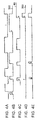
Fig. 1 is a block diagram showing the configuration of an optical disk apparatus according to an embodiment of the present invention; -
Fig. 2 is a detailed block diagram showing the photo-detector circuit shown inFig. 1 ; -
Fig. 3 is a block diagram showing a built-in sampling-timing-signal generating circuit in the photo-detector circuit shown inFig. 1 ; -
Fig. 4 is a timing chart illustrating the operation of the sampling-timing-signal generating circuit shown inFig. 3 ; -
Figs. 5A and 5B are graphs showing changes in the waveform of a signal when it passes through a flexible cable of the related art; and -
Fig. 6 is a schematic illustration of the positional relationship between a main spot and side spot in a differential push-pull method of the related art. -
Fig. 1 is a block diagram showing an optical disk apparatus according to an embodiment of the present invention. The optical disk apparatus includes an objective lens 1, a beam splitter (BS) 2, converging lenses 3 and 4, a semiconductor laser (LD) 5, a laser driving circuit (LDD) for driving thesemiconductor laser 5, a photo-detector circuit (PDIC) 7, a front-monitor photo-detector circuit (FPDIC) 8, an RFsignal processing circuit 9, a digital signal processor (DSP) 10, and acontroller 11. - The photo-detector circuit 7 includes a photo-detector (PD) 71, a current-voltage converter (I/V) 72, and sample-and-hold circuits (S/H) 73 and 74. The front-monitor detector circuit 8 includes a photo-detector (PD) 81, and a current-voltage converter (I/V) 82, and sample-and-hold circuits (S/H) 83 and 84. The RF
signal processing circuit 9 includes an optical photo coupler (OPC) 91, a wobble address detecting circuit (indicated by "WOBBLE ADDRESS") 92, a servo-signal generating circuit (indicated by "SERVO") 93, an RF signal generating circuit (indicated by "RF") 94, and an automatic emitting-power control circuit (APC) 95. Thedigital signal processor 10 includes aservo circuit 101, asignal processing circuit 102, adecoder 103, a write-strategy timing-generatingcircuit 104, and anencoder 105. The RFsignal processing circuit 9 corresponds to a signal processing means in the appended claims. -
Fig. 2 is a detailed block diagram showing the photo-detector circuit 7 shown inFig. 1 . As shown inFig. 6 , the photo-detector 71 has photo-receiving areas A to H for receiving portions of a main spot M and side spots S1 and S2. Signals which are obtained such that reflected beams are converted into corresponding currents in the photo-receiving areas A to H are converted into voltage signals by current-voltage conversion units. InFig. 2 , for brevity of description, typical current-voltage conversion units hold circuits 73D, 74D, and 74G. Actually, there are circuits corresponding to the photo-receiving areas. Accordingly, the number of configurations as shown inFig. 2 is four for the main spot, and the number of configurations as shown inFig. 2 is four for the side spots. Therefore, there are eight current-voltage converters 72A to 72H, four sample-and-hold circuits 73A to 73D, and eight sample-and-hold circuits 74A to 74H. The photo-receiving areas A to H of the photo-detector 71, and the current-voltage converters 72A, 72B, 72C, and 72D (only this is shown inFig. 2 ) correspond to a first converting means in the appended claims. The sample-and-hold circuits 74A, 74B, 74C, and 74D (only this is shown inFig. 2 ) correspond to a first sample-and-hold means in the appended claims. The areas E, F, G, and H of the photo-detector 71, and the current-voltage converters 72E, 72F, 72G (only this is shown inFig. 2 ), and 72H correspond to a second converting means in the appended claims. The sample-and-hold circuits 74E, 74F, 74G (only this is shown inFig. 2 ), and 74H correspond to a second sample-and-hold means in the appended claims. The main spot M shown inFig. 6 corresponds to a first spot in the appended claims. The side spots S1 and S2 shown inFig. 6 correspond to at least one second spot in the appended claims. - In the following description, the shown typical current-voltage converters and sample-and-hold circuits are used.
- Next, an operation of writing data to a disk in this embodiment is described below.
- The
controller 11 outputs writedata 200 to theencoder 105. Theencoder 105 encodes thewrite data 200 and outputs encodedwrite data 201 to the write-strategy timing-generatingcircuit 104. The write-strategy timing-generatingcircuit 104 generates write pulses in response to thewrite data 201, and outputs the generated write pulses to thelaser driving circuit 6. - The
laser driving circuit 6 performs power control in response to the write pulses by using bias power output. The modulated laser beam is converged on an optical disk 100 through the beam splitter 2 and the objective lens 1. In the writing process, a laser beam reflected by the optical disk 100 is split into two by the beam splitter 2. One split beam is input to the photo-detector 71 in the photo-detector circuit 7, and the other one slit beam is input to the photo-detector 81 in the front-monitor photo-detector circuit 8. - The photo-
detector 71 in the photo-detector circuit 7 receives and converts the beam into a corresponding current. The current-voltage converter 72 converts the current into a voltage and outputs the voltage as photo-reception signals to the sample-and-hold circuits 73 and 74. The sample-and-hold circuits 73 and 74 sample and hold the photo-reception signals and transmit the photo-reception signals to the RFsignal processing circuit 9 through a flexible cable (not shown). - Similarly, the photo-
detector 81 in the front-monitor photo-detector circuit 8 converts the beam into a corresponding current. The current-voltage converter 82 converts the current into a voltage and outputs the voltage as power monitor signals to the sample-and-hold circuits hold circuits signal processing circuit 9 through a flexible cable (not shown). - The operation of each sample-and-hold circuit used in the photo-detector circuit 7 is described below with reference to
Fig. 2 . - As shown in
Fig. 2 , the photo-detector circuit 7 has two circuit systems, that is, a main spot circuit system and a side spot circuit system. Compared with the sample-and-hold circuits 73D and 74D for the sample-and-hold circuits 73D and 74D for the main spot, the sample-and-hold circuit 74G for the side spot has a narrower bandwidth and its settling characteristic is designed to be longer. - Accordingly, in this embodiment, based on a sampling-
timing signal 302 for the main spot which is generated by the write-strategy timing-generatingcircuit 104, the photo-detector circuit 7 generates a sampling-timing signal for operating the sample-and-hold circuit 74G for the side spot. -
Fig. 3 is a block diagram showing a circuit that generates a sampling-timing signal 350 for the side spot circuit system based on the sampling-timing signal 302. A sample-timing generating circuit 60 includes adelay circuit 30, an SR flip-flop 31, and D flip-flops flop 31 can respectively act to perform setting and resetting operations at rise edges. The resetting terminals (R) of the D flip-flops - The sampling-
timing signal 302 shown inFig. 4B is originally used for sampling and holding in the main spot circuit system. Thus, it is directly input to a sample-and-hold circuit in the main spot circuit system. In other words, the sampling-timing signal 302 is directly input to the sample-and-hold circuit 74D in the main spot circuit system. The sample-and-hold circuit 74D samples low-level-period portions of the photoelectrically converted signal (corresponding to write data) in high level periods of the sampling-timing signal 302, which is input to the sample-and-hold circuit 74D. The sample-and-hold circuit 73D in the main spot circuit system operates based on the sampling-timing signal 301. - In the case of generating the sampling-
timing signal 350 shown inFig. 4D by the sample-and-hold circuit 74G based on the sampling-timing signal 302, by generating the sampling-timing signal 350 when the sampling-timing signal 302 has the long period indicated by reference letter a shown inFig. 4B , the generated sampling-timing signal 350 has a narrow bandwidth and a long settling characteristic, and is adapted for the current-voltage converter 72G in the side spot circuit system. - The sampling-
timing signal 302 is input to the sample-and-hold circuit 74D and is also input to thedelay circuit 30, so that the delayedsignal 80 shown inFig. 4C is generated and is input to the resetting terminal (R) of the SR flip-flop 31. The sampling-timing signal 302 is input to the setting terminal (S) of the SR flip-flop 31. The output of the inverted output terminal (xQ) of the SR flip-flop 31 is input to a data terminal (D) of the D flip-flop 32, and the sampling-timing signal 302 is input to a clock terminal (ck) and resetting terminal (R) of the D flip-flop 32. The clock terminal (ck) acts to operate at a rise edge. The resetting terminal (R) acts to operate at a fall edge. The output of the output terminal (Q) of the D flip-flop 32 is input to a data terminal (D) of the D flip-flop 33. The delayedsignal 80 is input to the D flip-flop 33. The sampling-timing signal 302 is input to the resetting terminal (R) of the D flip-flop 33. The clock terminal (ck) of the D flip-flop 33 also acts to operate at a fall edge, and the resetting terminal (R) of the D flip-flop 33 acts to operate at a fall edge. - In a state in which the SR flip-
flop 31 is reset when the sampling-timing signal 302 is at low level and the delayedsignal 80 is also at low level, the inverted output (xQ) of the SR flip-flop 31 is at high level. This allows the D flip-flop 32 to be operable since a high level signal is input to the data terminal (D) of the D flip-flop 32, so that the output of the output terminal (Q) is at low level. - At this time, at an edge at which the sampling-
timing signal 302 is at high level as denoted by reference letter a shown inFig. 4B , the D flip-flop 32 operates, and its output terminal (Q) becomes high in level, and the SR flip-flop 31 is set, so that the output of the inverted output terminal (xQ) becomes low in level. When the output terminal (Q) of the D flip-flop 32 becomes high in level, the data terminal (D) of the D flip-flop 33 becomes high in level. This allows the D flip-flop 33 to be operable. However, the output (similar to the sampling-timing signal 350) of the output terminal (Q) of the D flip-flop 33 is still at low level. - Before the sampling-
timing signal 302 rises in this state, when the delayedsignal 80 changes to be in high level, as denoted by reference letter b, the D flip-flop 33 operates and its output Q becomes high in level, so that the sampling-timing signal 350 rises as denoted by reference letter c. Then, the delayedsignal 80 resets the SR flip-flop 31, and the output of the inverted output terminal xQ becomes high in level. In this state, when the sampling-timing signal 302 rises in low level, the D flip-flops flop 33 becomes low in level, thus causing the sampling-timing signal 350 to fall. After all, the sampling-timing signal 350 is output with it delayed for the sampling-timing signal 302. - However, although the sampling-
timing signal 302 falls as denoted by reference letter d inFig. 4B , when the sampling-timing signal 302 falls before the delayedsignal 80 changes to be in high level, the D flip-flop 33 is reset and its output terminal Q has a low level output. In this state, even if the delayedsignal 80 rises as denoted by reference letter e inFig. 4C , the D flip-flop 33 does not operate and its output terminal Q remains to have a low level output, so that the sampling-timing signal 350 is not output as denoted by reference letter f inFig. 4D . Therefore, by preventing the sampling-timing signal 302 from being mistakenly output as denoted by reference letters g and h when the sampling-timing signal 302 is short, the sampling-timing signal 350, which is suitable for the sampling and holding operation of the sample-and-hold circuit 74G for the side spot circuit system, is generated. - Therefore, it may be said that the sampling-
timing generating circuit 60 shown inFig. 3 is a circuit in which, after the sampling-timing signal 302 rises, before the sampling-timing signal 302 falls, only when the delayedsignal 80 rises does the circuit output the sampling-timing signal 350. - When the photoelectrically converted signal shown in
Fig. 4A , which is input, has long bias periods (low level periods) as denoted by reference letter i, the sample-and-hold circuit 74G in the side spot circuit system samples and holds the above photoelectrically converted signal in the bias periods based on the sampling-timing signal 350 shown inFig. 4D . In addition, the sample-and-hold circuit 74D performs a sampling and holding operation based on the sampling-timing signal 302. The sample-and-hold circuit 74D does not use a sampling-timing signal separately generated as described above. - The sample-and-
hold circuits hold circuits hold circuits signals - A signal held by the sample-and-hold circuit 73 in the photo-detector circuit 7 is transmitted to the optical photo coupler (OPC) 91 and the wobble
address detecting circuit 92 in the RFsignal processing circuit 9 through the flexible cable. A signal held by theaddress counter 74 is transmitted to the wobbleaddress detecting circuit 92, the servo-signal generating circuit 93, and the RFsignal generating circuit 94, and the frequency characteristics and level of the read signal are shaped to generate an RF signal. - A signal held by the sample-and-
hold circuit 83 in the front-monitor photo-detector circuit 8 is transmitted to theAPC 95 in the RFsignal processing circuit 9, and a signal held by theadaptive filter 84 is also transmitted to theAPC 95 through the flexible cable. - The optical photo coupler (OPC) 91 in the RF
signal processing circuit 9 finds an optical recording output level of thesemiconductor laser 5 based on the level of the photo-reception signal in the recording period, and sets the optical recording output level in theAPC 95. TheAPC 95 performs control in which, based on the level of a power monitor signal in the recording and bias periods, the emission power of thesemiconductor laser 5 is used as a set value. - The servo-
signal generating circuit 93 calculates, based on a sampling signal of the photo-reception signal in the bias period, various servo signals, and outputs the calculated signals to theservo circuit 101 in thedigital signal processor 10. Theservo circuit 101 generates, based on the input servo signals, a servo signal for driving an actuator (not shown), and outputs the servo signal to the actuator. This performs tracking control and focusing control of the optical pickup including the photo-detector circuit 7, the front-monitor photo-detector circuit 8, and the optical system (thesemiconductor laser 5, the beam splitter 2, the objective lens 1, etc.). - Based on the sampling signals of the photo-reception signals in the recording period and the bias period, the wobble
address detecting circuit 92 detects an absolute address. Based on the address, thecontroller 11 constantly monitors a position on the optical disk 100 at which data is currently recorded. When no data is recorded at a predetermined position, theservo circuit 101 is controlled to perform an operation such as re-recording. In addition, thecontroller 11 performs on-off control of theencoder 105, thespindle motor 103, and theservo circuit 101, and controls the apparatus entirety. Specifically, thecontroller 11 controls the entirety to reflect user's instructions input through an interface such as an operation panel (not shown), and to display an apparatus status on a display of the operation panel. - When the optical disk 100 is played back, the sampled-and-held signals are input from the sample-and-
hold circuit 74 in the photo-detector circuit 7 and the sample-and-hold circuit 84 in the front-monitor photo-detector circuit 8 to the RFsignal generating circuit 94. The RFsignal generating circuit 94 in the RFsignal processing circuit 9 processes the input sample-and-hold circuit into an RF signal by equalizing the frequency of the input sampled-and-held signal and shaping the level of the input sampled-and-held signal, and outputs the RF signal to thesignal processing circuit 102 in thedigital signal processor 10. Thesignal processing circuit 102 binarizes the RF signal into a read data and outputs the read data to thedecoder 103. Thedecoder 103 decodes the read data into user data and outputs the user data to thecontroller 11. The operations of the servo-signal generating circuit 93 and theservo circuit 101 are similar to those in the recording time. In addition, theAPC 95 controls, based on the sampled-and-held signal input from the sample-and-hold circuit 84, the semiconductor-laser emission power at a predetermined constant level. - In this embodiment, the sampling-timing
signals digital signal processor 10 to the photo-detector circuit 7 through the flexible cable. However, by using the sampling-timing signal 350 generated by the sampling-timing generating circuit 60 in the photo-detector circuit 7 based on the sampling-timing signal 302, the sample-and-hold circuit 74G for the side spot is operated. Therefore, it is not necessary for thedigital signal processor 10 to transmit, to the photo-detector circuit 7, a dedicated sampling-timing signal for operating the sample-and-hold circuit 74G for the side spot. Accordingly, by reducing the number of wires in the flexible cable, the size of the flexible cable can be prevented from being increased. This contributes to a reduction in apparatus size. - Based on the sampling-
timing signal 302 and the delayedsignal 80 of the sampling-timing signal 302, the sampling-timing signal 350 is generated. In this generating process, after the sampling-timing signal 302 rises, before the sampling-timing signal 302 falls, only when the delayedsignal 80 rises does the sampling-timing generating circuit 60 output the sampling-timing signal 350. This can generate the sampling-timing signal 350, which is free from a pseudo-component and is accurate. - In addition, since the sample-and-
hold circuit 74G for the side spot is operated based on the sampling-timing signal 350, which is dedicated therefor, a circuit for the side spot is set to have a narrow bandwidth and long settling. This can reduce circuit size and cost. - Moreover, the photo-detector circuit 7 and the front-monitor photo-detector circuit 8 sample photo-reception signals and power-monitor signals and send sampled-and-held signals to the RF
signal processing circuit 9 at the subsequent stage through the flexible cable. Therefore, in each of the photo-detector circuit 7 and the front-monitor photo-detector circuit 8, in the settling time from the recording power level at sampling to the bias power level, it is not necessary to drive the flexible cable. Thus, the slew rate of the initial stage can be sufficiently shortened, thus enabling accurate sampling even if recording speed is increased, so that a stable and accurate sampled-and-held signal can be transmitted to the RFsignal processing circuit 9. This enables various types of signal processing in the RFsignal processing circuit 9 to be accurately and stably performed. Accordingly, even at large recording speed, smooth data recording can be performed. - While the present invention has been described with reference to what are presently considered to be the preferred embodiments, it is to be understood that the invention is not limited to the disclosed embodiments. On the contrary, the invention includes various modifications and equivalent arrangements included coming within the scope of the appended claims.
Claims (5)
- An optical disk apparatus for obtaining a plurality of servo signals by separating a laser beam into at least two beams, converging said at least two beams on a main spot (M) as a first spot and at least one side spot (S1, S2) as second spot on a recording medium (100), and photoelectrically converting reflected beams from the first spot (M) and said at least one second spot (S1, S2) at the time of recording data on the recording medium (100), the optical disk apparatus comprising:first converting means (A-D, 72A-D) for converting the reflected beam from the first spot (M) into an electrical signal;first sample-and-hold means (74A-D) for sampling and holding the electrical signal obtained by the first converting means (A-D, 72A-D);second converting means (E-H, 72E-H) for converting the reflected beam from said at least one second spot (S1, S2) into an electrical signal;second sample-and-hold means (74E-H) for sampling and holding the electrical signal obtained by the second converting means (E-H, 72E-H);signal generating means (60) for generating, based on a given first sampling-timing signal (302) for determining sampling timing for the first sample-and-hold means (74A-D), a second sampling-timing signal (350) for determining sampling timing for the second sample-and-hold means (74E-H); anda flexible cable as a transmitting means for transmitting, to signal processing circuits (91-95) at a subsequent stage (9), sampled-and-held signals obtained by the first and second sample-and-hold means (74A-D; 74E-H),wherein said first and second converting means (A-D, 72A-D; E-H, 72E-H), said first and second sample-and-hold means (74A-D; 74E-H) and said signal generating means are integrated into a single integrated chip circuit (7, PDIC).
- The optical disk apparatus according to claim 1, wherein, based on the generated second sampling-timing signal (350), the second sample-and-hold means (74E-H) samples and holds the electrical signal obtained by the second converting means (E-H, 72E-H) in a period in which the laser beam is emitted at a bias power level.
- The optical disk apparatus according to claim 1, wherein, the signal generating means (60) generates the second sampling-timing signal (350) based on the first sampling-timing signal (302) and a delayed signal (80) obtained by delaying the first sampling-timing signal (302).
- The optical disk apparatus according to claim 3, wherein, before the first sampling-timing signal (302) falls, the signal generating means (60) generates the second sampling-timing signal (350) only when the delayed signal (80) rises.
- The optical disk apparatus according to claim 1, wherein each of the side spots (S1, S2) is radially disposed on the recording medium (100) in a form shifted with respect to the main spot (M) by half of a track pitch (P).
Applications Claiming Priority (2)
| Application Number | Priority Date | Filing Date | Title |
|---|---|---|---|
| JP2003371535A JP3879928B2 (en) | 2003-10-31 | 2003-10-31 | Optical disk device |
| JP2003371535 | 2003-10-31 |
Publications (3)
| Publication Number | Publication Date |
|---|---|
| EP1528543A2 EP1528543A2 (en) | 2005-05-04 |
| EP1528543A3 EP1528543A3 (en) | 2007-04-04 |
| EP1528543B1 true EP1528543B1 (en) | 2009-03-04 |
Family
ID=34420227
Family Applications (1)
| Application Number | Title | Priority Date | Filing Date |
|---|---|---|---|
| EP04024986A Expired - Fee Related EP1528543B1 (en) | 2003-10-31 | 2004-10-20 | Optical disk apparatus |
Country Status (5)
| Country | Link |
|---|---|
| EP (1) | EP1528543B1 (en) |
| JP (1) | JP3879928B2 (en) |
| KR (1) | KR20050041883A (en) |
| DE (1) | DE602004019743D1 (en) |
| TW (1) | TWI255445B (en) |
Families Citing this family (1)
| Publication number | Priority date | Publication date | Assignee | Title |
|---|---|---|---|---|
| TW200809831A (en) * | 2006-06-26 | 2008-02-16 | Koninkl Philips Electronics Nv | Disc drive and photo-detector circuits |
Family Cites Families (2)
| Publication number | Priority date | Publication date | Assignee | Title |
|---|---|---|---|---|
| JP2001357544A (en) | 2000-06-16 | 2001-12-26 | Ricoh Co Ltd | Optical disk device |
| JP3828415B2 (en) | 2001-12-10 | 2006-10-04 | 株式会社東芝 | Optical disc device and optical head device |
-
2003
- 2003-10-31 JP JP2003371535A patent/JP3879928B2/en not_active Expired - Fee Related
-
2004
- 2004-10-15 KR KR1020040082546A patent/KR20050041883A/en active IP Right Grant
- 2004-10-20 DE DE602004019743T patent/DE602004019743D1/en not_active Expired - Fee Related
- 2004-10-20 EP EP04024986A patent/EP1528543B1/en not_active Expired - Fee Related
- 2004-10-29 TW TW093133069A patent/TWI255445B/en not_active IP Right Cessation
Also Published As
| Publication number | Publication date |
|---|---|
| DE602004019743D1 (en) | 2009-04-16 |
| TW200519849A (en) | 2005-06-16 |
| JP2005135534A (en) | 2005-05-26 |
| EP1528543A2 (en) | 2005-05-04 |
| EP1528543A3 (en) | 2007-04-04 |
| JP3879928B2 (en) | 2007-02-14 |
| KR20050041883A (en) | 2005-05-04 |
| TWI255445B (en) | 2006-05-21 |
Similar Documents
| Publication | Publication Date | Title |
|---|---|---|
| US7307930B2 (en) | Optical disk apparatus | |
| USRE43105E1 (en) | Tracking error detection method and optical disc reproduction apparatus using the same | |
| EP1528543B1 (en) | Optical disk apparatus | |
| JP4492810B2 (en) | Attenuation adjustment circuit, optical disc drive apparatus, attenuation adjustment method, and address information acquisition method | |
| US8193958B2 (en) | Signal regenerator | |
| JP4019280B2 (en) | Optical disk device | |
| US7068571B2 (en) | Optical recording apparatus and control method thereof | |
| JPH09161285A (en) | Tracking error detecting device | |
| US20060114766A1 (en) | Wobbling signal reproduction device | |
| JP3604125B2 (en) | Optical pickup device | |
| CN101206883B (en) | Optical pickup apparatus | |
| JP2008176882A (en) | Front monitor device, optical pickup device provided with the same, and information recording and reproducing device | |
| JP3240462B2 (en) | Optical pickup servo device for optical disk drive | |
| KR100432847B1 (en) | An apparatus and method for detecting wobble signal | |
| JP2005032373A (en) | Photodetector device, optical pickup device, optical recording device, and integrated circuit | |
| KR100243871B1 (en) | Device and method of discriminating cd/dvd disk | |
| JP2003228867A (en) | Optical pickup device and optical disk drive | |
| JPH1139688A (en) | Photodetector and optical pickup device | |
| JP2005032341A (en) | Optical disk device | |
| KR20030016803A (en) | Optical pick-up | |
| JP2002042363A (en) | Optical disk device | |
| JP2000030267A (en) | Track jump detection circuit of disk player | |
| WO2008141126A2 (en) | Signal regenerator | |
| JP2005078751A (en) | Optical disk device and its laser power control method | |
| KR19980077500A (en) | CD / DVD combined pickup unit with collimator lens removed |
Legal Events
| Date | Code | Title | Description |
|---|---|---|---|
| PUAI | Public reference made under article 153(3) epc to a published international application that has entered the european phase |
Free format text: ORIGINAL CODE: 0009012 |
|
| AK | Designated contracting states |
Kind code of ref document: A2 Designated state(s): AT BE BG CH CY CZ DE DK EE ES FI FR GB GR HU IE IT LI LU MC NL PL PT RO SE SI SK TR |
|
| AX | Request for extension of the european patent |
Extension state: AL HR LT LV MK |
|
| RTI1 | Title (correction) |
Free format text: OPTICAL DISK APPARATUS |
|
| PUAL | Search report despatched |
Free format text: ORIGINAL CODE: 0009013 |
|
| AK | Designated contracting states |
Kind code of ref document: A3 Designated state(s): AT BE BG CH CY CZ DE DK EE ES FI FR GB GR HU IE IT LI LU MC NL PL PT RO SE SI SK TR |
|
| AX | Request for extension of the european patent |
Extension state: AL HR LT LV MK |
|
| RIC1 | Information provided on ipc code assigned before grant |
Ipc: G11B 7/0045 20060101ALI20070227BHEP Ipc: G11B 7/09 20060101AFI20070227BHEP Ipc: G11B 7/12 20060101ALI20070227BHEP |
|
| 17P | Request for examination filed |
Effective date: 20070912 |
|
| AKX | Designation fees paid |
Designated state(s): DE FR GB |
|
| 17Q | First examination report despatched |
Effective date: 20071214 |
|
| GRAP | Despatch of communication of intention to grant a patent |
Free format text: ORIGINAL CODE: EPIDOSNIGR1 |
|
| GRAS | Grant fee paid |
Free format text: ORIGINAL CODE: EPIDOSNIGR3 |
|
| GRAA | (expected) grant |
Free format text: ORIGINAL CODE: 0009210 |
|
| AK | Designated contracting states |
Kind code of ref document: B1 Designated state(s): DE FR GB |
|
| REG | Reference to a national code |
Ref country code: GB Ref legal event code: FG4D |
|
| REF | Corresponds to: |
Ref document number: 602004019743 Country of ref document: DE Date of ref document: 20090416 Kind code of ref document: P |
|
| PLBE | No opposition filed within time limit |
Free format text: ORIGINAL CODE: 0009261 |
|
| STAA | Information on the status of an ep patent application or granted ep patent |
Free format text: STATUS: NO OPPOSITION FILED WITHIN TIME LIMIT |
|
| 26N | No opposition filed |
Effective date: 20091207 |
|
| REG | Reference to a national code |
Ref country code: FR Ref legal event code: ST Effective date: 20100630 |
|
| PG25 | Lapsed in a contracting state [announced via postgrant information from national office to epo] |
Ref country code: DE Free format text: LAPSE BECAUSE OF NON-PAYMENT OF DUE FEES Effective date: 20100501 Ref country code: FR Free format text: LAPSE BECAUSE OF NON-PAYMENT OF DUE FEES Effective date: 20091102 |
|
| PG25 | Lapsed in a contracting state [announced via postgrant information from national office to epo] |
Ref country code: GB Free format text: LAPSE BECAUSE OF NON-PAYMENT OF DUE FEES Effective date: 20091020 |