EP1526602B1 - Drahtlose Netzwerkkarte mit verbesserter Antennenempfindlichkeit - Google Patents
Drahtlose Netzwerkkarte mit verbesserter Antennenempfindlichkeit Download PDFInfo
- Publication number
- EP1526602B1 EP1526602B1 EP04025171A EP04025171A EP1526602B1 EP 1526602 B1 EP1526602 B1 EP 1526602B1 EP 04025171 A EP04025171 A EP 04025171A EP 04025171 A EP04025171 A EP 04025171A EP 1526602 B1 EP1526602 B1 EP 1526602B1
- Authority
- EP
- European Patent Office
- Prior art keywords
- radiating
- wireless network
- conductor pattern
- network card
- board
- Prior art date
- Legal status (The legal status is an assumption and is not a legal conclusion. Google has not performed a legal analysis and makes no representation as to the accuracy of the status listed.)
- Expired - Lifetime
Links
Images

Classifications
-
- H—ELECTRICITY
- H01—ELECTRIC ELEMENTS
- H01Q—ANTENNAS, i.e. RADIO AERIALS
- H01Q1/00—Details of, or arrangements associated with, antennas
- H01Q1/12—Supports; Mounting means
- H01Q1/22—Supports; Mounting means by structural association with other equipment or articles
- H01Q1/2258—Supports; Mounting means by structural association with other equipment or articles used with computer equipment
- H01Q1/2275—Supports; Mounting means by structural association with other equipment or articles used with computer equipment associated to expansion card or bus, e.g. in PCMCIA, PC cards, Wireless USB
-
- H—ELECTRICITY
- H01—ELECTRIC ELEMENTS
- H01Q—ANTENNAS, i.e. RADIO AERIALS
- H01Q9/00—Electrically-short antennas having dimensions not more than twice the operating wavelength and consisting of conductive active radiating elements
- H01Q9/04—Resonant antennas
Definitions
- the present invention relates to a wireless network card according to the preamble of claim 1, such as a wireless LAN card, which is inserted into a main apparatus of a notebook computer or the like.
- a wireless network card of this type is known from US-A-6,559,809 .
- card slots for inserting PC cards such as wireless LAN cards
- the wireless LAN cards are installed in the notebook computers
- the wireless LAN cards having a transmitting and receiving function are inserted into the card slots so that the wireless LAN cards transmit and receive signals to and from CPUs of the notebook computers.
- antenna units, ground conductor patterns and electronic circuit units RF circuits and control circuits
- RF circuits and control circuits are arranged for transmitting and receiving radio waves that have a predetermined frequency bandwidth (for example, 2.4 GHz) for the wireless LANs.
- the PC cards having such antennas built therein are generally referred to as wireless network cards.
- antennas In conventional wireless network cards, pattern antennas, dielectric antennas or metal sheet antennas are widely used for antenna units.
- the use of erected rod antennas has also been suggested (for example, see Japanese Unexamined Patent Publication No. 9-167125 ; page 3, Fig. 1).
- the antenna unit is usually provided on one side of a card-shaped board.
- the ground conductor pattern operating serving as a ground of the antenna unit and the electronic circuit unit for supplying power to the antenna unit are provided on the board such that it occupies a relatively broad space of the board surface.
- a radiating element is a monopole-type radiating conductor pattern
- a feeding line On one surface of a card-shaped board an electronic circuit unit, a feeding line, and a radiating conductor pattern are provided.
- a separate electronic circuit unit and a ground conductor pattern On the other surface of the board, often, a separate electronic circuit unit and a ground conductor pattern are provided.
- the ground conductor pattern is provided over a broad region, except for the side of the board where the radiating conductor pattern is provided.
- the feeding line is a micro-strip line, and one end of the feeding line is connected to the electronic circuit unit and the other end of the feeding line is connected to the radiating conductor pattern.
- the feeding line faces the ground conductor pattern via the board.
- the antenna unit is a pattern antenna, it is suitable for making the wireless network card to be smaller in thickness and to lower the manufacturing cost.
- the antenna unit in a state where the wireless network card is inserted in a notebook computer, the antenna unit is provided on one side of the board that protrudes to the outside of the main apparatus such as the notebook computer, and electrical waves are externally radiated from the antenna unit.
- the ground conductor pattern that is inserted into the main apparatus such as the notebook computer is larger than the radiating element of the antenna unit.
- the radiating element when excited, an induced current is easily generated in the ground conductor pattern in the vicinity of the radiating element. As a result, there is a problem in that radiation beams are often attracted to the ground conductor pattern side.
- the directivity is stronger in a desired direction away from the main apparatus.
- the radio waves radiated to the side of the main apparatus suddenly become stronger.
- the directivity of the radio waves becomes weak in the desired direction, and consequently the sensitivity of the antenna decreases. Further, an erroneous operation of the main apparatus may also occur.
- the present invention has been made to solve the above-mentioned problems, and it is an object of the present invention to provide a wireless network card in which the directivity of an radio wave in a desired direction away from a main apparatus is stronger than other directions with an improved sensitivity.
- the present invention provides a wireless network card which comprises the features of claim 1.
- the wireless network card having such structure, even though the radiating element (conductor pattern) is excited and an induced current is then generated in the ground conductor pattern in the vicinity of the radiating element, most of the induced current is eliminated when the induced current reaches the choking slit. Therefore, the induced current that flows into the ground conductor pattern can be drastically suppressed.
- the directivity of the radio wave radiated from the radiating element does not lean toward the ground conductor pattern side because of the influence of the induced current, the directivity of the radio wave is strong in a predetermined direction away from the main apparatus, and the strong beams is radiated toward the main apparatus into which the ground conductor pattern is inserted. As a result, an erroneous operation of the main apparatus is not caused.
- a preferred embodiment is defined by the dependent claim.
- the induced current generated in the ground conductor pattern in the vicinity of the radiating element particularly flows along the circumferential edge of the ground conductor pattern. Therefore, if the cutout having a depth of about ⁇ /4 is provided in the circumferential edge of the ground conductor pattern located on the region that is relatively close to the radiating element, the induced current that flows to a side opposite to the side of the radiating element can be effectively suppressed by a choking function of the cutout.
- an elongated hole is formed in the ground conductor pattern to form the choking slit, and the choking slit is set such that its length is 1/2 of a resonant wavelength ⁇ of a tuning radio wave in which the radiating element resonates.
- the induced current that flows through the ground conductor pattern which is a side opposite to the side of the radiating element can be effectively suppressed by a choking function of the elongated hole having a length of about ⁇ /2.
- the wireless network card having the above-mentioned structure, when the radiating element is a monopole-type radiating conductor pattern which is provided on the one surface of the board having the feeding line, a pattern antenna having a simple structure and an improved sensitivity can be obtained. Therefore, it is suitable for making the wireless network card to be smaller in thickness and to lower the manufacturing cost.
- the wireless network card further comprises a pair of the radiating conductor patterns substantially orthogonal to each other in their extending directions; and a pair of the feeding lines connected to the pair of radiating conductor patterns, respectively.
- a multipass does not affect the diversity antenna. It can be operated as a diversity antenna having a high reliability. Therefore, the practical value thereof becomes high.
- Fig. 1 is a plan view of a wireless network card according to a first embodiment of the present invention
- Fig. 2 is an explanatory view illustrating a state where the wireless network card is inserted into a notebook computer
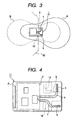
- Fig. 3 is an explanatory view illustrating a directional characteristic of radiation beams of the wireless network card.
- a wireless network card 1 comprises a card-shaped board 2 on which an electronic circuit unit 3 is arranged; a pair of radiating conductor patterns 4 and 5 that are pattern antennas provided on one side of one surface of the board 2 and that are substantially orthogonal to each other in their extending directions; a pair of feeding lines 6 and 7 that are micro-strip lines provided on one surface of the board 2, one end of each of feeding lines being connected to the electronic circuit unit 3; and a ground conductor pattern 8 serving as a ground of the radiating conductor patterns 4 and 5 and that is provided on the other surface of the board 2.
- the electronic circuit unit 3 comprises a diversity receiving circuit or a RF circuit or a control circuit.
- Each of the radiating conductor patterns 4 and 5 is a monopole-type radiating conductor pattern that the length thereof is set to about 1/4 of the resonant length (the wavelength of a tuning radio wave in which the radiating conductor patterns 4 and 5 resonate) ⁇ .
- One end of the feeding line 6 is connected to the electronic circuit unit 3 and the other end of the feeding line 6 is connected to the radiating conductor pattern 4.
- one end of the feeding line 7 is connected to the electronic circuit unit 3 and the other end of the feeding line 7 is connected to the radiating conductor pattern 5.
- the ground conductor pattern 8 is formed over a relatively broad region on the board 2. However, in the ground conductor pattern 8, a pattern shape is designed so as not to face the monopole-type radiating conductor patterns 4 and 5.
- a pair of choking slits 9 and 10 is formed in a region of the ground conductor pattern 8 that does not overlap the feeding lines 6 and 7 between the electronic circuit unit 3 and the radiating conductor patterns 4 and 5.
- the pair of choking slits 9 and 10 is set to the length that makes it difficult for a high-frequency current to flow through the electronic circuit unit'.
- a pair of concave cutouts is provided at a circumferential edge of the ground conductor pattern 8 relatively close to the radiating conductor patterns 4 and 5, thereby forming the choking slits 9 and 10.
- Each of the choking slits 9 and 10 is set such that the length (depth) thereof is about 1/4 of the resonant length ⁇ .
- the choking slits 9 and 10 are formed in a region that does not face the feeding lines 6 and 7 via a board 2.
- the choking slits 9 and 10 prevents an induced current generated in the ground conductor pattern 8 in the vicinity of the radiating conductor patterns 4 and 5 from flowing into the electronic circuit unit 3.
- the wireless network card 1 having the above-mentioned structure is inserted into a slot 21 for card of a notebook computer 20 and is then used.
- the wireless network card is configured such that a radio wave is externally radiated from the radiation conductor patterns 4 and 5, which are not inserted into the notebook computer 20.
- the radiating conductor patterns 4 and 5 are supplied with power from the feeding lines 6 and 7, respectively, to be excited.
- the signals received by the respective radiating conductor patterns 4 and 5 are transmitted to the diversity receiving circuit of the electronic circuit unit 3. Then, by the diversity receiving circuit of the electronic circuit unit 3, the signals having a large receiving power are selected or both signals are synthesized.
- the ground conductor pattern 8 that is inserted into the notebook computer 20 is larger than the radiating conductor patterns 4 and 5, when the radiating conductor patterns 4 and 5 are excited, an induced current is easily generated in the ground conductor pattern 8 in the vicinity of the radiating conductor patterns 4 and 5.
- the choking slits (cutouts) 9 and 10 having a depth of about ⁇ /4 are provided at a circumferential edge of the ground conductor pattern 8 in a region that is relatively close to the radiating conductor patterns 4 and 5.
- the radiating conductor patterns 4 and 5 are excited, when the induced current that flows to a side opposite to the side of the radiating conductor patterns 4 and 5 reaches the choking slits 9 and 10, most of the induced current is eliminated. Thus, the induced current that flows into the ground conductor pattern 8 can be drastically suppressed. As a result, a directional characteristic of radiation beams of the wireless network card 1 forms a curved line A denoted by a solid line in Fig. 3. Further, the radio wave is strongly radiated to the side away from the notebook computer 20.
- a curved line B denoted by a broken line in Fig. 3 is a comparative example illustrating a directional characteristic in the case where the choking slits 9 and 10 is not provided in the ground conductor pattern 8.
- Fig. 4 is a plan view of a wireless network card according a second embodiment of the present invention.
- the same elements as those in Fig. 1 are indicated by the same reference numerals.
- a wireless network card 11 according to the second embodiment is different from the wireless network card 1 according the first embodiment, in that an elongated hole is formed in a ground conductor pattern 8 to form a choking slit 12.
- the choking slit 12 is set such that its length is 1/2 of a resonant length ⁇ . Specifically, when radiating conductor patterns are excited, an induced current generated in the ground conductor pattern 8 flows not only to a circumferential edge of the ground conductor pattern 8 but also to the inside of the ground conductor pattern 8.
- the choking slit 12 is provided inside the ground conductor pattern 8 that is relatively close to the radiating conductor patterns 4 and 5. Since the slit 12 has an elongated hole shape with its both ends closed, the length of the slit 12 is set to about ⁇ /2, and thus a choke effect can be obtained. However, similarly to the choking slits 9 and 10, the choking slit 12 is formed at a proper position that does not overlap feeding lines 6 and 7.
- the antenna units provided on one side of the board 2 are pattern antennas (the radiating conductor patterns 4 and 5), it is suitable for making the wireless network card to be smaller in thickness and to lower the manufacturing cost. Furthermore, since the pair of radiating conductor patterns 4 and 5, the pair of feeding lines 6 and 7, and the diversity receiving circuit constitutes a diversity antenna, a multipass does not affect the diversity antenna, thereby obtaining a high reliability and increasing a practical value.
- the antenna unit is made of a dielectric antenna or a metal sheet antenna, or even when the antenna unit does not adopt a diversity type, if the choking slits having a predetermined length (the cutouts or the elongated hole) are provided in the ground conductor pattern in a region that is relatively close to the radiating elements, the same effect can be expected.
- the choking slits are provided in the ground conductor pattern.
- the directivity of the radio wave radiated from the radiating elements does not lean toward the ground conductor pattern side caused by the influence of the induced current. Therefore, the directivity of the radio wave in a predetermined direction becomes stronger than other directions and the sensitivity of the antenna can be increased. Also, since strong beams are not radiated toward the main apparatus, such as the notebook computer, into which the ground conductor pattern is inserted, the erroneous operation of the main apparatus does not occur.
Landscapes
- Engineering & Computer Science (AREA)
- Computer Networks & Wireless Communication (AREA)
- Computer Hardware Design (AREA)
- General Engineering & Computer Science (AREA)
- Support Of Aerials (AREA)
- Waveguide Aerials (AREA)
- Details Of Aerials (AREA)
- Transceivers (AREA)
- Variable-Direction Aerials And Aerial Arrays (AREA)
Claims (2)
- Drahtlose Netzwerkkarte, aufweisend:eine Platine (2), auf der eine elektronische Schaltungseinheit (3) angeordnet ist;Strahlungselemente mit Strahlungsleiterstrukturen (4, 5), die auf einer Seite der Platine vorgesehen sind;eine Speiseleitung (6, 7), die an der einen Oberfläche der Platine vorgesehen ist, wobei das eine Ende der Speiseleitung mit der elektronischen Schaltungseinheit (3) verbunden ist und das andere Ende der Speiseleitung (6, 7) mit den Strahlungselementen verbunden ist, und eine Erdungsleiterstruktur (8), die als Erdung der Strahlungsleiterstrukturen dient und auf der anderen Oberfläche der Platine (2) derart vorgesehen ist, dass sie zumindest der Speiseleitung (6, 7) über die Platine (2) hinweg gegenüberliegt,wobei ein länglicher Ausschnitt (9, 10; 12) in einem Bereich der Erdungsleiterstruktur (8), der die Speiseleitung (6, 7) nicht überlappt, zwischen der elektronischen Schaltungseinheit (3) und den Strahlungsleiterstrukturen (4, 5) gebildet ist, um einen Drosselschlitz zu bilden, und wobei der Drosselschlitz derart vorgegeben ist, dass seine Länge ca. 1 /2 einer Wellenlänge ë einer Abstimmfunkwelle beträgt, mit der die Strahlungselemente schwingen,dadurch gekennzeichnet, dass der Ausschnitt einen Schlitz zwischen der elektronischen Schaltung und jeder der beiden Strahlungsleiterstrukturen (4, 5) vom Monopol-Typ aufweist, die auf der einen Oberfläche der Platine, die die Speiseleitung (6, 7) aufweist, vorgesehen sind.
- Drahtlose Netzwerkkarte nach Anspruch 1,
weiterhin aufweisend:ein Paar der Strahlungsleiterstrukturen (4, 5), die in ihren Erstreckungsrichtungen im Wesentlichen orthogonal zueinander sind; undein Paar der Speiseleitungen (6, 7), das mit dem Paar der Strahlungsleiterstrukturen verbunden ist,wobei eine Diversity-Empfangsschaltung in der elektronischen Schaltungseinheit (3) vorgesehen ist.
Applications Claiming Priority (2)
| Application Number | Priority Date | Filing Date | Title |
|---|---|---|---|
| JP2003363502 | 2003-10-23 | ||
| JP2003363502A JP2005130188A (ja) | 2003-10-23 | 2003-10-23 | 無線ネットワークカード |
Publications (2)
| Publication Number | Publication Date |
|---|---|
| EP1526602A1 EP1526602A1 (de) | 2005-04-27 |
| EP1526602B1 true EP1526602B1 (de) | 2007-12-12 |
Family
ID=34386528
Family Applications (1)
| Application Number | Title | Priority Date | Filing Date |
|---|---|---|---|
| EP04025171A Expired - Lifetime EP1526602B1 (de) | 2003-10-23 | 2004-10-22 | Drahtlose Netzwerkkarte mit verbesserter Antennenempfindlichkeit |
Country Status (4)
| Country | Link |
|---|---|
| US (1) | US20050090284A1 (de) |
| EP (1) | EP1526602B1 (de) |
| JP (1) | JP2005130188A (de) |
| DE (1) | DE602004010600T2 (de) |
Families Citing this family (9)
| Publication number | Priority date | Publication date | Assignee | Title |
|---|---|---|---|---|
| DE60320010D1 (de) * | 2002-10-03 | 2008-05-08 | Matsushita Electric Industrial Co Ltd | Endgeraetevorrichtung |
| US7417591B2 (en) * | 2005-02-17 | 2008-08-26 | Matsushita Electric Industrial Co., Ltd. | Antenna apparatus and portable wireless device using the same |
| JP2007102859A (ja) * | 2005-09-30 | 2007-04-19 | Toshiba Samsung Storage Technology Corp | 光ディスク装置および光ディスクの再生方法 |
| WO2007145097A1 (ja) * | 2006-06-15 | 2007-12-21 | The Furukawa Electric Co., Ltd. | アンテナ |
| JP5104865B2 (ja) | 2007-07-18 | 2012-12-19 | 株式会社村田製作所 | 無線icデバイス |
| TWI502809B (zh) * | 2012-05-11 | 2015-10-01 | Acer Inc | 通訊裝置 |
| TWI502810B (zh) * | 2012-05-25 | 2015-10-01 | Acer Inc | 通訊裝置 |
| JP6320330B2 (ja) | 2015-03-13 | 2018-05-09 | 株式会社東芝 | カード装置及び通信装置 |
| US10396442B2 (en) * | 2017-11-28 | 2019-08-27 | Starkey Laboratories, Inc. | Ear-worn electronic device incorporating combined dipole and loop antenna |
Family Cites Families (4)
| Publication number | Priority date | Publication date | Assignee | Title |
|---|---|---|---|---|
| US6031503A (en) * | 1997-02-20 | 2000-02-29 | Raytheon Company | Polarization diverse antenna for portable communication devices |
| US6559809B1 (en) * | 2001-11-29 | 2003-05-06 | Qualcomm Incorporated | Planar antenna for wireless communications |
| US7002519B2 (en) * | 2001-12-18 | 2006-02-21 | Nokia Corporation | Antenna |
| US7061971B2 (en) * | 2002-07-11 | 2006-06-13 | Qualcomm Incorporated | Method and apparatus for diversity searching and demodulator assignment in a wireless communication system |
-
2003
- 2003-10-23 JP JP2003363502A patent/JP2005130188A/ja not_active Withdrawn
-
2004
- 2004-10-12 US US10/964,230 patent/US20050090284A1/en not_active Abandoned
- 2004-10-22 EP EP04025171A patent/EP1526602B1/de not_active Expired - Lifetime
- 2004-10-22 DE DE602004010600T patent/DE602004010600T2/de not_active Expired - Lifetime
Non-Patent Citations (1)
| Title |
|---|
| None * |
Also Published As
| Publication number | Publication date |
|---|---|
| US20050090284A1 (en) | 2005-04-28 |
| EP1526602A1 (de) | 2005-04-27 |
| DE602004010600T2 (de) | 2008-12-04 |
| JP2005130188A (ja) | 2005-05-19 |
| DE602004010600D1 (de) | 2008-01-24 |
Similar Documents
| Publication | Publication Date | Title |
|---|---|---|
| JP4437475B2 (ja) | 折り返しダイポールアンテナ及びこれを使用したタグ | |
| US6621464B1 (en) | Dual-band dipole antenna | |
| EP3776737B1 (de) | Einfach- und doppelpolarisierte doppelresonante hohlraumgestützte schlitzantennen(d-cbsa)-elemente | |
| US7339531B2 (en) | Multi frequency magnetic dipole antenna structures and method of reusing the volume of an antenna | |
| US4613868A (en) | Method and apparatus for matched impedance feeding of microstrip-type radio frequency antenna structure | |
| US7528791B2 (en) | Antenna structure having a feed element formed on an opposite surface of a substrate from a ground portion and a radiating element | |
| US6781546B2 (en) | Integrated antenna for portable computer | |
| US6624793B1 (en) | Dual-band dipole antenna | |
| US20050057401A1 (en) | Small-size, low-height antenna device capable of easily ensuring predetermined bandwidth | |
| US20020163468A1 (en) | Stripline fed aperture coupled microstrip antenna | |
| JP2007151115A (ja) | モノポールアンテナ、及びそれを含むmimoアンテナ | |
| KR100848237B1 (ko) | 무선 태그 및 무선 태그용 안테나 | |
| US7583235B2 (en) | Folded dipole loop antenna having matching circuit integrally formed therein | |
| EP1513223A1 (de) | Doppelbandantenne mit einstellbarer Resonanzfrequenz, und Verfahren zur Einstellung der Resonanzfrequenz | |
| EP1526602B1 (de) | Drahtlose Netzwerkkarte mit verbesserter Antennenempfindlichkeit | |
| US12451603B2 (en) | Multiband loop antenna | |
| US20110221638A1 (en) | Internal lc antenna for wireless communication device | |
| US11881636B2 (en) | Printed circuit board antenna | |
| US6876332B1 (en) | Multiple-frequency antenna structure | |
| EP1168491A1 (de) | Mehrfrequenzband-Antenne | |
| KR20100002558A (ko) | 슬롯을 이용한 이중 대역 안테나 | |
| WO2007141505A1 (en) | A patch antenna | |
| EP2089933A1 (de) | Mehrfrequenzantennen | |
| JP2008258946A (ja) | プリンタ装置 | |
| US20250167456A1 (en) | Antenna |
Legal Events
| Date | Code | Title | Description |
|---|---|---|---|
| PUAI | Public reference made under article 153(3) epc to a published international application that has entered the european phase |
Free format text: ORIGINAL CODE: 0009012 |
|
| AK | Designated contracting states |
Kind code of ref document: A1 Designated state(s): AT BE BG CH CY CZ DE DK EE ES FI FR GB GR HU IE IT LI LU MC NL PL PT RO SE SI SK TR |
|
| AX | Request for extension of the european patent |
Extension state: AL HR LT LV MK |
|
| 17P | Request for examination filed |
Effective date: 20050509 |
|
| 17Q | First examination report despatched |
Effective date: 20050617 |
|
| AKX | Designation fees paid |
Designated state(s): DE FR GB |
|
| GRAP | Despatch of communication of intention to grant a patent |
Free format text: ORIGINAL CODE: EPIDOSNIGR1 |
|
| GRAS | Grant fee paid |
Free format text: ORIGINAL CODE: EPIDOSNIGR3 |
|
| GRAA | (expected) grant |
Free format text: ORIGINAL CODE: 0009210 |
|
| AK | Designated contracting states |
Kind code of ref document: B1 Designated state(s): DE FR GB |
|
| REG | Reference to a national code |
Ref country code: GB Ref legal event code: FG4D |
|
| REF | Corresponds to: |
Ref document number: 602004010600 Country of ref document: DE Date of ref document: 20080124 Kind code of ref document: P |
|
| ET | Fr: translation filed | ||
| PLBE | No opposition filed within time limit |
Free format text: ORIGINAL CODE: 0009261 |
|
| STAA | Information on the status of an ep patent application or granted ep patent |
Free format text: STATUS: NO OPPOSITION FILED WITHIN TIME LIMIT |
|
| 26N | No opposition filed |
Effective date: 20080915 |
|
| PGFP | Annual fee paid to national office [announced via postgrant information from national office to epo] |
Ref country code: GB Payment date: 20090914 Year of fee payment: 6 |
|
| PGFP | Annual fee paid to national office [announced via postgrant information from national office to epo] |
Ref country code: DE Payment date: 20091030 Year of fee payment: 6 |
|
| PGFP | Annual fee paid to national office [announced via postgrant information from national office to epo] |
Ref country code: FR Payment date: 20091020 Year of fee payment: 6 |
|
| GBPC | Gb: european patent ceased through non-payment of renewal fee |
Effective date: 20101022 |
|
| PG25 | Lapsed in a contracting state [announced via postgrant information from national office to epo] |
Ref country code: FR Free format text: LAPSE BECAUSE OF NON-PAYMENT OF DUE FEES Effective date: 20101102 |
|
| REG | Reference to a national code |
Ref country code: FR Ref legal event code: ST Effective date: 20110630 |
|
| PG25 | Lapsed in a contracting state [announced via postgrant information from national office to epo] |
Ref country code: GB Free format text: LAPSE BECAUSE OF NON-PAYMENT OF DUE FEES Effective date: 20101022 |
|
| REG | Reference to a national code |
Ref country code: DE Ref legal event code: R119 Ref document number: 602004010600 Country of ref document: DE Effective date: 20110502 |
|
| PG25 | Lapsed in a contracting state [announced via postgrant information from national office to epo] |
Ref country code: DE Free format text: LAPSE BECAUSE OF NON-PAYMENT OF DUE FEES Effective date: 20110502 |