EP1525564B1 - Sicherheitsdokument - Google Patents
Sicherheitsdokument Download PDFInfo
- Publication number
- EP1525564B1 EP1525564B1 EP03763504A EP03763504A EP1525564B1 EP 1525564 B1 EP1525564 B1 EP 1525564B1 EP 03763504 A EP03763504 A EP 03763504A EP 03763504 A EP03763504 A EP 03763504A EP 1525564 B1 EP1525564 B1 EP 1525564B1
- Authority
- EP
- European Patent Office
- Prior art keywords
- antenna
- circuit
- chip
- hologram
- security document
- Prior art date
- Legal status (The legal status is an assumption and is not a legal conclusion. Google has not performed a legal analysis and makes no representation as to the accuracy of the status listed.)
- Expired - Lifetime
Links
Images

Classifications
-
- G—PHYSICS
- G06—COMPUTING OR CALCULATING; COUNTING
- G06K—GRAPHICAL DATA READING; PRESENTATION OF DATA; RECORD CARRIERS; HANDLING RECORD CARRIERS
- G06K19/00—Record carriers for use with machines and with at least a part designed to carry digital markings
- G06K19/06—Record carriers for use with machines and with at least a part designed to carry digital markings characterised by the kind of the digital marking, e.g. shape, nature, code
- G06K19/08—Record carriers for use with machines and with at least a part designed to carry digital markings characterised by the kind of the digital marking, e.g. shape, nature, code using markings of different kinds or more than one marking of the same kind in the same record carrier, e.g. one marking being sensed by optical and the other by magnetic means
- G06K19/10—Record carriers for use with machines and with at least a part designed to carry digital markings characterised by the kind of the digital marking, e.g. shape, nature, code using markings of different kinds or more than one marking of the same kind in the same record carrier, e.g. one marking being sensed by optical and the other by magnetic means at least one kind of marking being used for authentication, e.g. of credit or identity cards
- G06K19/16—Record carriers for use with machines and with at least a part designed to carry digital markings characterised by the kind of the digital marking, e.g. shape, nature, code using markings of different kinds or more than one marking of the same kind in the same record carrier, e.g. one marking being sensed by optical and the other by magnetic means at least one kind of marking being used for authentication, e.g. of credit or identity cards the marking being a hologram or diffraction grating
-
- G—PHYSICS
- G06—COMPUTING OR CALCULATING; COUNTING
- G06K—GRAPHICAL DATA READING; PRESENTATION OF DATA; RECORD CARRIERS; HANDLING RECORD CARRIERS
- G06K19/00—Record carriers for use with machines and with at least a part designed to carry digital markings
- G06K19/06—Record carriers for use with machines and with at least a part designed to carry digital markings characterised by the kind of the digital marking, e.g. shape, nature, code
- G06K19/067—Record carriers with conductive marks, printed circuits or semiconductor circuit elements, e.g. credit or identity cards also with resonating or responding marks without active components
- G06K19/07—Record carriers with conductive marks, printed circuits or semiconductor circuit elements, e.g. credit or identity cards also with resonating or responding marks without active components with integrated circuit chips
- G06K19/077—Constructional details, e.g. mounting of circuits in the carrier
- G06K19/07749—Constructional details, e.g. mounting of circuits in the carrier the record carrier being capable of non-contact communication, e.g. constructional details of the antenna of a non-contact smart card
-
- G—PHYSICS
- G07—CHECKING-DEVICES
- G07D—HANDLING OF COINS OR VALUABLE PAPERS, e.g. TESTING, SORTING BY DENOMINATIONS, COUNTING, DISPENSING, CHANGING OR DEPOSITING
- G07D7/00—Testing specially adapted to determine the identity or genuineness of valuable papers or for segregating those which are unacceptable, e.g. banknotes that are alien to a currency
- G07D7/003—Testing specially adapted to determine the identity or genuineness of valuable papers or for segregating those which are unacceptable, e.g. banknotes that are alien to a currency using security elements
- G07D7/0032—Testing specially adapted to determine the identity or genuineness of valuable papers or for segregating those which are unacceptable, e.g. banknotes that are alien to a currency using security elements using holograms
-
- G—PHYSICS
- G07—CHECKING-DEVICES
- G07D—HANDLING OF COINS OR VALUABLE PAPERS, e.g. TESTING, SORTING BY DENOMINATIONS, COUNTING, DISPENSING, CHANGING OR DEPOSITING
- G07D7/00—Testing specially adapted to determine the identity or genuineness of valuable papers or for segregating those which are unacceptable, e.g. banknotes that are alien to a currency
- G07D7/01—Testing electronic circuits therein
Definitions
- Security document with a base made of paper, polymer, composite materials od.
- An effect sheet in particular a hologram or the like.
- a circuit wherein the circuit between the base body and the effect sheet arranged and / or embedded in the Efiektfolie, and with a disposed between the effect sheet and the base antenna is connected.
- the WO 01/43066 A1 discloses a check card having circuitry thereon connected to an antenna, wherein a hologram may be mounted over the circuit.
- a disadvantage of a check card according to the WO 01/43066 A1 is that this arrangement of a circuit with an antenna and a hologram on a credit card due to a large height, which can easily cause damage to the circuit and / or the hologram.
- the circuit and / or the hologram od in the handling of the check card on an edge. Like. Be accidentally sheared off.
- From the EP 1 179 811 A1 shows a security document with a hologram, in which a chip is integrated in the hologram, wherein the mirror layer of the hologram is designed as an antenna.
- the fact that the hologram serves as an antenna the total height compared to that of the WO 01/43066 A1 known element be reduced, but at the expense of the following disadvantages.
- the mirror layer of a hologram is usually made of aluminum and has a very small thickness, which may be about 30 nm.
- a disadvantage of a security document according to the EP 1 179 811 A1 is that aluminum has a low conductivity, which is why it is a poor antenna material, and due to the small thickness of the mirror layer, the antenna can absorb a small amount of energy, whereby the range of the antenna is small and the distance between a reader and the antenna be small must, therefore, the reader relative to the antenna must be accurately positioned. As a result, the susceptibility to error in reading the information of the circuit is increased, which due to a design-dependent not underschreitbaren distance readout of the information may be impossible. This construction-related distance is determined, for example, by the thickness of the hologram.
- Another disadvantage of the security document according to the EP 1 179 811 A1 is that the chip must be positioned in the production of very close to the mirror layer in order to ensure a conductive connection between the chip and the antenna, whereby the manufacturing cost is increased.
- EP 0 919 950 A1 describes a module for an IC card, an IC card and the production of an IC card.
- a chip connected to an antenna is inserted in a recess of the card, the chip being embedded in the laminated card.
- a disadvantage of an embodiment according to the EP 0 919 950 A1 is that this leads to a thick, inflexible structure.
- the US 6 111 303 A describes a card with a chip which is inserted in a recess of a base layer IC card.
- this chip is connected to an antenna, which is formed by wire loops, wherein the wire loops between the bottom of the recess of the card and the IC run and the recess is poured after insertion of the chip with a resin.
- a PVC layer is adhered to the base layer.
- Banknotes is out of the DE 196 01 358 C2 known to embed a chip in the production of the paper of the banknotes completely in the paper pulp and to choose its dimensions so small that a subsequent printing technology processing is possible.
- a disadvantage of the banknotes according to the DE 196 01 358 C2 is that the chip, which is a cost-intensive security feature, is already introduced in the stage of papermaking, whereby the entire committee, which is obtained in the individual production steps to the finished banknote is also provided with a chip, resulting in high production costs According to experience, the entire committee of the production chain can be around 20%.
- the antenna must be arranged on the chip, which also results in the disadvantages of low energy transfer and thus short range EP 0905657 discloses a banknote according to the preamble of claim 1.
- the object of the invention is therefore to provide a security document of the type mentioned, in which the disadvantages of the known solutions are avoided.
- the object of the invention is to develop a security document of the type mentioned at the outset such that the projection of the chip / antenna / hologram element can be kept low over the surface of the security document.
- the use of a special tool should be avoided for applying the element to the security document.
- the emission and the storage of data from or into the chip with the least possible energy consumption can be achieved safely.
- a further object of the invention is to provide a security document in which the information stored in electronic form is largely protected against undesired manipulations and the memory has a high resistance to mechanical and / or chemical damage.
- Another object of the invention is to provide a security document of the type mentioned above, which can be easily manufactured in as few steps and without much equipment and in which a holder of the security document at least part of theRCAmerlanale remains hidden.
- Another object of the invention is to provide a security document of the type mentioned, which is easily stackable and machine processable, in particular countable od. Like., Is.
- the security document is a banknote.
- Banknotes are security documents that are in circulation in large numbers. It is particularly important that individual banknotes can be identified quickly and easily, which makes it possible to identify banknotes with a predefinable identification. This is of particular interest for economic forecasts and the fight against crime.
- the circuit can be applied to the base body with the antenna and the effect foil in one step, so that the necessary steps for producing a security document according to the invention largely those of a known security document with a bmwfolie, e.g. a hologram, without circuit correspond. Due to the effect film, the circuit and the antenna is largely protected against mechanical and chemical damage, with the circuit no additional protective layers od.
- the arrangement of the circuit in a recess of the body, the overall height of the body, the circuit with the antenna and the effect foil can be kept low. This ensures that the effect foil protrudes only slightly above the base body or even complete with this plan, so that the security document according to the invention is well stackable and stacking of a few hundred to a thousand security documents can be made Furthermore, the risk of damaging the effect foil and / or the circuit, in particular reduced by shearing. Another advantage is that the effect foil can be used as a carrier when applying the circuit.
- the circuit is designed as a chip. With a chip, the circuit is simple and inexpensive to produce.
- the circuit is programmable. This allows information to be stored in the security document by various institutions, allowing the history of a security document to be traced.
- the antenna comprises a metal layer, in particular of copper, gold, silver or the like, and is applied to an antenna foil.
- the antenna film Through the antenna film, the antenna can be protected from damage, with copper is a good and inexpensive conductor, whereby the required dimensions of the antenna but also the signal strengths of the transmitting and Receiving signals of the antenna can be kept low.
- the antenna foil can also serve as a storage medium and carrier for a plurality of the antennas and possibly the circuits connected thereto.
- the circuit and the antenna are embedded in a first adhesive layer.
- the circuit and the antenna can be easily connected to the effect foil and / or the base body, wherein the first adhesive layer additionally constitutes a protective layer for the circuit and the antenna.
- the antenna is disposed between the circuit and the main body. If the information of the circuit is read from the side of the main body facing away from the effect film, this arrangement achieves the greatest possible range, such as an improvement in the transmission and reception properties of the antenna, which in particular reduces the susceptibility of the system to errors.
- the invention further relates to a method for producing a security document according to the invention with a base body made of paper or the like.
- the object of the invention is to provide a method in which the above-mentioned security document can be produced in a simple manner and inexpensively. According to the invention, this is achieved by the fact that an antenna foil with a metal layer, in particular copper, gold, silver or the like, comprising a chip contacting the metal layer is attached, the chip is embedded in a first adhesive layer, an adhesive layer is applied to the first adhesive layer, In particular, a hologram od. Like., Is applied to the metal layer opposite side of the antenna sheet, a second adhesive layer is applied and the second adhesive layer is connected to a recess of the body.
- a metal layer in particular copper, gold, silver or the like
- the effect film and the chip can be applied to the base body in one operation, whereby the production time of the security document according to the invention is kept low. Furthermore, in one of the last steps in the production of the security document, the effect film and the chip can be applied to the latter, whereby the reject of the previous production chain can be previously rejected, whereby the manufacturing costs of the security document can be kept as low as possible. Furthermore, it can in previous steps, in particular in the application of a Gravure printing process, be required to apply high pressures on the security document. The subsequent application of the chip, it is not necessary to design these steps, taking into account the risk of damaging an already applied chip, making these steps can be made simpler and cheaper. A further advantage is that the effect film possibly only slightly surmounted the base body, whereby the risk of damage to the effect film and / or the chip, in particular by shearing, is reduced. The objects are achieved by the invention according to claim 1 and claim 7.
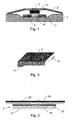
- Fig. 1 an embodiment of a security document according to the invention with a base body 1, an effect sheet 2 and a circuit 3 is shown.
- the circuit 3 is arranged between the main body 1 and the effect foil 2. In other embodiments it can be provided that at least part of the circuit is embedded in the effect foil 2.
- the main body 1 can be made of paper, polymer, composite materials, cotton, plastic, or the like, and is preferably in the form of a thin film or the like.
- the effect foil may comprise a hologram 2, a kinegram, thin-film interference foils, a metallized foil or the like.
- an antenna 4 is arranged, wherein the circuit 3 is connected to the antenna 4. Furthermore, the circuit 3 is arranged in a recess 11 of the main body 1. It seems to be beneficial if the recess 11 is formed as a watermark. The recess 11 may make up about one third to about half of the total thickness of the base body 1.
- the recess 11 of the main body 1 can also be produced by blind embossing. Furthermore, the recess 11 can be introduced by means of punching or perforation in the security document, via which the hologram is applied. In this case, the circuit 3 and / or the antenna 4 can fill out the recess 11 formed as a hole. On the side opposite the hologram 2 side of the security document may optionally be a film application od. Like. Be provided to cover the hole.
- the antenna 4 is arranged between the circuit 3 and the main body 1, that is substantially at the bottom of the recess 11. If the information of the circuit 3 is read from the side facing away from the hologram 2 of the main body 1 Thus, as far as possible an improvement in the transmission and reception properties of the antenna 4 is achieved by this arrangement, whereby the error rate of the system is particularly reduced.
- the circuit may be formed as a chip 3, which has contact points 31 for contacting with the antenna 4.
- the circuit be made independently, whereby a modular structure of the antenna 4, the circuit 3 and the hologram 2 is achieved and in different embodiments, a chip 3 with a different circuit and / or another effect foil 2 can be used in a simple manner.
- the chip 3 is programmable, so that the information stored in it can also be changed after application to the security document. It appears advantageous if only a part of the information can be changed and an identification number or the like is unchangeable.
- the chip 3 and the antenna 4 may be formed in particular as a transponder.
- a hologram 2 which comprises a mirror layer 21, a middle layer 22 and a cover layer 23, wherein the mirror layer 21 is usually made of a metallic material, in particular aluminum.
- a separating layer 24 and a carrier layer 25 are arranged above the covering layer 23, a separating layer 24 and a carrier layer 25 are arranged.
- the carrier layer 25 By means of the carrier layer 25, a plurality of holograms 2 on a coil od. Like. Arranged and stored. After the hologram 2 has been applied to the base body 1, the carrier layer 25 can be separated from the hologram 2 by means of the separating layer 24.
- the antenna 4 is applied to an antenna foil 41.
- the antenna 4 comprises a metal layer 42, which has good conductivity, whereby the antenna 4 can be formed with small dimensions.
- a material of the metal layer 42 copper, gold, silver or the like in particular seem to be suitable.
- the chip 3 is connected to the antenna 4 with an adhesive 32, wherein the contact points 31 are conductively connected to the antenna 4.
- the chip 3 can be produced with the antenna 4 and the antenna foil 41 as a unit.
- Fig. 5 It is shown how the antenna 4 and the chip 3 are embedded in a first adhesive layer 51, wherein the adhesive layer 51 completely covers the chip 3.
- a second adhesive layer 52 is applied, whereupon according to Fig. 7 on the first adhesive layer 51, the hologram 2 is applied to the carrier film 25. Finally, the second adhesive layer 52 is connected to the recess 11 of the base body and the carrier film 25 and the separating layer 24 are separated from the hologram 2.
- first the hologram 2 is applied to the first adhesive layer 51 and then the second adhesive layer 52.
- the in Fig. 7 construction shown can also be done in any other order. With this structure, low accuracy requirements for the positioning of the hologram 2 over the circuit 3 are sufficient.
- the hologram 2 and the circuit 3 can be applied to the base body 1 in one work step, thereby achieving the shortest possible manufacturing time of the security document according to the invention. Furthermore, the hologram 2 for the circuit 3 provides protection against mechanical and / or chemical damage. A mechanical and / or chemical damage to the circuit 3 also results in damage to the hologram 2, which is an optical security feature, which is why such damage immediately noticed.
- the circuit 3 can be applied to this at the end of the manufacturing process of the security document. If the security documents are checked for individual manufacturing steps and defective security documents are eliminated, it can be ensured that only a small amount of security documents occurs after the application of the circuit 3 and the effect foil 2. As a result, the manufacturing cost of the security document according to the invention can be kept low. Furthermore, it is excluded that the circuit 3 and / or the effect film 2 can be damaged in a manufacturing step of the security document according to the invention, since in this manufacturing step, the circuit 3 and the effect sheet 2 are not yet applied to the security document.
- the positioning of the effect foil 2, the circuit 3 and the antenna 4 takes place in a separate step independent of the production of the security document according to the invention, wherein the pre-assembled package effect foil 2, circuit 3 and antenna 4 is applied to the security document according to the invention. This also od a great flexibility in a change of the effect sheet 2, the circuit 3, the shape of the antenna 4. The like. Achieved.
- the presence of the circuit 3 is hidden, these can also be made of any targeted manipulation attempts of the information of the circuit 3.
- the arrangement of the circuit 3 in the recess 11 of the body is achieved that the overall height of the base body 1, the antenna 4, the circuit 3 and the hologram second possibly only slightly protrudes beyond the base body 1 without recess 11, whereby the risk of damage to the hologram 2 and / or the circuit 3 and / or the antenna 4 is reduced.
- the relatively smooth transition between the base body 1 and the hologram 2 appears to be suitable, so that the presence of the circuit 3 remains hidden to most holders of the security document.
- the security document according to the invention is designed as a banknote. If the circuit 3 is designed to be programmable, then the path of a banknote can be traced, which is of particular interest in the fight against crime. Furthermore, cash flow analyzes can provide valuable guidance for economic policy, thereby improving the effectiveness of policy measures and predicting them.
- the circuit 3 is completely hidden, so that the majority of holders of the banknote the presence of the circuit 3 remains hidden. If counterfeiters forge all visible security features, it can still be determined simply and quickly with a reader for the information of the circuit 3 that it is a forgery.
Landscapes
- Physics & Mathematics (AREA)
- General Physics & Mathematics (AREA)
- Engineering & Computer Science (AREA)
- Theoretical Computer Science (AREA)
- Computer Security & Cryptography (AREA)
- Computer Hardware Design (AREA)
- Microelectronics & Electronic Packaging (AREA)
- Credit Cards Or The Like (AREA)
- Inspection Of Paper Currency And Valuable Securities (AREA)
- Transition And Organic Metals Composition Catalysts For Addition Polymerization (AREA)
Description
- Sicherheitsdokument mit einem Grundkörper aus Papier, Polymer, Kompositwerkstoffen od. dgl., einer Effektfolie, insbesondere einem Hologramm od dgl., und einem Schaltkreis, wobei der Schaltkreis zwischen dem Grundkörper und der Effektfolie angeordnet und/oder in der Efiektfolie eingebettet ist, und mit einer zwischen der Effektfolie und dem Grundkörper angeordneten Antenne verbunden ist.
- Es ist bekannt, Sicherheitsdokumente mit Sicherheitsmerkmalen, wie Tiefdruck, Wasserzeichen, Sicherheitsstreifen, Hologrammen, Kinegrammen od. dgl. zu versehen, um die Echtheit eines Sicherheitsdokumentes überprüfen zu können und die Sicherheitsdokumente möglichst fälschungssicher zu gestalten. Dabei ist es üblich, mehrere verschiedene Sicherheitsmerkmale auf einem Sicherheitsdokument anzubringen. Nachteilig an diesen bekannten Sicherheitsdokumenten ist, daß durch das Hinzufügen eines weiteren Sicherheitsmerkmals die Herstellungszeiten und die Herstellungskosten des Sicherheitsdokumentes erhöht werden. Weiters ist bei diesen bekannten Sicherheitsdokumenten nachteilig, daß sie nicht individualisierbar sind und die Merkmale nach der Emission des Sicherheitsdokwnentes nicht adaptiert und/oder upgedatet werden können.
- Die
WO 01/43066 A1 WO 01/43066 A1 - Aus der
EP 1 179 811 A1 geht ein Sicherheitsdokument mit einem Hologramm hervor, bei dem ein Chip in dem Hologramms integriert ist, wobei die Spiegelschicht des Hologramms als Antenne ausgebildet ist. Dadurch, daß das Hologramm als Antenne dient kann die Gesamtbauhöhe im Vergleich zu dem aus derWO 01/43066 A1 EP 1 179 811 A1 ist, daß Aluminium eine geringe Leitfähigkeit aufweist, weshalb es ein schlechtes Antennenmaterial ist, und aufgrund der geringen Dicke der Spiegelschicht die Antenne eine nur geringe Energie aufnehmen kann, wodurch die Reichweite der Antenne gering ist und der Abstand zwischen einem Lesegerät und der Antenne klein sein muß, weshalb das Lesegerät gegenüber der Antenne genau positioniert werden muß. Dadurch wird die Fehleranfälligkeit beim Auslesen der Information des Schaltkreises erhöht, wobei aufgrund eines konstruktionsbedingt nicht unterschreitbaren Abstands ein Auslesen der Information überhaupt unmöglich sein kann. Dieser konstruktionsbedingte Abstand ist z.B. durch die Dicke des Hologramms bestimmt. Ein weiterer Nachteil an dem Sicherheitsdokument gemäß derEP 1 179 811 A1 ist, daß der Chip bei der Herstellung sehr genau gegenüber der Spiegelschicht positioniert werden muß, um eine leitende Verbindung zwischen dem Chip und der Antenne sicherstellen zu können, wodurch die Herstellungskosten erhöht werden. - In der
EP 0 919 950 A1 wird ein Modul für eine IC-Karte, eine IC-Karte, sowie die Herstellung einer IC-Karte beschrieben. Ein mit einer Antenne verbundener Chip wird in einer Ausnehmung der Karte eingesetzt ist, wobei der Chip in der laminierten Karte eingebettet ist. Nachteilig an einer Ausführung gemäß derEP 0 919 950 A1 ist, dass dies zu einem dicken, unflexiblen Aufbau führt. - Die
US 6 111 303 A beschreibt eine Karte mit einem Chip, der in einer Vertiefung einer Grundschicht IC-Karte eingesetzt ist. Dabei ist dieser Chip mit einer Antenne verbunden, die durch Drahtschleifen gebildet ist, wobei die Drahtschleifen zwischen dem Boden der Vertiefung der Karte und dem IC verlaufen und die Vertiefung nach dem Einsetzen des Chips mit einem Harz ausgegossen wird. In einem weiteren Verfahrensschritt wird eine PVC-Schicht auf die Grundschicht aufgeklebt. Nachteilig an einer Ausführung gemäß derUS 6 111 303 A ist, dass dies lediglich zu einem dicken, unflexiblen Aufbau führt, und die große Antennenfläche die durch die Drahtschleifen gebildet wird bei einem durchsichtigen bzw. durchscheinenden Gnmdkörper nicht versteckt werden kann. Damit ist kein, für den Benutzer verborgenes Sicherheitsmerkmal ausführbar. - Aus der
US 6 170 880 B1 geht eine Chipkarte hervor, wobei ein Chip unter einem Hologramm in einer Ausnehmung der Chipkarte angeordnet ist. Weiters ist eine Antenne vorgesehen, wobei die Antenne als im Wesentlichen zwischen der Effektfolie (dem Hologramms) und dem Grundkörper angeordnet ist. Der innere Aufbau einer derartigen Chipkarte führt zu einer großen Bauhöhe und einem unflexiblen Aufbau. Dies macht es weitgehend unmöglich derartige Chipkarten sehr dünn und flexibel auszuführen. - Bei Banknoten ist aus der
DE 196 01 358 C2 bekannt, einen Chip bei der Herstellung des Papiers der Banknoten vollständig in die Papiermasse einzubetten und seine Abmessungen so gering zu wählen, daß eine darauffolgende drucktechnische Verarbeitung möglich ist. Nachteilig an den Banknoten gemäß derDE 196 01 358 C2 ist, daß der Chip, welcher ein kostenintensives Sicherheitsmerkmal darstellt, bereits in der Stufe der Papierherstellung eingebracht wird, wodurch der gesamte Ausschuß, der in den einzelnen Produktionsschritten bis zur fertigen Banknote anfällt auch mit einem Chip versehen ist, wodurch sich hohe Herstellungskosten ergeben, da der gesamte Ausschuß der Produktionskette erfahrungsgemäß bei etwa 20% liegen kann. Außerdem muß die Antenne auf dem Chip angeordnet sein, wodurch sich auch hier die Nachteile eines geringen Energietransfers und demgemäß geringer Reichweite ergebenEP 0905657 offenbart eine Banknote gemäß dem Oberbegriff Anspruchs 1. - Aufgabe der Erfindung ist es daher, ein Sicherheitsdokument der eingangs genannten Art anzugeben, bei dem die Nachteile der bekannten Lösungen vermieden werden. Im besonderen hat sich die Erfindung die Aufgabe gestellt ein Sicherheitsdokument der eingangs genannten Art derart weiterzubilden, daß der Überstand des Chip/Antenne/Hologramm - Elementes über die Oberfläche des Sicherheitsdokumentes gering gehalten werden kann. Auch soll für Aufbringung des Elementes auf das Sicherheitsdokument die Verwendung eines Spezialwerkzeuges vermieden werden. Darüber hinaus soll die Emittierung und das Einspeichern von Daten aus bzw. in den Chip mit möglichst geringem Energieaufwand sicher erzielt werden können. Ferner ist es Aufgabe der Erfindung ein Sicherheitsdokument zu schaffen, bei welchem, die in elektronischer Form gespeicherten Informationen weitgehend vor unerwünschten Manipulationen geschützt sind und der Speicher einen hohen Widerstand gegenüber mechanischen und/oder chemisch bedingten Beschädigungen aufweist.
- Eine weitere Aufgabe der Erfindung ist es, ein Sicherheitsdokument der eingangs genannten Art anzugeben, welches einfach, in möglichst wenigen Arbeitsschritten und ohne großen apparativen Aufwand hergestellt werden kann und bei dem einem Inhaber des Sicherheitsdokumentes wenigstens ein Teil der Sicherheitsmerlanale verborgen bleibt.
- Eine weitere Aufgabe der Erfindung ist es, ein Sicherheitsdokument der eingangs genannten Art anzugeben, welches leicht stapelbar und maschinell verarbeitbar, insbesondere zählbar od. dgl., ist.
- Erfindungsgemäß wird dies dadurch erreicht, dass das Sicherheitsdokument eine Banknote ist. Banknoten stellen Sicherheitsdokumente dar, welche in großer Zahl in Umlauf sind Dabei erscheint es besonders wichtig, wenn einzelne Banknoten schnell und einfach identifiziert werden können, wodurch es möglich ist, Banknoten mit einer vorgebbaren Identifikation zu erkennen. Dies ist insbesondere für Wirtschaftsprognosen und bei der Verbrechensbekämpfung von Interesse. Weiters ergibt sich dadurch der Vorteil, daß der Schaltkreis mit der Antenne und der Effektfolie in einem Arbeitsschritt auf den Grundkörper aufgebracht werden können, sodaß die zur Herstellung eines erfindungsgemäßen Sicherheitsdokumentes erforderlichen Arbeitsschritte weitgehend denen eines bekannten Sicherheitsdokumentes mit einer Effektfolie, z.B. einem Hologramm, ohne Schaltkreis entsprechen. Durch die Effektfolie ist der Schaltkreis und die Antenne weitgehend vor mechanischen und chemisch bedingten Beschädigungen geschützt, wobei für den Schaltkreis keine zusätzlichen Schutzschichten od. dgl, vorgesehen werden müssen. Durch die Anordnung des Schaltkreises in einer Vertiefung des Grundkörpers kann die Gesamtbauhöhe des Grundkörpers, des Schaltkreises mit der Antenne und der Effektfolie gering gehalten werden. Dadurch wird erreicht, daß die Effektfolie nur geringfügig über den Grundkörper hervorsteht oder sogar mit diesem plan abschließen kann, sodaß das erfindungsgemäße Sicherheitsdokument gut stapelbar ist und auch Stapeln von einigen hundert bis tausend Sicherheitsdokumenten hergestellt werden können Weiters wird die Gefahr einer Beschädigung der Effektfolie und/oder des Schaltkreises, insbesondere durch Abscherens verringert. Ein weiterer Vorteil ist, daß die Effektfolie beim Applizieren des Schaltkreises als Träger verwendet werden kann.
- In Weiterbildung der Erfindung kann vorgesehen sein, daß der Schaltkreis als Chip ausgebildet ist. Mit einem Chip ist der Schaltkreis einfach und kostengünstig herstellbar.
- In weiterer Ausgestaltung der Erfindung kann vorgesehen sein, daß der Schaltkreis programmierbar ist. Dadurch können von unterschiedlichen Institutionen Informationen in dem Sicherheitsdokument gespeichert werden, wodurch sich die Geschichte eines Sicherheitsdokumentes rückverfolgen läßt.
- Gemäß einer weiteren Ausführungsform der Erfindung kann vorgesehen sein, daß die Antenne eine Metallschicht, insbesondere aus Kupfer, Gold, Silber od dgl., umfaßt und auf einer Antennenfolie aufgebracht ist. Durch die Antennenfolie kann die Antenne vor Beschädigungen geschützt werden, wobei Kupfer ein guter und kostengünstiger Leiter ist, wodurch die erforderlichen Abmessungen der Antenne aber auch die Signalstärken der Sende-und Empfangssignale der Antenne gering gehalten werden können. Bei der Herstellung kann die Antennenfolie auch als Speichermedium und Träger für mehrere der Antennen und gegebenenfalls die mit diesen verbundenen Schaltkreise dienen.
- In Weiterführung der Erfindung kann vorgesehen sein, daß der Schaltkreis und die Antenne in einer ersten Klebeschicht eingebettet sind. Durch die Einbettung in die erste Klebeschicht können der Schaltkreis und die Antenne auf einfache Weise mit der Effektfolie und/oder dem Grundkörper verbunden werden, wobei die erste Klebeschicht zusätzlich eine Schutzschicht für den Schaltkreis und die Antenne darstellt.
- In weiterer Ausgestaltung der Erfindung kann vorgesehen sein, daß die Antenne zwischen dem Schaltkreis und dem Grundkörper angeordnet ist. Werden die Informationen des Schaltkreises von der der Effektfolie abgewandten Seite des Grundkörpers ausgelesen, so wird durch diese Anordnung eine möglichst große Reichweite wie überhaupt eine Verbesserung der Sende- und Empfangseigenschaften der Antenne erreicht, wodurch insbesondere die Fehleranfälligkeit des Systems verringert wird.
- Die Erfindung betrifft weiters eine Verfahren zur Herstellung eines erfindungsgemäßen Sicherheitsdokumentes mit einem Grundkörper aus Papier od. dgl..
- Aufgabe der Erfindung ist es, ein Verfahren anzugeben, bei dem das oben angeführte Sicherheitsdokument auf einfache Weise und kostengünstig hergestellt werden kann. Erfindungsgemäß wird dies dadurch erreicht, daß auf eine Antennenfolie mit einer Metallschicht, insbesondere Kupfer, Gold, Silber od. dgl. umfassend, ein die Metallschicht kontaktierender Chip befestigt wird, der Chip in eine erste Klebstoffschicht eingebettet wird, auf die erste Klebstoffschicht eine EfiektfoGe, insbesondere ein Hologramm od. dgl., aufgebracht wird, auf die der Metallschicht gegenüberliegenden Seite der Antennenfolie eine zweite Klebstoffischicht aufgebracht wird und die zweite Klebstoffschicht mit einer Vertiefung des Grundkörpers verbunden wird. Dadurch ergibt sich der Vorteil, daß die Effektfolie und der Chip in einem Arbeitsschritt auf den Grundkörper aufgebracht werden können, wodurch die Herstellungszeit des erfindungsgemäßen Sicherheitsdokuments gering gehalten wird. Weiters kann die Effektfolie und der Chip in einem der letzten Arbeitsschritte bei der Herstellung des Sicherheitsdokumentes auf dieses aufgebracht werden, wobei der Ausschuß der vorhergehenden Produktionskette vorher ausgesondert werden kann, wodurch die Herstellungskosten des Sicherheitsdokumentes möglichst gering gehalten werden können. Weiters kann es bei vorhergehenden Arbeitsschritten, insbesondere bei der Anwendung eines Tiefdruckverfahrens, erforderlich sein hohe Drücke auf das Sicherheitsdokument aufzubringen. Durch das nachfolgende Applizieren des Chips ist es nicht erforderlich, diese Arbeitsschritten unter Berücksichtigung der Gefahr einer Beschädigung eines bereits applizierten Chips auszugestalten, wodurch diese Arbeitsschritte einfacher und kostengünstiger ausgestaltet werden können. Ein weiterer Vorteil ist, daß die Effektfolie den Grundköper gegebenenfalls nur geringfügig überragt, wodurch die Gefahr einer Beschädigung der Effektfolie und/oder des Chips, insbesondere durch Abscheren, verringert wird. Die Aufgaben werden gelöst durch die Erfindung gemäß Anspruch 1 und Anspruch 7.
- Die Erfindung wird unter Bezugnahme auf die beigeschlossenen Zeichnungen, in welchen Ausführungsformen dargestellt sind, näher beschrieben. Dabei zeigt:
-
Fig. 1 eine Ausführungsform eines erfindungsgemäßen Sicherheitsdokumentes; -
Fig. 2 einen einen Schaltkreis enthaltenden Chip der Ausführungsform gemäßFig. 1 ; -
Fig. 3 ein Hologramm der Ausführungsform gemäßFig. 1 , welches mit einer Trägerfolie verbunden ist; -
Fig.4 eine Antennenfolie mit Antennen, wobei mit jeweils einer Antenne ein Chip verbunden ist; -
Fig. 5 die Antennenfolie gemäßFig. 4 , wobei eine erste Klebeschicht auf die Antennenfolie aufgebracht wird; Weiter mit Seite 6 -
Fig. 6 die Antennenfolie gemäßFig. 5 , wobei auf die der Antenne gegenüberliegende Seite eine zweite Klebeschicht aufgebracht ist; und -
Fig. 7 die Antennenfolie gemäßFig. 6 , wobei auf die erste Klebeschicht ein Hologramm mit einer Trägerfolie aufgebracht ist. - In
Fig. 1 ist eine Ausführungsform eines erfindungsgemäßen Sicherheitsdokumentes mit einem Grundkörper 1, einer Effektfolie 2 und einem Schaltkreis 3 dargestellt. Der Schaltkreis 3 ist zwischen dem Grundkörper 1 und der Effektfolie 2 angeordnet. Bei anderen Ausfiihrungsformen kann vorgesehen sein, daß zumindest ein Teil des Schaltkreises in der Effektfolie 2 eingebettet ist. - Der Grundkörper 1 kann aus Papier, Polymer, Kompositwerkstoffen, Baumwolle, Kunststoff, od. dgl. sein und ist vorzugsweise als dünne Folie od. dgl. ausgebildet. Die Effektfolie kann ein Hologramm 2, ein Kinegramm, Dünnschichtinterferenzfolien, eine metallisierte Folie od. dgl. umfassen.
- Zwischen dem Hologramm 2 und dem Grundkörper 1 ist eine Antenne 4 angeordnet, wobei der Schaltkreis 3 mit der Antenne 4 verbunden ist. Weiters ist der Schaltkreis 3 in einer Vertiefung 11 des Grundkörpers 1 angeordnet. Dabei erscheint es günstig zu sein, wenn die Vertiefung 11 als Wasserzeichen ausgebildet ist. Die Vertiefung 11 kann etwa ein Drittel bis etwa die Hälfte der Gesamtdicke des Grundkörpers 1 ausmachen.
- Die Vertiefung 11 des Grundkörpers 1 kann auch durch Blindprägung erzeugt werden. Weiters kann die Vertiefung 11 mittels Stanzung oder Perforation in das Sicherheitsdokument eingebracht werden, über das das Hologramm appliziert wird. Dabei kann der Schaltkreis 3 und/oder die Antenne 4 die als Loch ausgebildete Vertiefung 11 ausfüllen. Auf der dem Hologramm 2 gegenüberliegenden Seite des Sicherheitsdokumentes kann gegebenenfalls eine Folienapplikation od. dgl. zur Abdeckung des Lochs vorgesehen sein.
- In diesem Zusammenhang erscheint es günstig zu sein, wenn die Antenne 4 zwischen dem Schaltkreis 3 und dem Grundkörper 1 angeordnet ist, also im wesentlichen am Boden der Vertiefung 11. Werden die Informationen des Schaltkreises 3 von der dem Hologramm 2 abgewandten Seite des Grundkörpers 1 ausgelesen, so wird durch diese Anordnung eine möglichst große Reichweite wie überhaupt eine Verbesserung der Sende- und Empfangseigenschaften der Antenne 4 erreicht, wodurch insbesondere die Fehleranfälligkeit des Systems verringert wird.
- Gemäß
Fig. 2 kann der Schaltkreis als Chip 3 ausgebildet sein, welcher Kontaktstellen 31 für die Kontaktierung mit der Antenne 4 aufweist. Mittels des Chips 3 kann der Schaltkreis eigenständig hergestellt werden, wodurch ein modularer Aufbau der Antenne 4, des Schaltkreises 3 und des Hologramms 2 erreicht wird und bei unterschiedlichen Ausführungsformen auf einfache Weise ein Chip 3 mit einem anderem Schaltkreis und/oder eine andere Effektfolie 2 verwendet werden kann. Weiters kann vorgesehen sein, daß der Chip 3 programmierbar ist, sodaß die in ihm gespeicherte Information auch nach dem Aufbringen auf das Sicherheitsdokument verändert werden kann. Dabei erscheint es vorteilhaft, wenn nur ein Teil der Information verändert werden kann und eine Identifikationsnummer od. dgl. unveränderbar ist. Der Chip 3 und die Antenne 4 können insbesondere als Transponder ausgebildet sein. - In
Fig. 3 ist schematisch ein Hologramm 2 dargestellt, welches eine Spiegelschicht 21, eine Mittelschicht 22 und eine Deckschicht 23 umfaßt, wobei die Spiegelschicht 21 üblicherweise aus einem metallischen Material, insbesondere Aluminium, ist. Oberhalb der Deckschicht 23 ist eine Trennschicht 24 und eine Trägerschicht 25 angeordnet. Mittels der Trägerschicht 25 können mehrere Hologramme 2 auf einer Spule od. dgl. angeordnet und gelagert werden. Nach dem Aufbringen des Hologramms 2 auf den Grundkörper 1 kann die Trägerschicht 25 mittels der Trennschicht 24 vom Hologramm 2 getrennt werden. - In den
Fig. 4 bis 7 ist ein Teil eines Herstellungsverfahrens des erfindungsgemäßen Sicherheitsdokumentes dargestellt. GemäßFig. 4 ist dabei die Antenne 4 auf einer Antennenfolie 41 aufgebracht. Durch die Antennenfolie sind die Antennen 4 gleichmäßig voneinander beabstandet und können auf einfache Weise mehrere Antennen 4 manipuliert werden. Die Antenne 4 umfaßt eine Metallschicht 42, welche eine gute Leitfähigkeit aufweist, wodurch die Antenne 4 mit geringen Abmessungen ausgebildet werden kann. Als Material der Metallschicht 42 scheinen insbesondere Kupfer, Gold, Silber od. dgl. geeignet zu sein. Der Chip 3 ist mit einem Klebemittel 32 mit der Antenne 4 verbunden, wobei die Kontaktstellen 31 leitend mit der Antenne 4 verbunden sind. Der Chip 3 kann mit der Antenne 4 und der Antennenfolie 41 als Einheit produziert werden. - In
Fig. 5 ist gezeigt, wie die Antenne 4 und der Chip 3 in eine erste Klebeschicht 51 eingebettet werden, wobei die Klebeschicht 51 den Chip 3 vollständig bedeckt. - Auf die der Antenne 4 gegenüberliegende Seite der Antennenfolie 41 wird gemäß
Fig. 6 eine zweite Klebeschicht 52 aufgebracht, woraufhin gemäßFig. 7 auf die erste Klebeschicht 51 das Hologramm 2 mit der Trägerfolie 25 aufgebracht wird. Abschließend wird die zweite Klebeschicht 52 mit der Vertiefung 11 des Grundkörpers verbunden und die Trägerfolie 25 und die Trennschicht 24 von dem Hologramm 2 getrennt. - In anderen Ausführungsformen kann auch vorgesehen sein, daß zuerst das Hologramm 2 auf die erste Klebeschicht 51 und anschließend die zweite Klebeschicht 52 aufgebracht wird. Der in
Fig. 7 gezeigte Aufbau kann aber auch in jeder anderen Reihenfolge erfolgen. Bei diesem Aufbau sind geringe Genauigkeitsanforderungen an die Positionierung des Hologramms 2 über dem Schaltkreis 3 ausreichend. - Vorteilhaft erscheint, daß das Hologramm 2 und der Schaltkreis 3 in einem Arbeitsschritt auf den Grundkörper 1 aufgebracht werden können, wodurch eine möglichst geringe Herstellungszeit des erfindungsgemäßen Sicherheitsdokumentes erreicht wird. Weiters bildet das Hologramm 2 für den Schaltkreis 3 einen Schutz vor mechanischer und/oder chemisch bedingter Beschädigung. Eine mechanisch und/oder chemisch bedingte Beschädigung des Schaltkreises 3 hat auch eine Beschädigung des Hologramms 2 zur Folge, welche ein optisches Sicherheitsmerkmal darstellt, weshalb eine solche Beschädigung sofort auffällt.
- Bei diesem erfindungsgemäßen Verfahren kann der Schaltkreis 3 am Ende des Herstellungsverfahrens des Sicherheitsdokumentes auf dieses aufgebracht werden. Werden die Sicherheitsdokumente nach einzelnen Herstellungsschritten überprüft und fehlerhafte Sicherheitsdokumente ausgeschieden, so kann sichergestellt werden, daß ein nur geringer Ausschuss an Sicherheitsdokumenten nach dem Aufbringen des Schaltkreises 3 und der Effektfolie 2 auftritt. Dadurch können die Herstellungskosten des erfindungsgemäßen Sicherheitsdokumentes gering gehalten werden. Weiters wird ausgeschlossen, daß der Schaltkreis 3 und/oder die Effektfolie 2 bei einem Herstellungsschritt des erfindungsgemäßen Sicherheitsdokumentes beschädigt werden können, da bei diesem Herstellungsschritt der Schaltkreis 3 und die Effektfolie 2 noch nicht auf das Sicherheitsdokument aufgebracht sind.
- Die Positionierung der Effektfolie 2, des Schaltkreises 3 und der Antenne 4 erfolgt in einem eigenen Arbeitsschritt unabhängig von der Herstellung des erfindungsgemäßen Sicherheitsdokumentes, wobei das vorassemblierte Package Effektfolie 2, Schaltkreis 3 und Antenne 4 auf das erfindungsgemäße Sicherheitsdokument aufgebracht wird. Dadurch wird auch eine große Flexibilität bei einer Änderung der Effektfolie 2, des Schaltkreises 3, der Form der Antenne 4 od. dgl. erreicht.
- Da den meisten Inhabern des Sicherheitsdokumentes das Vorhandensein des Schaltkreises 3 verborgen bleibt, können von diesen auch keine gezielten Manipulationsversuche der Information des Schaltkreises 3 vorgenommen werden. Durch die Anordnung des Schaltkreises 3 in der Vertiefung 11 des Grundkörpers wird erreicht, daß die Gesamtbauhöhe des Grundkörpers 1, der Antenne 4, des Schaltkreises 3 und des Hologramms 2 gegebenenfalls nur geringfügig über den Grundkörper 1 ohne Vertiefung 11 hinausragt, wodurch die Gefahr einer Beschädigung des Hologramms 2 und/oder des Schaltkreises 3 und/oder der Antenne 4 verringert wird. Weiters erscheint der relativ glatte Übergang zwischen dem Grundkörper 1 und dem Hologramm 2 geeignet zu sein, damit das Vorhandensein des Schaltkreises 3 den meisten Inhabern des Sicherheitsdokuments verborgen bleibt.
- Das erfindungsgemäße Sicherheitsdokument ist als Banknote ausgebildet. Ist der Schaltkreis 3 programmierbar ausgeführt, so kann der Weg einer Banknote zurückverfolgt werden, was insbesondere bei der Verbrechensbekämpfung von Interesse ist. Weiters können mittels Geldflußanalysen wertvolle Hinweise für die Wirtschaftspolitik erstellt werden und dadurch die Effizienz von politischen Maßnahmen besser überprüft und vorhergesagt werden.
- Durch das Hologramm 2 ist der Schaltkreis 3 vollständig verdeckt, sodaß den meisten Inhabern der Banknote das Vorhandensein des Schaltkreises 3 verborgen bleibt. Werden von Fälschern alle sichtbaren Sicherheitsmerkmale gefälscht, so kann dennoch mit einem Lesegerät für die Information des Schaltkreises 3 einfach und schnell festgestellt werden, daß es sich um eine Fälschung handelt.
Claims (7)
- Banknote mit einem Grundkörper (1) aus Papier, Polymer, Kompositwerkstoffen od. dgl., einer Effektfolie (2), insbesondere einem Hologramm od. dgl., und einem Schaltkreis (3), wobei der Schaltkreis (3) zwischen dem Grundkörper (1) und der Effektfolie (2) angeordnet und/oder in der Effektfolie (2) eingebettet ist, und mit einer zwischen der Effektfolie (2) und dem Grundkörper (1) angeordneten Antenne (4) verbunden ist, dadurch gekennzeichnet, daß der Schaltkreis (3) in einer Vertiefung (11) des Grundkörpers (1), insbesondere einem Wasserzeichen od. dgl., angeordnet ist.
- Banknote nach Anspruch 1, dadurch gekennzeichnet, dass der Schaltkreis als Chip (3) ausgebildet ist.
- Banknote nach Anspruch 1 oder 2, dadurch gekennzeichnet, daß der Schaltkreis (3) programmierbar ist.
- Banknote nach Anspruch 1, 2 oder 3, dadurch gekennzeichnet, dass die Antenne (4) eine Metallschicht (42), insbesondere aus Kupfer, Gold, Silber od. dgl., umfasst und auf einer Antennenfolie (41) aufgebracht ist.
- Banknote nach einem der Ansprüche 1 bis 4, dadurch gekennzeichnet. dass der Schaltkreis (3) und die Antenne (4) in einer ersten Klebeschicht (51) eingebettet sind.
- Banknote nach einem der Anspräche 1 bis 5, dadurch gekennzeichnet, dass die Antenne (4) zwischen dem Schaltkreis (2) und dem Grundkörper (1) angeordnet ist.
- Verfahren zur Herstellung einer Banknote nach einem der Ansprüche 1 bis 6, dadurch gekennzeichnet, dass auf eine. Antennenfolie (41) mit einer Metallschicht (42), insbesondere Kupfer, Gold, Silber od. dgl. umfassend, ein die Metallschicht (42) kontaktierender Chip (3) befestigt wird, der Chip (3) in eine erste Klebstoffschicht (51) eingebettet wird, auf die erste Klebstoffschicht (51) eine Effektfolie (2), insbesondere ein Hologramm od. dgl.. aufgebracht wird, auf die der Metallschicht (42) gegenüberliegenden Seite der Antennenfolie (41) eine zweite Klebstoffschicht (52) aufgebracht wird und die zweite Klebstoffschicht (52) mit einer Vertiefung (11) des Grundkörpers (1) verbunden wird.
Priority Applications (1)
| Application Number | Priority Date | Filing Date | Title |
|---|---|---|---|
| AT03763504T ATE424594T1 (de) | 2002-07-17 | 2003-07-16 | Sicherheitsdokument |
Applications Claiming Priority (3)
| Application Number | Priority Date | Filing Date | Title |
|---|---|---|---|
| AT10782002 | 2002-07-17 | ||
| AT10782002 | 2002-07-17 | ||
| PCT/AT2003/000200 WO2004008397A1 (de) | 2002-07-17 | 2003-07-16 | Sicherheitsdokument |
Publications (3)
| Publication Number | Publication Date |
|---|---|
| EP1525564A1 EP1525564A1 (de) | 2005-04-27 |
| EP1525564B1 true EP1525564B1 (de) | 2009-03-04 |
| EP1525564B2 EP1525564B2 (de) | 2012-08-22 |
Family
ID=30120909
Family Applications (1)
| Application Number | Title | Priority Date | Filing Date |
|---|---|---|---|
| EP03763504A Expired - Lifetime EP1525564B2 (de) | 2002-07-17 | 2003-07-16 | Verfahren zur herstellung einer banknote |
Country Status (6)
| Country | Link |
|---|---|
| EP (1) | EP1525564B2 (de) |
| AT (1) | ATE424594T1 (de) |
| AU (1) | AU2003246446A1 (de) |
| DE (1) | DE50311245D1 (de) |
| ES (1) | ES2324217T5 (de) |
| WO (1) | WO2004008397A1 (de) |
Families Citing this family (6)
| Publication number | Priority date | Publication date | Assignee | Title |
|---|---|---|---|---|
| ATE367938T1 (de) * | 2004-04-27 | 2007-08-15 | Bundesdruckerei Gmbh | Sicherheitsmerkmal für datenträger, entsprechender datenträger und verfahren zur herstellung eines sicherheitsmerkmals |
| DE102004031879B4 (de) | 2004-06-30 | 2017-11-02 | Ovd Kinegram Ag | Sicherheitsdokument zur RF-Identifikation |
| FR2932910B1 (fr) * | 2008-06-20 | 2011-02-11 | Smart Packaging Solutions Sps | Carte sans contact avec logo securitaire |
| FR2932908B1 (fr) * | 2008-06-24 | 2012-11-16 | Arjowiggins Licensing Sas | Structure comportant un filigrane ou pseudo-filigrane et un dispositif a microcircuit integre. |
| JP5113727B2 (ja) * | 2008-11-20 | 2013-01-09 | 株式会社日立製作所 | 無線icタグ |
| EP2264652B1 (de) | 2009-06-09 | 2016-06-01 | Ricoh Company, Ltd. | Umkehrbares wärmeempfindliches Aufzeichnungsmedium und Verfahren zu seiner Herstellung |
Family Cites Families (11)
| Publication number | Priority date | Publication date | Assignee | Title |
|---|---|---|---|---|
| YU48550B (sh) † | 1990-07-06 | 1998-11-05 | Pipelife Rohrsysteme Gesellschaft M.B.H. | Sigurnosni uređaj za zatvaranje gasnih cevovoda sa ventilom |
| DE4334847A1 (de) † | 1993-10-13 | 1995-04-20 | Kurz Leonhard Fa | Wertdokument mit Fenster |
| DE59604925D1 (de) * | 1996-07-15 | 2000-05-11 | Austria Card | Datenträger mit einem modul und einem hologramm |
| US5944927A (en) † | 1997-05-29 | 1999-08-31 | The Standard Register Company | Security paper having an embedded security thread and a process for making the security paper |
| WO1998059317A1 (en) * | 1997-06-23 | 1998-12-30 | Rohm Co., Ltd. | Module for ic card, ic card, and method for manufacturing module for ic card |
| DE69722403T2 (de) † | 1997-09-23 | 2004-01-15 | St Microelectronics Srl | Banknote mit einer integrierten Schaltung |
| FR2769441A1 (fr) * | 1997-10-07 | 1999-04-09 | Philips Electronics Nv | Carte electronique sans contact et son procede de fabrication |
| NL1008929C2 (nl) † | 1998-04-20 | 1999-10-21 | Vhp Ugchelen Bv | Uit papier vervaardigd substraat voorzien van een geïntegreerde schakeling. |
| FR2802001B1 (fr) * | 1999-12-06 | 2002-01-18 | Gemplus Card Int | Corps support d'information comprenant un element de securite comportant une puce de circuit integre |
| DE10032128A1 (de) † | 2000-07-05 | 2002-01-17 | Giesecke & Devrient Gmbh | Sicherheitspapier und daraus hergestelltes Wertdokument |
| FR2832354B1 (fr) † | 2001-11-20 | 2004-02-20 | Arjo Wiggins Sa | Procede de fabrication d'un article comportant une feuille et au moins un element rapporte sur cette feuille |
-
2003
- 2003-07-16 EP EP03763504A patent/EP1525564B2/de not_active Expired - Lifetime
- 2003-07-16 AU AU2003246446A patent/AU2003246446A1/en not_active Abandoned
- 2003-07-16 ES ES03763504T patent/ES2324217T5/es not_active Expired - Lifetime
- 2003-07-16 DE DE50311245T patent/DE50311245D1/de not_active Expired - Lifetime
- 2003-07-16 WO PCT/AT2003/000200 patent/WO2004008397A1/de not_active Ceased
- 2003-07-16 AT AT03763504T patent/ATE424594T1/de active
Also Published As
| Publication number | Publication date |
|---|---|
| WO2004008397A1 (de) | 2004-01-22 |
| EP1525564B2 (de) | 2012-08-22 |
| AU2003246446A1 (en) | 2004-02-02 |
| DE50311245D1 (de) | 2009-04-16 |
| ES2324217T5 (es) | 2012-12-27 |
| ES2324217T3 (es) | 2009-08-03 |
| ATE424594T1 (de) | 2009-03-15 |
| EP1525564A1 (de) | 2005-04-27 |
Similar Documents
| Publication | Publication Date | Title |
|---|---|---|
| EP2672431B1 (de) | Datenträger mit Transponder | |
| DE69904163T2 (de) | Aus papier gefertigtes substrat mit einem integrierten schaltkreis | |
| DE102004008841A1 (de) | Verfahren zur Herstellung einer Buchdeckeneinlage und eines buchartigen Wertdokuments sowie eine Buchdeckeneinlage und ein buchartiges Wertdokument | |
| EP0835497B1 (de) | Chipkarte | |
| EP2452826B1 (de) | Foliensicherheitselement mit Durchbrechungsbereich | |
| WO2000007151A1 (de) | Sicherheitspapier sowie verfahren und vorrichtung zur prüfung der echtheit darauf aufgezeichneter urkunden | |
| DE102004008840A1 (de) | Verfahren zur Herstellung eines buchartigen Wertdokuments sowie ein buchartiges Wertdokument | |
| DE19601358A1 (de) | Grundmaterial | |
| EP3262570A2 (de) | Mehrschichtkörper und sicherheitsdokument | |
| EP1603757B1 (de) | Verfahren zur herstellung einer buchdeckeneinlage und eines buchartigen wertdokumentes sowie eine buchdeckeneinlage und ein buchartiges wertdokument | |
| DE102007040865A1 (de) | Sicherheitspapier | |
| EP1527413B1 (de) | Datenträger mit transponderspule | |
| EP1525564B1 (de) | Sicherheitsdokument | |
| EP1169179B2 (de) | Aufzeichnungsträger und verfahren zu seiner herstellung | |
| EP3741580B1 (de) | Wert- oder sicherheitsdokument sowie verfahren zu dessen herstellung | |
| WO2004109590A2 (de) | Datenträger und herstellungsverfahren | |
| EP2819846B1 (de) | Dokument und verfahren zum herstellen des dokuments | |
| DE60001163T2 (de) | Sicherheitsanordnung und ihre verwendungen | |
| EP2919170B1 (de) | Verfahren zum Herstellen eines Datenträgers | |
| DE102005053251A1 (de) | Flächenhaftes Substrat für ein biometrisches Merkmal und Verfahren zur Herstellung des Substrats | |
| WO2007054264A1 (de) | Flächenhaftes substrat für informationsaufzeichnung und verfahren zur herstellung des substrats | |
| DE102014014627A1 (de) | Verfahren zum Herstellen eines Transponders und Transponder | |
| DE102006009999A1 (de) | Flächenhaftes Substrat zur Aufzeichnung von Binärwerten und Verfahren zur Herstellung des Substrats |
Legal Events
| Date | Code | Title | Description |
|---|---|---|---|
| PUAI | Public reference made under article 153(3) epc to a published international application that has entered the european phase |
Free format text: ORIGINAL CODE: 0009012 |
|
| 17P | Request for examination filed |
Effective date: 20050217 |
|
| AK | Designated contracting states |
Kind code of ref document: A1 Designated state(s): AT BE BG CH CY CZ DE DK EE ES FI FR GB GR HU IE IT LI LU MC NL PT RO SE SI SK TR |
|
| AX | Request for extension of the european patent |
Extension state: AL LT LV MK |
|
| DAX | Request for extension of the european patent (deleted) | ||
| RIN1 | Information on inventor provided before grant (corrected) |
Inventor name: SCHWARZBACH, DANIEL Inventor name: FAJMANN, PETER Inventor name: DEINHAMMER, HARALD |
|
| GRAP | Despatch of communication of intention to grant a patent |
Free format text: ORIGINAL CODE: EPIDOSNIGR1 |
|
| GRAS | Grant fee paid |
Free format text: ORIGINAL CODE: EPIDOSNIGR3 |
|
| GRAA | (expected) grant |
Free format text: ORIGINAL CODE: 0009210 |
|
| AK | Designated contracting states |
Kind code of ref document: B1 Designated state(s): AT BE BG CH CY CZ DE DK EE ES FI FR GB GR HU IE IT LI LU MC NL PT RO SE SI SK TR |
|
| REG | Reference to a national code |
Ref country code: GB Ref legal event code: FG4D Free format text: NOT ENGLISH |
|
| REG | Reference to a national code |
Ref country code: CH Ref legal event code: EP |
|
| REG | Reference to a national code |
Ref country code: IE Ref legal event code: FG4D Free format text: LANGUAGE OF EP DOCUMENT: GERMAN |
|
| REF | Corresponds to: |
Ref document number: 50311245 Country of ref document: DE Date of ref document: 20090416 Kind code of ref document: P |
|
| REG | Reference to a national code |
Ref country code: SE Ref legal event code: TRGR |
|
| REG | Reference to a national code |
Ref country code: CH Ref legal event code: NV Representative=s name: BOVARD AG PATENTANWAELTE |
|
| PG25 | Lapsed in a contracting state [announced via postgrant information from national office to epo] |
Ref country code: FI Free format text: LAPSE BECAUSE OF FAILURE TO SUBMIT A TRANSLATION OF THE DESCRIPTION OR TO PAY THE FEE WITHIN THE PRESCRIBED TIME-LIMIT Effective date: 20090304 Ref country code: SI Free format text: LAPSE BECAUSE OF FAILURE TO SUBMIT A TRANSLATION OF THE DESCRIPTION OR TO PAY THE FEE WITHIN THE PRESCRIBED TIME-LIMIT Effective date: 20090304 |
|
| REG | Reference to a national code |
Ref country code: ES Ref legal event code: FG2A Ref document number: 2324217 Country of ref document: ES Kind code of ref document: T3 |
|
| REG | Reference to a national code |
Ref country code: IE Ref legal event code: FD4D |
|
| PG25 | Lapsed in a contracting state [announced via postgrant information from national office to epo] |
Ref country code: CZ Free format text: LAPSE BECAUSE OF FAILURE TO SUBMIT A TRANSLATION OF THE DESCRIPTION OR TO PAY THE FEE WITHIN THE PRESCRIBED TIME-LIMIT Effective date: 20090304 Ref country code: EE Free format text: LAPSE BECAUSE OF FAILURE TO SUBMIT A TRANSLATION OF THE DESCRIPTION OR TO PAY THE FEE WITHIN THE PRESCRIBED TIME-LIMIT Effective date: 20090304 Ref country code: PT Free format text: LAPSE BECAUSE OF FAILURE TO SUBMIT A TRANSLATION OF THE DESCRIPTION OR TO PAY THE FEE WITHIN THE PRESCRIBED TIME-LIMIT Effective date: 20090819 Ref country code: IE Free format text: LAPSE BECAUSE OF FAILURE TO SUBMIT A TRANSLATION OF THE DESCRIPTION OR TO PAY THE FEE WITHIN THE PRESCRIBED TIME-LIMIT Effective date: 20090304 |
|
| PG25 | Lapsed in a contracting state [announced via postgrant information from national office to epo] |
Ref country code: SK Free format text: LAPSE BECAUSE OF FAILURE TO SUBMIT A TRANSLATION OF THE DESCRIPTION OR TO PAY THE FEE WITHIN THE PRESCRIBED TIME-LIMIT Effective date: 20090304 Ref country code: RO Free format text: LAPSE BECAUSE OF FAILURE TO SUBMIT A TRANSLATION OF THE DESCRIPTION OR TO PAY THE FEE WITHIN THE PRESCRIBED TIME-LIMIT Effective date: 20090304 |
|
| PLBI | Opposition filed |
Free format text: ORIGINAL CODE: 0009260 |
|
| PLAX | Notice of opposition and request to file observation + time limit sent |
Free format text: ORIGINAL CODE: EPIDOSNOBS2 |
|
| 26 | Opposition filed |
Opponent name: DE LA RUE INTERNATIONAL LIMITED Effective date: 20091203 |
|
| PG25 | Lapsed in a contracting state [announced via postgrant information from national office to epo] |
Ref country code: DK Free format text: LAPSE BECAUSE OF FAILURE TO SUBMIT A TRANSLATION OF THE DESCRIPTION OR TO PAY THE FEE WITHIN THE PRESCRIBED TIME-LIMIT Effective date: 20090304 |
|
| BERE | Be: lapsed |
Owner name: OESTERREICHISCHE BANKNOTEN- UND SICHERHEITSDRUCK Effective date: 20090731 |
|
| PG25 | Lapsed in a contracting state [announced via postgrant information from national office to epo] |
Ref country code: MC Free format text: LAPSE BECAUSE OF NON-PAYMENT OF DUE FEES Effective date: 20090731 |
|
| NLR1 | Nl: opposition has been filed with the epo |
Opponent name: DE LA RUE INTERNATIONAL LIMITED |
|
| PLAF | Information modified related to communication of a notice of opposition and request to file observations + time limit |
Free format text: ORIGINAL CODE: EPIDOSCOBS2 |
|
| PG25 | Lapsed in a contracting state [announced via postgrant information from national office to epo] |
Ref country code: BE Free format text: LAPSE BECAUSE OF NON-PAYMENT OF DUE FEES Effective date: 20090731 |
|
| PLBB | Reply of patent proprietor to notice(s) of opposition received |
Free format text: ORIGINAL CODE: EPIDOSNOBS3 |
|
| PLBP | Opposition withdrawn |
Free format text: ORIGINAL CODE: 0009264 |
|
| PG25 | Lapsed in a contracting state [announced via postgrant information from national office to epo] |
Ref country code: GR Free format text: LAPSE BECAUSE OF FAILURE TO SUBMIT A TRANSLATION OF THE DESCRIPTION OR TO PAY THE FEE WITHIN THE PRESCRIBED TIME-LIMIT Effective date: 20090605 |
|
| PLAY | Examination report in opposition despatched + time limit |
Free format text: ORIGINAL CODE: EPIDOSNORE2 |
|
| PG25 | Lapsed in a contracting state [announced via postgrant information from national office to epo] |
Ref country code: IT Free format text: LAPSE BECAUSE OF FAILURE TO SUBMIT A TRANSLATION OF THE DESCRIPTION OR TO PAY THE FEE WITHIN THE PRESCRIBED TIME-LIMIT Effective date: 20090304 |
|
| REG | Reference to a national code |
Ref country code: CH Ref legal event code: PFA Owner name: OESTERREICHISCHE BANKNOTEN- UND SICHERHEITSDRUCK Free format text: OESTERREICHISCHE BANKNOTEN- UND SICHERHEITSDRUCK GMBH#GARNISONGASSE 15#1096 WIEN (AT) -TRANSFER TO- OESTERREICHISCHE BANKNOTEN- UND SICHERHEITSDRUCK GMBH#GARNISONGASSE 15#1096 WIEN (AT) |
|
| PLBC | Reply to examination report in opposition received |
Free format text: ORIGINAL CODE: EPIDOSNORE3 |
|
| PLAY | Examination report in opposition despatched + time limit |
Free format text: ORIGINAL CODE: EPIDOSNORE2 |
|
| PG25 | Lapsed in a contracting state [announced via postgrant information from national office to epo] |
Ref country code: LU Free format text: LAPSE BECAUSE OF NON-PAYMENT OF DUE FEES Effective date: 20090716 |
|
| PG25 | Lapsed in a contracting state [announced via postgrant information from national office to epo] |
Ref country code: HU Free format text: LAPSE BECAUSE OF FAILURE TO SUBMIT A TRANSLATION OF THE DESCRIPTION OR TO PAY THE FEE WITHIN THE PRESCRIBED TIME-LIMIT Effective date: 20090905 |
|
| PLBC | Reply to examination report in opposition received |
Free format text: ORIGINAL CODE: EPIDOSNORE3 |
|
| PLAY | Examination report in opposition despatched + time limit |
Free format text: ORIGINAL CODE: EPIDOSNORE2 |
|
| PLBC | Reply to examination report in opposition received |
Free format text: ORIGINAL CODE: EPIDOSNORE3 |
|
| PG25 | Lapsed in a contracting state [announced via postgrant information from national office to epo] |
Ref country code: CY Free format text: LAPSE BECAUSE OF FAILURE TO SUBMIT A TRANSLATION OF THE DESCRIPTION OR TO PAY THE FEE WITHIN THE PRESCRIBED TIME-LIMIT Effective date: 20090304 |
|
| PLAY | Examination report in opposition despatched + time limit |
Free format text: ORIGINAL CODE: EPIDOSNORE2 |
|
| PLBC | Reply to examination report in opposition received |
Free format text: ORIGINAL CODE: EPIDOSNORE3 |
|
| RTI2 | Title (correction) |
Free format text: METHOD FOR PRODUCING A BANKNOTE |
|
| PUAH | Patent maintained in amended form |
Free format text: ORIGINAL CODE: 0009272 |
|
| STAA | Information on the status of an ep patent application or granted ep patent |
Free format text: STATUS: PATENT MAINTAINED AS AMENDED |
|
| 27A | Patent maintained in amended form |
Effective date: 20120822 |
|
| AK | Designated contracting states |
Kind code of ref document: B2 Designated state(s): AT BE BG CH CY CZ DE DK EE ES FI FR GB GR HU IE IT LI LU MC NL PT RO SE SI SK TR |
|
| REG | Reference to a national code |
Ref country code: CH Ref legal event code: AEN Free format text: AUFRECHTERHALTUNG DES PATENTES IN GEAENDERTER FORM |
|
| REG | Reference to a national code |
Ref country code: DE Ref legal event code: R102 Ref document number: 50311245 Country of ref document: DE Effective date: 20120822 |
|
| PGFP | Annual fee paid to national office [announced via postgrant information from national office to epo] |
Ref country code: TR Payment date: 20120709 Year of fee payment: 10 |
|
| REG | Reference to a national code |
Ref country code: SE Ref legal event code: RPEO |
|
| REG | Reference to a national code |
Ref country code: NL Ref legal event code: T3 |
|
| REG | Reference to a national code |
Ref country code: ES Ref legal event code: DC2A Ref document number: 2324217 Country of ref document: ES Kind code of ref document: T5 Effective date: 20121227 |
|
| PGFP | Annual fee paid to national office [announced via postgrant information from national office to epo] |
Ref country code: CH Payment date: 20140722 Year of fee payment: 12 Ref country code: NL Payment date: 20140721 Year of fee payment: 12 Ref country code: BG Payment date: 20140724 Year of fee payment: 12 Ref country code: DE Payment date: 20140724 Year of fee payment: 12 |
|
| PGFP | Annual fee paid to national office [announced via postgrant information from national office to epo] |
Ref country code: FR Payment date: 20140724 Year of fee payment: 12 Ref country code: AT Payment date: 20140606 Year of fee payment: 12 Ref country code: GB Payment date: 20140721 Year of fee payment: 12 Ref country code: ES Payment date: 20140721 Year of fee payment: 12 Ref country code: SE Payment date: 20140722 Year of fee payment: 12 |
|
| PG25 | Lapsed in a contracting state [announced via postgrant information from national office to epo] |
Ref country code: TR Free format text: LAPSE BECAUSE OF NON-PAYMENT OF DUE FEES Effective date: 20130716 |
|
| REG | Reference to a national code |
Ref country code: DE Ref legal event code: R119 Ref document number: 50311245 Country of ref document: DE |
|
| REG | Reference to a national code |
Ref country code: CH Ref legal event code: PL |
|
| REG | Reference to a national code |
Ref country code: SE Ref legal event code: EUG |
|
| REG | Reference to a national code |
Ref country code: AT Ref legal event code: MM01 Ref document number: 424594 Country of ref document: AT Kind code of ref document: T Effective date: 20150716 |
|
| GBPC | Gb: european patent ceased through non-payment of renewal fee |
Effective date: 20150716 |
|
| REG | Reference to a national code |
Ref country code: NL Ref legal event code: MM Effective date: 20150801 |
|
| PG25 | Lapsed in a contracting state [announced via postgrant information from national office to epo] |
Ref country code: LI Free format text: LAPSE BECAUSE OF NON-PAYMENT OF DUE FEES Effective date: 20150731 Ref country code: GB Free format text: LAPSE BECAUSE OF NON-PAYMENT OF DUE FEES Effective date: 20150716 Ref country code: DE Free format text: LAPSE BECAUSE OF NON-PAYMENT OF DUE FEES Effective date: 20160202 Ref country code: CH Free format text: LAPSE BECAUSE OF NON-PAYMENT OF DUE FEES Effective date: 20150731 |
|
| REG | Reference to a national code |
Ref country code: FR Ref legal event code: ST Effective date: 20160331 |
|
| PG25 | Lapsed in a contracting state [announced via postgrant information from national office to epo] |
Ref country code: NL Free format text: LAPSE BECAUSE OF NON-PAYMENT OF DUE FEES Effective date: 20150801 Ref country code: AT Free format text: LAPSE BECAUSE OF NON-PAYMENT OF DUE FEES Effective date: 20150716 Ref country code: FR Free format text: LAPSE BECAUSE OF NON-PAYMENT OF DUE FEES Effective date: 20150731 Ref country code: SE Free format text: LAPSE BECAUSE OF NON-PAYMENT OF DUE FEES Effective date: 20150717 |
|
| REG | Reference to a national code |
Ref country code: ES Ref legal event code: FD2A Effective date: 20160826 |
|
| PG25 | Lapsed in a contracting state [announced via postgrant information from national office to epo] |
Ref country code: ES Free format text: LAPSE BECAUSE OF NON-PAYMENT OF DUE FEES Effective date: 20150717 |
|
| PG25 | Lapsed in a contracting state [announced via postgrant information from national office to epo] |
Ref country code: BG Free format text: LAPSE BECAUSE OF NON-PAYMENT OF DUE FEES Effective date: 20150731 |
|
| PG25 | Lapsed in a contracting state [announced via postgrant information from national office to epo] |
Ref country code: BG Free format text: LAPSE BECAUSE OF NON-PAYMENT OF DUE FEES Effective date: 20170808 |