EP1523078A1 - Optical semiconductor device - Google Patents
Optical semiconductor device Download PDFInfo
- Publication number
- EP1523078A1 EP1523078A1 EP03764178A EP03764178A EP1523078A1 EP 1523078 A1 EP1523078 A1 EP 1523078A1 EP 03764178 A EP03764178 A EP 03764178A EP 03764178 A EP03764178 A EP 03764178A EP 1523078 A1 EP1523078 A1 EP 1523078A1
- Authority
- EP
- European Patent Office
- Prior art keywords
- optical semiconductor
- semiconductor element
- differential
- semiconductor device
- electrode
- Prior art date
- Legal status (The legal status is an assumption and is not a legal conclusion. Google has not performed a legal analysis and makes no representation as to the accuracy of the status listed.)
- Granted
Links
Images


Classifications
-
- H—ELECTRICITY
- H01—ELECTRIC ELEMENTS
- H01S—DEVICES USING THE PROCESS OF LIGHT AMPLIFICATION BY STIMULATED EMISSION OF RADIATION [LASER] TO AMPLIFY OR GENERATE LIGHT; DEVICES USING STIMULATED EMISSION OF ELECTROMAGNETIC RADIATION IN WAVE RANGES OTHER THAN OPTICAL
- H01S5/00—Semiconductor lasers
- H01S5/04—Processes or apparatus for excitation, e.g. pumping, e.g. by electron beams
- H01S5/042—Electrical excitation ; Circuits therefor
- H01S5/0427—Electrical excitation ; Circuits therefor for applying modulation to the laser
-
- H—ELECTRICITY
- H01—ELECTRIC ELEMENTS
- H01L—SEMICONDUCTOR DEVICES NOT COVERED BY CLASS H10
- H01L2224/00—Indexing scheme for arrangements for connecting or disconnecting semiconductor or solid-state bodies and methods related thereto as covered by H01L24/00
- H01L2224/01—Means for bonding being attached to, or being formed on, the surface to be connected, e.g. chip-to-package, die-attach, "first-level" interconnects; Manufacturing methods related thereto
- H01L2224/42—Wire connectors; Manufacturing methods related thereto
- H01L2224/47—Structure, shape, material or disposition of the wire connectors after the connecting process
- H01L2224/48—Structure, shape, material or disposition of the wire connectors after the connecting process of an individual wire connector
- H01L2224/4805—Shape
- H01L2224/4809—Loop shape
- H01L2224/48091—Arched
-
- H—ELECTRICITY
- H01—ELECTRIC ELEMENTS
- H01L—SEMICONDUCTOR DEVICES NOT COVERED BY CLASS H10
- H01L2924/00—Indexing scheme for arrangements or methods for connecting or disconnecting semiconductor or solid-state bodies as covered by H01L24/00
- H01L2924/19—Details of hybrid assemblies other than the semiconductor or other solid state devices to be connected
- H01L2924/191—Disposition
- H01L2924/19101—Disposition of discrete passive components
- H01L2924/19107—Disposition of discrete passive components off-chip wires
-
- H—ELECTRICITY
- H01—ELECTRIC ELEMENTS
- H01S—DEVICES USING THE PROCESS OF LIGHT AMPLIFICATION BY STIMULATED EMISSION OF RADIATION [LASER] TO AMPLIFY OR GENERATE LIGHT; DEVICES USING STIMULATED EMISSION OF ELECTROMAGNETIC RADIATION IN WAVE RANGES OTHER THAN OPTICAL
- H01S5/00—Semiconductor lasers
- H01S5/02—Structural details or components not essential to laser action
- H01S5/022—Mountings; Housings
- H01S5/02208—Mountings; Housings characterised by the shape of the housings
- H01S5/02212—Can-type, e.g. TO-CAN housings with emission along or parallel to symmetry axis
-
- H—ELECTRICITY
- H01—ELECTRIC ELEMENTS
- H01S—DEVICES USING THE PROCESS OF LIGHT AMPLIFICATION BY STIMULATED EMISSION OF RADIATION [LASER] TO AMPLIFY OR GENERATE LIGHT; DEVICES USING STIMULATED EMISSION OF ELECTROMAGNETIC RADIATION IN WAVE RANGES OTHER THAN OPTICAL
- H01S5/00—Semiconductor lasers
- H01S5/02—Structural details or components not essential to laser action
- H01S5/022—Mountings; Housings
- H01S5/02208—Mountings; Housings characterised by the shape of the housings
- H01S5/02216—Butterfly-type, i.e. with electrode pins extending horizontally from the housings
-
- H—ELECTRICITY
- H01—ELECTRIC ELEMENTS
- H01S—DEVICES USING THE PROCESS OF LIGHT AMPLIFICATION BY STIMULATED EMISSION OF RADIATION [LASER] TO AMPLIFY OR GENERATE LIGHT; DEVICES USING STIMULATED EMISSION OF ELECTROMAGNETIC RADIATION IN WAVE RANGES OTHER THAN OPTICAL
- H01S5/00—Semiconductor lasers
- H01S5/02—Structural details or components not essential to laser action
- H01S5/022—Mountings; Housings
- H01S5/0225—Out-coupling of light
- H01S5/02251—Out-coupling of light using optical fibres
-
- H—ELECTRICITY
- H01—ELECTRIC ELEMENTS
- H01S—DEVICES USING THE PROCESS OF LIGHT AMPLIFICATION BY STIMULATED EMISSION OF RADIATION [LASER] TO AMPLIFY OR GENERATE LIGHT; DEVICES USING STIMULATED EMISSION OF ELECTROMAGNETIC RADIATION IN WAVE RANGES OTHER THAN OPTICAL
- H01S5/00—Semiconductor lasers
- H01S5/02—Structural details or components not essential to laser action
- H01S5/022—Mountings; Housings
- H01S5/023—Mount members, e.g. sub-mount members
- H01S5/02325—Mechanically integrated components on mount members or optical micro-benches
-
- H—ELECTRICITY
- H01—ELECTRIC ELEMENTS
- H01S—DEVICES USING THE PROCESS OF LIGHT AMPLIFICATION BY STIMULATED EMISSION OF RADIATION [LASER] TO AMPLIFY OR GENERATE LIGHT; DEVICES USING STIMULATED EMISSION OF ELECTROMAGNETIC RADIATION IN WAVE RANGES OTHER THAN OPTICAL
- H01S5/00—Semiconductor lasers
- H01S5/06—Arrangements for controlling the laser output parameters, e.g. by operating on the active medium
- H01S5/062—Arrangements for controlling the laser output parameters, e.g. by operating on the active medium by varying the potential of the electrodes
- H01S5/06226—Modulation at ultra-high frequencies
Definitions
- the present invention relates to an optical semiconductor device including an optical semiconductor element that outputs an optical signal modulated based on an electric signal.
- Fig. 18 is a circuit diagram which illustrates one example of a conventional single-phase feed type optical semiconductor device. Circuits similar to such a circuit are disclosed by, for example, Japanese Patent Application Laid-Open Publication Nos. 9-200150 and 8-172401.
- an LD driving circuit 200 that drives a semiconductor laser diode element 310 (hereinafter, "LD") is connected to an LD module 300.
- a light emission output of the LD 310 is output from an optical fiber 316.
- Differential transistors 202 and 203, which constitute a differential amplifier are driven by a constant current by a transistor 204, are applied with complementary data input signals (a positive phase signal and an antiphase signal), respectively, and output a positive-phase signal.
- a collector of the differential transistor 202 is grounded.
- a collector of the differential transistor 203 is connected to one end of a damping resistor 309, and the other end of the damping resistor 309 is connected to one electrode (cathode) of the LD 310.
- the cathode of the LD 310 is connected to one end of an inductance element 311 having a high impedance with respect to a high frequency, such as a chip inductance.
- the other end of the inductance element 311 is connected to a constant current source 314 that supplies a bias current to the LD 310.
- the inductance element 311 constitutes a bias circuit for the LD module 300.
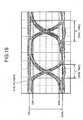
- Fig. 19 illustrates one example of an eye pattern of electric signal waveforms output from a circuit such as the LD driving circuit 200 shown in Fig. 18.
- the LD driving circuit illustrated in this example employs a silicon-germanium semiconductor so as to reduce power consumption of the circuit.
- this LD driving circuit is driven by a negative voltage as shown in Fig. 18, a first transition of an electric signal pulse corresponding to a first transition of an optical signal pulse is a segment of the eye pattern directed downward whereas a second transition thereof is a segment of the eye pattern directed upward. As shown in Fig. 19, a fall time Tf is longer than a rise time Tr by about 40 percents.
- Fig. 20 illustrates one example of an eye pattern of optical signal waveforms (optical output waveforms) output from the LD module shown in Fig. 18 using the LD driving circuit that outputs electric signals having signal waveforms as shown in Fig. 19.
- This example illustrates that optical signal waveforms in various patterns are photoelectrically converted to electric signals and that the electric signals are overlaid through a band filter.
- an upper part is a mark side (light emission) and the horizontal axis indicates time.
- Fig. 20 also illustrates eye mask regions (regions which are an index to determination as to whether a signal is deteriorated and in which the eye pattern should not enter).
- Eye mask prescription indicated by the eye mask regions are an index to the performance of the signal waveform. As a gap (an eye mask margin) between the signal waveform (eye pattern) and the eye mask region is wider, better reception sensitivity characteristics can be attained when an optical receiver receives a signal. In other words, even if an optical signal is lower in power, error occurs less frequently and good transmission characteristics can be ensured.
- the optical output waveform of the LD module is conspicuously deteriorated as shown in Fig. 20.
- Fig. 20 As can be seen from the waveform shown in Fig. 20, there is an enough margin to the eye mask prescription near an upper left part of a central portion of the eye pattern (a rising part indicated by W1 in Fig. 20).
- W1 in Fig. 20 a rising part indicated by W1 in Fig. 20
- the eye mask margin is quite small near an upper right part of the central portion (a rising part indicated by W2 in Fig. 20), with the result there is no margin at all to the eye mask prescription. Therefore, a problem occurs that if, for example, a surrounding temperature rises, a relaxation oscillation frequency of the optical semiconductor falls and the signal waveform cannot satisfy the upper right part of the central portion of the eye mask.
- a cause for this fall of the eye margin is as follows. If the optical semiconductor device is a pulse intensity modulation type optical semiconductor device that modulates a light in a wide band from a low frequency band to a high frequency band, the fall time of the electric signal pulse is late as explained above and the eye mask margin that is a margin of the eye pattern falls due to asymmetry of the electric signal input to the LD module 300. As a result, the transmission characteristics of the optical signal to be output are deteriorated.
- Fig. 21 is a frequency response graph if a signal transmission line P between the LD driving circuit 200 and the LD module 300 shown in Fig. 18 includes a distributed constant circuit such as a micro-strip line and if the LD module 300 is viewed from this distributed constant circuit.
- Fig. 21 demonstrates that a cutoff frequency (a frequency 3 decibels lower from a peak) is about 8.8 gigahertz and that there is a sharp decline of the response characteristics at a frequency near 10 gigahertz. Reasons for the presence of this sharp decline are as follows.
- both ends of inductance elements 311 shown in the example of Fig. 14 are fixed to a ceramic substrate and a plurality of pad sections each including a conductor are provided to arrange wirings by wire bonds. Since each pad section functions as a capacitance, a resonance is generated by these capacitances, a plurality of wires by the wire bonding that connect the LD 310 to pads provided between the inductance element 311 and the matching resistor 309, and a reactance component of the inductance element 311 that constitutes the bias circuit. This results in quite sharp damping characteristics.
- the conventional optical semiconductor device has problems that output characteristics of the optical signal is influenced by poor fall characteristics of the LD driving circuit and the transmission characteristics of the optical signal is thereby deteriorated.
- the conventional optical semiconductor device has a problem that passing characteristics of the LD module suddenly attenuates at the frequency near 10 gigahertz.
- the sharp decline of the characteristics near 10 gigahertz particularly causes the great deterioration of the optical output waveform of the optical semiconductor device. It is significant to solve this problem.
- an object of the present invention to provide an optical semiconductor device which improves the deterioration of an optical output waveform due to the asymmetry between a rise time and a fall time of the output waveform of an LD driving circuit and the deterioration of the optical output waveform such as the deterioration following a sharp decline of passing characteristics of an optical semiconductor module, and which improves the quality of the optical output waveform.
- An optical semiconductor device includes an optical semiconductor element; a first conductor line connected to one electrode of a pair of electrodes of the optical semiconductor device, and supplying an electric signal to the optical semiconductor element; a second conductor line connected to the other electrode of the pair of electrodes of the optical semiconductor element, and supplying an electric signal to the optical semiconductor element; a first inductance element connected to the one electrode of the optical semiconductor element and the first conductor line; and a second inductance element connected to the other electrode of the optical semiconductor element and the second conductor line, wherein the first and the second conductor lines constitute a pair of differential lines.
- the first conductor line and the second conductor line can constitute a pair of differential lines, the first conductor line connected to one electrode of a pair of electrodes which the optical semiconductor device includes can supply an electric signal to the optical semiconductor element, the second conductor line connected to the other electrode of the pair of electrode which the optical semiconductor element includes can supply an electric signal to the optical semiconductor element, the first inductance element connected to the one electrode of the optical semiconductor element and the first conductor line can cut off the electric signal at a high frequency, and the second inductance element connected to the other electrode of the optical semiconductor element and the second conductor line can cut off the electric signal at a high frequency.
- An optical semiconductor device includes an optical semiconductor element; a first differential input terminal supplying an electric signal to one of a pair of electrodes of the optical semiconductor element; a second differential input terminal supplying an electric signal opposite in phase to the electric signal supplied by the first differential input terminal, to the other electrode of the pair of electrodes of the optical semiconductor element; a first inductance element connected to the one electrode of the optical semiconductor element and the first conductor line, and cutting off the electric signal at a high frequency; and a second inductance element connected to the other electrode of the optical semiconductor element and the second conductor line, and cutting off the electric signal at a high frequency.
- An optical semiconductor device includes an optical semiconductor element; a pair of differential amplifiers each having one terminal and the other terminal connected to one electrode and the other electrode of a pair of electrodes of the optical semiconductor element, respectively, and each supplying an electric signal to the optical semiconductor element; a first inductance element connected to the one electrode of the optical semiconductor element, and cutting off the electric signal at a high frequency; and a second inductance element connected to the other electrode of the optical semiconductor element, and cutting off the electric signal at a high frequency.
- a pair of differential amplifiers each having one terminal and the other terminal connected to one electrode and the other electrode of a pair of electrodes which the optical semiconductor element includes, respectively, can supply electric signals to the optical semiconductor element, the first inductance element connected to the one electrode of the optical semiconductor element can cut off the electric signal at a high frequency, and the second inductance element connected to the other electrode of the optical semiconductor element can cut off the electric signal at the high frequency.
- An optical semiconductor device further includes, in addition to the above invention, a pair of matching resistors connected to the one electrode and the other electrode of the optical semiconductor element, respectively, and introducing the electric signals to the optical semiconductor element.
- a pair of resistors connected to the one electrode and the other electrode of the optical semiconductor element, respectively can make impedance matching at the high frequency and efficiently introduce the electric signals to the optical semiconductor element.
- An optical semiconductor device includes, in addition to the above invention, a first bias circuit including the first inductance element and a first resistor connected in parallel to the first inductance element; and a second bias circuit including the second inductance element and a second resistor connected in parallel to the second inductance element.
- An optical semiconductor device includes, in addition to the above invention, a filter that cuts off frequencies higher than at least a maximum repetition frequency of a digital signal, the filter provided between the first and the second conductor lines and the pair of matching resistors.
- the filter provided between the first and the second conductor lines and the pair of matching resistors can cut off frequencies higher than at least the maximum repetition frequency of the digital signal, and remove a ringing of electric input waveforms in unnecessary frequency bands.
- the filter includes a first conductor finger section and a second conductor finger section in which a plurality of conductors crossing the first and the second conductor lines are formed, respectively, to have a comb shape, the first conductor finger section and the second conductor finger sections being alternately arranged.
- the filter which includes the first conductor finger section and the second conductor finger section in which a plurality of conductors crossing the first and the second conductor lines are formed, respectively, to have a comb shape, and in which filter the first conductor finger section and the second conductor finger sections are alternately arranged, can cut off frequencies higher than at least the maximum repetition frequency of the digital signal and remove the ringing of electric input waveforms in unnecessary frequency bands.
- An optical semiconductor device includes, in addition to the above invention, a package containing therein the first and the second conductor lines; a lens that condenses a light emitted from the optical semiconductor element; and an optical fiber holding member that holds an optical fiber.
- a semiconductor optical modulation device including the package containing therein the first and the second conductor lines, the lens that condenses the light emitted from the optical semiconductor element, and the optical fiber holding member that holds the optical fiber can be constituted.
- the first and the second inductance elements are air-cored coils.
- the first and the second air-cored coils enable making the bias circuits for cutting off high frequency electric signals in wide frequency bands small in size.
- the optical semiconductor element is a semiconductor laser diode.
- the semiconductor optical modulation device that reduces the deterioration of the optical output waveforms of the semiconductor laser diode can be constituted.
- the first and the second inductance elements may supply bias currents.
- An optical semiconductor device includes an optical semiconductor element; first and second conductor lines connected to a pair of electrodes of the optical semiconductor element, and supplying differential signals to the optical semiconductor element, respectively; a first terminal electrically connected to the first conductor line and one electrode of the pair of electrodes of the optical semiconductor element; and a second terminal electrically connected to the second conductor line and the other electrode of the optical semiconductor element, wherein the first and the second terminals are connected to bias circuits that cut off high frequencies, respectively.
- the first and the second conductor lines connected to a pair of electrodes of the optical semiconductor element supply differential signals to the optical semiconductor element, respectively, and the first terminal electrically connected to the first conductor line and one electrode of the pair of electrodes of the optical semiconductor element and the second terminal electrically connected to the second conductor line and the other electrode of the optical semiconductor element are connected to the bias circuits that cut off high frequencies, respectively. It is thereby possible to prevent the resonance caused by the reactance components of the inductance elements, the inductances of the wire bonds, and the capacities of the pads, and cut off high frequency electric signals in wide frequency bands.
- An optical semiconductor device includes an optical semiconductor element; a first conductor line having one end connected to one of a pair of electrodes of the optical semiconductor element, and supplying an electric signal to the optical semiconductor element; a second conductor line having one end connected to the other electrode of the pair of electrodes of the optical semiconductor element, and supplying an electric signal to the optical semiconductor element; a first inductance element connected to the one electrode of the optical semiconductor element and the first conductor line; and a second inductance element connected to the other electrode of the optical semiconductor element and the second conductor line, wherein the optical semiconductor element is driven by a push-pull operation.
- the first conductor line connected to one of a pair of electrodes of the optical semiconductor element driven by the push-pull operation can supply an electric signal to the optical semiconductor element
- the second conductor line connected to the other electrode of the pair of electrodes of the optical semiconductor element can supply an electric signal to the optical semiconductor element
- the first inductance element connected to one end of the optical semiconductor element can cut off high frequency electric signals
- the second inductance element connected to the other end of the optical semiconductor element can cut off high frequency electric signals.
- impedances of at least two bias circuits are set asymmetric.
- At least two bias circuits having asymmetric impedances can constitute the semiconductor optical modulation device which improves a waviness of frequency response characteristics.
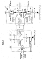
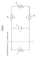
- Fig. 1 is a circuit block diagram which illustrates one example of an optical semiconductor device according to the first embodiment.
- an LD driving circuit 1 includes an input buffer 11 which has a differential input configuration, a pair of differential transistors 12 and 13 which have differential configuration and which output an antiphase signal and a positive phase signal, respectively, a transistor 14 which performs a constant-current operation, and resistors 15 and 16 which are loads of collectors of the differential transistors 12 and 13, respectively, and which make impedance matching.
- the input buffer 11 shapes waveforms of input antiphase signal and positive phase signal, and generates the adjusted antiphase signal and positive phase signal to be input to bases of the differential transistors 12 and 13.
- the paired differential transistors 12 and 13 that have the differential configuration and the transistor 14 constitute a differential amplifier.
- Collector sides of the differential transistors 12 and 13 are connected to one side of the resistors 15 and that of the resistor 16, respectively.
- the other sides of the resistors 15 and 16 are connected to ground terminals, respectively.
- Emitters of the differential transistors 12 and 13 are connected to the transistor 14 which performs the constant-current operation.
- An antiphase signal output terminal of the input buffer 11 is connected to the base of the differential transistor 12, and a positive phase signal output terminal of the input buffer 11 is connected to the base of the differential transistor 13.
- An emitter side of the transistor 14 and a voltage input terminal of the input buffer 11 are both connected to a negative power supply (Vee).
- the differential transistors 12 and 13 may be replaced by field-effect transistors (hereinafter, "FETs"). If the FETs are employed, the anode and cathode of the LD 20 are connected to drains of the FETs, respectively.
- FETs field-effect transistors
- LD module 2 sides of the differential transistors 12 and 13 are connected to the LD 20 having a high frequency impedance of about 5 ohms through the distributed constant circuit 18 and the matching resistors 19a and 19b for impedance matching each having an impedance of about 20 ohms.
- the anode side of the LD 20 is bonded to a conductor line electrically connected to the matching resistor 19b by soldering or the like, and the cathode side of the LD 20 is connected to a conductor line electrically connected to the matching resistor 19a.
- the distributed constant circuit 18 is constituted so that the output terminals of the differential transistors 13 and 12 of differential type in the LD driving circuit 1 are connected to the matching resistors 19a and 19b by differential lines or wire bonds, respectively.
- the differential lines are obtained by arranging two conductor lines to be proximate to each other, and signal transmission is performed so that one of input signals to the two conductor lines is a positive-phase signal and the other input signal is an antiphase signal. It is thereby possible to improve electrical coupling between the two conductor lines and reduce leakage loss of an electric field.
- the conventional single-phase driving type optical semiconductor device since a high current that drives the LD is fed back to the LD driving circuit through a ground, a ground potential changes. This ground potential change often adversely affects an optical reception electronic circuit arranged proximate to the device and detecting a feeble current.
- the optical semiconductor device performs a push-pull operation with respect to the LD using the differential lines. Therefore, the optical semiconductor device in this embodiment has advantages in that the high current carries across the differential lines, the ground potential has less change, and peripheral circuits are less influenced.
- the differential lines include differential type micro-strip lines (micro-strip differential lines) obtained by arranging two signal transmission lines proximate to each other, differential type grounded coplanar lines (grounded coplanar differential lines), differential pins (or leads) obtained by arranging two conductor pins proximate to each other, or the like.
- a solenoid 21 a having a high impedance with respect to a high frequency and a resistor 22a connected in parallel to this solenoid 21 a and reducing a Q value for preventing a resonance constitute a first bias circuit 28a.
- a solenoid 21 b having a high impedance with respect to the high frequency and a resistor 22b connected in parallel to this solenoid 21 b and reducing the Q value for preventing the resonance constitute a second bias circuit 28b.
- Air-cored coils which cause bias currents (direct currents) to pass through, and which suppress modulated signals (electric signals at several hundred kilohertz to several tens of gigahertz) output from the LD driving circuit 1 from leaking from the first and the second bias circuits 28a and 28b, i.e., which cut off high frequency signals are used for the solenoids 21 a and 21 b, respectively.
- the solenoid 21a in the first bias circuit 28a and the solenoid 21 b in the second bias circuit 28b are connected to the conductor lines, one ends of which are electrically connected to the anode and cathode of the LD 20, through the wire bonds 23a and 23b, respectively.
- the bias circuit 28a is connected to the conductor line electrically connected to the matching resistor 19a through the wire bond 23a, and connected to the cathode of the LD 20 through a wire bond 29.
- the bias circuit 28b is connected to the conductor line electrically connected to the matching resistor 19b through the wire bond 23b, and connected to the soldered conductor line (pad) on the anode of the LD 20.
- the anode side of the LD 20 is connected to a ground terminal through the parallel circuit in the second bias circuit 28b.
- the cathode side of the LD 20 is connected to a constant current source 24 through the parallel circuit in the second bias circuit 28a.
- the constant current source 24 includes a transistor and an emitter side of the constant current source 24 is connected to a negative power supply (Vee). This negative power supply is set equal in voltage to the negative power supply (Vee) to which the transistor 14 in the LD driving circuit 1 is connected. Alternatively, they may be set at different voltages.
- DC direct current
- a state of the differential transistor 12 in the LD driving circuit 1 changes from ON to OFF (a state of the differential transistor 13 changes from OFF to ON)
- the modulation current flows in the LD 20 and a state of an laser light output from the LD 20 changes from OFF to ON.
- the state of the differential transistor 13 changes from ON to OFF (the state of the differential transistor 12 changes from OFF to ON)
- the modulation current flowing in the LD 20 decreases and the state of a laser light output of the LD 20 changes from ON to OFF.
- the modulated electrical signals output from the differential transistors 12 and 13 constituted to be differential from each other in the LD driving circuit 1 are transmitted to the LD 20 through the distributed constant circuit 18 and the like, and converted to optical modulation signal in the LD 20.
- the modulated optical signals generated from the LD 20 are condensed on an optical fiber 26 by a condenser lens 25 and the condensed, modulated optical signal is output through this optical fiber 26.
- Fig. 2(a) is an explanatory view which typically illustrates rising and fall characteristics of the paired differential transistors 12 and 13 in the LD driving circuit 1.
- Fig. 2(b) is an explanatory view which illustrates a principle that the rising and fall characteristics of the paired differential transistors 12 and 13 are averaged.
- a rise time of the differential transistor 12 or 13 (it is assumed that the transistors 12 and 13 are equivalent in characteristics) is tr and a fall time thereof is tf, tr and tf satisfies a relationship of tr ⁇ tf. This is already explained above.
- the positive-phase signal and the antiphase signal are passed through the distributed constant circuit 18, and one is connected to the cathode of the LD 20 through the matching resistor 19a and the other is connected to the anode of the LD 20 through the matching resistor 19b.
- the paired transistors perform a differential operation. If the operation is viewed from the LD 310, the operation is simply such that when the differential transistor 203 rises, a current flows in the LD 310, and that when the differential transistor 203 falls, no current flows in the LD 310. Namely, if the operation is viewed from the LD 310 (or the distributed constant circuit that connects the LD driving circuit 200 to the LD 310), the LD 310 is not push-pull driven.
- the circuits in the optical semiconductor device according to the present invention shown in Fig. 1 perform such an push-pull operation. Therefore, the distributed constant circuit 18 serves as differential lines, performs current push and pull for the LD 20 simultaneously. If the operation is viewed from the LD 20, the circuits operate for an average time ((tr + tf) / 2) between the rise time (tr) of the differential transistor 12 and the fall time (tf) of the differential transistor 13. As a result, as shown in Fig. 2(b), the paired transistors 12 and 13 exhibit symmetric rise characteristics that the rise time and the fall time are averaged.
- Fig. 3 illustrates that optical signal waveforms in various patterns are photoelectrically converted to electric signals and that the electric signals are passed through a band filter and overlaid.
- an upper part is a mark side (light emission) and the horizontal axis indicates time.
- waveform asymmetry is improved, there are enough margins to the eye mask prescriptions, and good transmission characteristics can be obtained, as compared with the eye pattern shown in Fig. 20.
- the LD driving circuit 200 is adjusted to have peaking characteristics. If so, a slight ringing at a frequency around 15 gigahertz higher than a signal band often occurs and is superposed on the electric waveform shown in Fig. 19.
- This ringing can lift up the rising waveform of the optical output waveform, a right shoulder (lower right part) of the eye pattern has margins to the eye mask, and the quality of the optical output waveforms can be enhanced.
- a fundamental wave of a digital signal at 10 Gb/s (minimum pulse) is at, for example, 5 gigahertz
- the peaking of the LD driving circuit 200 is adjusted so that the ringing occurs at a harmonics three times higher than 5 gigahertz, i.e., 15 gigahertz, whereby high-quality optical output waveforms can be obtained.
- Japanese Patent Application Laid-Open Publication No. 11-233876 discloses an example of the laser module that transmits data without jitters by holding a balance between differential load impedances.
- the laser module does not perform a push-pull operation if the operation is viewed from the LD. Therefore, the invention disclosed by the publication differs from the present invention.
- Japanese Patent Application Laid-Open Publication No. 5-327617 discloses that only the fall time is improved by reducing the input impedance of the LD which impedance is viewed from the driving circuit. Therefore, the invention of the publication entirely differs in principle from the present invention.
- Fig. 4(a) is a graph which illustrates frequency response characteristics when the LD module 2 shown in Fig. 1 is viewed from the distributed constant circuit 18.
- the bias circuit 23a in which the solenoid 21 a and the resistor 22a are arranged in parallel, is connected to the cathode side of the LD 20 in the LD module 2 shown in Fig. 1
- the bias circuit 23b in which the solenoid 21 b and the resistor 22b are arranged in parallel, is connected to the anode side of the LD 20 in the LD module 2. Therefore, the respective bias circuits 28a and 28b generate a resonance due to the capacitance components of the pad sections provided on the ceramic substrate or the like, similarly to the example of the conventional LD module 300.
- the two bias circuits appear as if they are connected in series. Therefore, an amplitude of the resonance can be reduced, and the sharp decline at the frequency around 10 gigahertz as shown in Fig. 21 is prevented.
- Fig. 4(a) the graph which illustrates the frequency response characteristics when the impedances of the resistors 22a and 22b are set equal is shown.
- Fig. 4(b) is a graph which illustrates the frequency response characteristics when the bias circuits 28a and 28b are set to have different impedances. As shown in Fig. 4(b), waviness is improved as compared with the graph of Fig. 4(a). Specific examples of inductances and resistors will be explained later in the third and the fourth embodiments.
- Japanese Patent Application Laid-Open Publication No. 5-37083 discloses a problem that an inductance Ls of a bonding wire for connecting a bias circuit to a semiconductor laser and a parasitic capacitance Cs1 of a ceramic block of an airtight package provided for connecting the bias circuit to an external circuit cause the deterioration of small signal frequency characteristics.
- metallization applied on a lower surface of a bias line arranged on the ceramic block of the airtight package is removed and the parasitic capacitance in the circuit is thereby removed.
- a lower surface of the ceramic block is a part other than the lower surface of the bias line and metallization thereof is not removed.
- Japanese Patent Application Laid-Open Publication No. 5-37083 employs the single-phase line to supply a modulated signal to the semiconductor laser.
- the publication does not disclose an example of the circuit in which differential lines are employed, an example in which two bias circuits are employed, and an example in which impedances of the two bias circuits are set differently.
- the invention of the publication differs in circuit configuration from the first embodiment of the present invention in which the two bias circuits connected to the differential lines are arranged.
- the invention of Japanese Patent Application Laid-Open Publication No. 5-37083 moves a damping frequency of 3 decibels of the passing characteristics caused by the resonance from 2.5 gigahertz to 2.9 gigahertz on the frequency axis.
- the invention of the publication thus totally differs from the first embodiment of the present invention in which the amplitude of the resonance is changed.
- the optical semiconductor element to which the differential lines are connected is driven by the push-pull operation. Therefore, the first embodiment exhibits advantages in that the asymmetry of the electric driving waveform is improved, the quality of the optical output waveform is improved, and good transmission characteristics can be thereby obtained.
- the bias circuits are arranged on the both sides of the optical semiconductor element to which the differential lines are connected. Therefore, if the optical semiconductor element is assumed as the equivalent circuit, the two bias circuits appear to be connected in series to the optical semiconductor element. Hence, the amplitude of the resonance can be reduced, the sharp decline (ripple) of the passing characteristics followed by the arrangement of the bias circuits can be improved, the quality of the optical output waveform can be improved, and the good transmission characteristics can be thereby obtained.
- the optical semiconductor device in which the LD is directly modulated has been shown.
- the first embodiment is also applicable to an optical semiconductor device separately including a light source that outputs a light of a certain intensity, such as an optical semiconductor device using a field absorption type semiconductor modulation element.
- Such an optical semiconductor device has the same functions and advantages as those of the first embodiment.
- each solenoid is employed as an element that prevents a serial resonance.
- any other element can be used as long as the element has an inductance component (the element is an inductance element).
- the element is an inductance element.
- a chip inductor including a pattern wiring on the ceramic substrate, or a wire having a diameter of 0.01 to 0.5 millimeter and a length of about 10 millimeters may be used.
- the optical semiconductor element to which the differential lines are connected is driven by the push-pull operation. Therefore, the optical semiconductor device has advantages in that the asymmetry of the waveform can be improved, the quality of the optical output waveform is improved, and the good transmission characteristics can be thereby obtained.
- the bias circuits are arranged on the both sides of the optical semiconductor element to which the differential lines are connected. Therefore, the ripple of the passing characteristics followed by the arrangement of the bias circuits can be improved, the quality of the optical output waveform can be improved, and the good transmission characteristics can be thereby obtained.
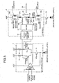
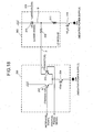
- Fig. 5 is a circuit block diagram which illustrates one example of the optical semiconductor device in the second embodiment.
- the LD driving circuit 1 includes the input buffer 11 which has differential input configuration, the paired differential transistors 12 and 13 which have differential configuration to output an antiphase signal and a positive phase signal, respectively, the transistor 14 which performs a constant-current operation, and the resistors 15 and 16 which are resistors against the loads of collectors of the differential transistors 12 and 13, respectively, and which make impedance matching.
- the input buffer 11 shapes waveforms of input antiphase signal and positive phase signal, and generates the adjusted antiphase signal and positive phase signal to be input to bases of the differential transistors 12 and 13.
- the paired differential transistors 12 and 13 that have the differential configuration and the transistor 14 constitute a differential amplifier.
- Collector sides of the differential transistors 12 and 13 are connected to one side of the resistor 15 and that of the resistor 16, respectively.
- the other sides of the resistors 15 and 16 are connected to ground terminals, respectively.
- Emitters of the differential transistors 12 and 13 are connected to the transistor 14 which performs the constant-current operation.
- the antiphase signal output terminal of the input buffer 11 is connected to the base of the differential transistor 12, and the positive phase signal output terminal of the input buffer 11 is connected to the base of the differential transistor 13.
- An emitter side of the transistor 14 and a voltage input terminal of the input buffer 11 are both connected to the negative power supply (Vee).
- the (collector-side) output terminals of the differential transistors 12 and 13 are connected to the anode and the cathode of the LD 20 through the distributed constant circuit 18, which includes micro-strip lines or grounded coplanar lines, and the matching resistors 19a and 19b, respectively.
- the differential transistors 12 and 13 may be replaced by the FETs. If the FETs are employed, the anode and cathode of the LD 20 are connected to drains of the FETs, respectively.
- the LD module 2 sides of the differential transistors 12 and 13 are connected to the anode side of LD 20 having a high frequency impedance of about 5 ohms by soldering and to the cathode side thereof by the wire bond 29 through the distributed constant circuit 18, a filter 27, and the matching resistors 19a and 19b for impedance matching each having an impedance of about 20 ohms.
- the differential transistors 12 and 13 are connected to the first bias circuit 28a which includes the solenoid 21a having a high impedance with respect to a high frequency and the resistor 22a connected in parallel to this solenoid 21 a and reducing a Q value for preventing a resonance, and to the second bias circuit 28b which includes the solenoid 21b having a high impedance with respect to a high frequency and the resistor 22b connected in parallel to this solenoid 21 b and reducing a Q value for preventing a resonance through wire bonds 23a and 23b, respectively.
- the anode side of the LD 20 is connected to the ground terminal through the wire bond 23b and the parallel circuit in the second bias circuit 28b.
- the cathode side of the LD 20 is connected to the bias constant-current source 24 through the wire bonds 29 and 23a and the parallel circuit in the second bias circuit 28a.
- the constant-current source 24 includes a transistor and an emitter side of the constant current source 24 is connected to the negative voltage source (Vee). This negative voltage source is equal in voltage to the negative voltage source (Vee) to which the transistor 14 in the LD driving circuit 1 is connected. Alternatively, these negative voltage sources may be set at different voltages.
- DC bias currents are supplied to the anode and cathode of the LD 20 through the paired bias circuits 28a and 28b, and high frequency modulated signals are input to the anode and cathode of the LD 20 by the paired differential type differential transistors 12 and 13 in a differential manner.
- a peaking is applied to the LD driving circuit 1 by changing a circuit constant, not shown in Fig. 5, in order to improve the rise characteristics of the differential transistors 12 and 13 in the LD driving circuit 1, a ringing at cycles of about 15 gigahertz occurs.
- the filter 27 shown in Fig. 5 is a lowpass filter for removing this ringing.
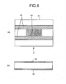
- Fig. 6(a) is a top view of the filter 27, and Fig. 6(b) is an illustration of this filter 27 viewed from an arrow P direction.
- the filter 27 includes a pair of micro-strip differential lines 39 on an upper surface of a ceramic substrate 41 and a ground conductor 40 on a lower surface thereof.
- a comb-like strip conductor electrode 38 is formed alternately from the paired micro-strip conductor lines 39 in an inward direction orthogonal to the micro-strip conductor lines 39.
- Fig. 7 is a graph which compares frequency response characteristics before and after insertion of the filter 27.
- C1 indicates the curve of Fig. 4(b) and indicates a waveform in which the waviness of the response characteristics is improved by setting the impedances of the bias circuits 28a and 28b shown in Fig. 5 asymmetric to each other.
- C2 is a waveform indicating the response characteristics if the peaking is applied to the LD driving circuit 1 shown in Fig. 5 by changing the circuit constant, not shown when a ringing at cycles of about 15 gigahertz occurs.
- C3 is a waveform which indicates the response characteristics when the ringing around 15 gigahertz is cut off by the filter 27.
- Fig. 7 shows that flat and good frequency response characteristics are obtained up to the frequency exceeding 12 gigahertz.
- Japanese Patent Application Laid-Open Publication No. 7-38185 discloses, in Fig. 6, a circuit in which serial circuits including a capacitance and a resistor are inserted in parallel to an LD element and which thereby prevents the ringing of rise characteristics.
- An object of this circuit is, however, to remove an overshoot which occurs because no bias current is applied and a relaxation oscillation, which object differs from the object of the present invention.
- the circuit of the publication differs from the present invention in that the circuit is a single-phase feed type and also differs in circuit configuration.
- Japanese Patent Application Laid-Open Publication No. 7-46194 discloses, in Fig. 1 and Fig. 2, a circuit which changes a matching state by connecting, in parallel, serial circuits including an inductance and a resistor to an LD element between a matching resistor and an LD driving circuit, to thereby prevent a ringing.
- the invention differs from the present invention in object and circuit configuration and also differs in that the circuit is of a single-phase feed type.
- Fig. 8 is a simplified equivalent circuit diagram which simulates a high frequency operation of the optical semiconductor device shown in Fig. 5.
- Reference symbol 31 denotes an output impedance of the LD driving circuit.
- reference symbols 19a and 19b denote the matching resistors
- 20 denotes an LD
- 27 denotes the filter.
- the cutoff frequency fc is approximated to about 10 gigahertz. Since the actual circuit constant is complicated, the cutoff frequency cannot be simply obtained. However, if the capacitance is set based on this cutoff frequency fc, a desired filter effect can be obtained.
- the optical semiconductor device includes the first and the second conductor finger sections in which a plurality of conductors crossing the first and the second conductor lines, respectively, are formed into a comb, the filter in which the first conductor finger section and the second conductor finger section are alternately arranged cuts off frequencies at least higher than a maximum repetition frequency, and the filter removes or reduces the unnecessary ringing of the LD output which occurs when the peaking is applied to the LD driving circuit. Therefore, it is possible to improve a signal-to-noise ratio of the optical output signal, to improve the quality of the optical output waveform, accordingly, and obtain the good transmission characteristics.
- the example of using the comb-like filter as the element that prevents the ringing is shown. Any other element can be used as long as the element has a capacitance component and the element can be constituted by an ordinary conductor pattern or the like.
- the optical semiconductor device in which the LD is directly modulated is illustrated.
- the second embodiment is also applicable to an optical semiconductor device separately including a light source that outputs a light of a certain intensity, such as an optical semiconductor device using a field absorption type semiconductor modulation element.
- Such an optical semiconductor device has the same functions and advantages as those of the second embodiment.
- the advantages of using the differential lines have been explained while centering around the advantage of compensating the asymmetry of the rise/fall characteristics of the LD driving circuit and improving the optical output waveform.
- the differential lines By employing the differential lines, there is an advantage in that frequency characteristics can be improved besides the advantage of compensating the asymmetry of the rise and fall characteristics.
- the advantage of improving the frequency characteristics will be explained while referring to equivalent circuits for specific examples of reactances and resistances.
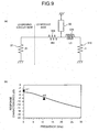
- Fig. 9(a) is a simplified equivalent circuit diagram which simulates a high frequency operation of the conventional optical semiconductor device shown in Fig. 18.
- reference symbol 31 denotes the output impedance of the LD driving circuit
- 309 denotes a matching resistor
- 310 denotes the internal resistance of the LD.
- Reference symbol 329 is the wire bond that connects pads, not shown in Fig. 9(a), provided on the conductor line electrically connected to the matching resistor 309 to the cathode of the LD 310.
- Reference symbol 32 denotes the bias circuit including the inductance element 311 such as the solenoid.
- Fig. 9(b) is a graph which illustrates a simulation result of the frequency response characteristics of this equivalent circuit.
- Fig. 9(b) illustrates the simulation result when the output impedance Z1 of the LD driving circuit side is 50 ohms, the internal resistance r1 of the LD 310 is 8 ohms, the resistance R3 of the matching resistor 309 is 40 ohms, the inductance L of the wire bond 329 is 0.5 nanohenries, and the impedance of the bias circuit 32 is 50 ohms.
- Fig. 9(b) demonstrates that a 3-decibel band (between m1 and m2 where the frequency is lower by 3 decibels than that of m1) is at about 10.6 gigahertz.
- Fig. 10(a) is a simplified equivalent circuit diagram which simulates the high frequency operation of the optical semiconductor device (differential lines) according to the present invention shown in Fig. 1.
- reference symbol 31 denotes the output impedance of the LD driving circuit
- 19a and 19b denote the matching resistors
- 20 denotes the LD
- 29 denotes the wire bond
- 32 and 33 denote the respective bias circuits.
- Fig. 10(b) is a graph which illustrates a simulation result of the frequency response characteristics of this equivalent circuit.
- Fig. 10(b) illustrates the simulation result when the output impedance Z1 of the LD driving circuit side is 100 ohms, the internal resistance r1 of the LD 20 is 8 ohms, the resistances R3 of the matching resistors 19a and 19b are 40 ohms, the inductance L of the wire bond 29 is 0.5 nanohenry, and the impedances of the bias circuits 32 and 33 are 50 ohms.
- Fig. 10(b) demonstrates that a 3-decibel band (between m3 and m4 where the frequency is lower by 3 decibels than that of m3) is at about 18.6 gigahertz.
- the substrate side (anode) of the LD element is fixed to a feed line by soldering or the like. Therefore, the inductance component on the LD module side is mainly caused by the wire bond on the cathode side of the LD element, and there is hardly a difference in impedance component between the differential feed circuit and the singe-phase feed circuit.
- the circuit that employs the differential lines of the impedance viewed from the LD element side is about twice as high as that of the single-phase feed circuit. As a result, by using the differential lines, the frequency characteristics (passing characteristics) are improved.
- the frequency characteristics can be improved.
- Fig. 11(a) is a circuit diagram which illustrates the configuration of the bias circuits in the equivalent circuit shown in Fig. 10(a) in detail. Since the configuration and operation of this equivalent circuit are the same as those explained in the first embodiment, they will not be explained herein. In this fourth embodiment, the characteristics of the equivalent circuit in the first embodiment will be explained while referring to specific examples of inductances, capacitances, and resistances.
- Pieces of data on the respective elements of the equivalent circuit of the optical semiconductor device in the first specific example are as follows if using symbols shown in Fig. 11(a).
- Resistances R1 and R2 of the resistors 22a and 22b are 1,000 ohms
- resistances R3 and R4 of the matching resistors 19a and 19b are 40 ohms
- inductances L1 and L2 of the solenoids 21 a and 21 b are 0.5 nanohenry
- inductances L4 and L5 of the wire bonds 23a and 23b are 3 nanohenries
- the resistance Z1 of the LD driving circuit side is 100 ohms
- the resistance r1 of the LD 20 is 8 ohms
- parasitic capacitances C1, C2, C3, and C4 of the bias circuits are 0.1 picofarad.
- Fig. 11(b) is a graph which illustrates a simulation result of the frequency characteristics based on these circuit conditions.
- Fig. 11(d) is a graph which illustrates a simulation result of the frequency characteristics based on these circuit conditions.
- Fig. 11(b) and Fig. 11(d) As shown in the simulation results of Fig. 11(b) and Fig. 11(d), if the optical semiconductor device employs the differential feed type bias circuits, the amplitude of the resonance ripple caused by the bias circuits can be reduced, as compared with the device that employs the single-phase feed type bias circuits.
- the result of Fig. 11(b) corresponds to that of Fig. 4(a) which illustrates the experimental result of the differential feed type optical semiconductor device in the first embodiment
- Fig. 11(d) corresponds to that of Fig. 21 which illustrates the experimental result of the single-phase feed type optical semiconductor device. It is noted, however, that the experimental results of Fig. 4(a) and Fig. 21 include the frequency characteristics of the LD driving circuits 1 and 200 and a high frequency region is cut off.
- Japanese Patent Application Laid-Open Publication No. 5-37083 discloses the circuit in which a ground surface of a feed-through of the package is removed so as to reduce parasitic capacitances outside of the wall surface of the package of the optical module with a view of improving the resonance ripple which occurs due to the capacitances of the bias circuit.
- This circuit employs a single-phase line and differs in circuit configuration from that of the present invention.
- Fig. 12(a) is a circuit block diagram which illustrates the identical equivalent circuit to that shown in Fig. 11 (a).
- Fig. 12(b) is a graph which illustrates a simulation result based on circuit conditions shown in Fig. 12(a), and corresponds to the graph shown in Fig. 11 (b).
- Fig. 12(c) is a graph which illustrates a simulation result of the frequency response characteristics when the inductance L4 of the wire bond 23a (or 23c) is changed from 3 nanohenries to 1 nanohenry.
- Fig. 13(a) is a circuit block diagram which illustrates the identical equivalent circuit to that shown in Fig. 11 (a).
- Fig. 13(b) is a graph which illustrates a simulation result based on circuit conditions shown in Fig. 13(a), and corresponds to the graph shown in Fig. 11(b).
- Fig. 13(c) is a graph which illustrates a simulation result of the frequency response characteristics when the inductance L1 of the solenoid 21 a is changed in the equivalent circuit of Fig. 11(a).
- the amplitude of the resonance ripple can be reduced.
- the inductance components of the wire bonds connecting the bias circuits to the LD element and the like asymmetric vertically by changing the lengths of the wire bonds and the like, the frequency at which the resonance ripple occurs can be set high.
- the impedances of the inductance element and the resistance connected in parallel to each other in the bias circuit asymmetric vertically, the amplitude of the resonance ripple can be further reduced.
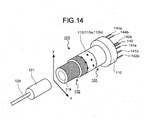
- Fig. 14 illustrates the outside configuration of the optical semiconductor element module (hereinafter, "LD module" since an example of mounting the LD will be mainly explained in this fifth embodiment) 103 which includes a can package 101 and a receptacle 102.
- Fig. 15(a) and Fig. 15(b) are a horizontal sectional view (a view of a surface parallel to x shown in Fig. 14) and a vertical sectional view (a view of a surface parallel to y shown in Fig. 14) of the LD module 103, respectively.
- the can package 101 includes a disk-like stem 110 on which bias feed pins (144a, 144b), high frequency signal pins (141a, 141b), and the like are mounted, a trapezoidal pedestal 111 (a pedestal block) on which a plurality of ceramic substrates are mounted, the condenser lens 25 which condenses a laser light emitted from the LD 20, a cylindrical cap 113 which airtight seals the pedestal 111 and the like from the outside, and the like.
- a disk-like stem 110 on which bias feed pins (144a, 144b), high frequency signal pins (141a, 141b), and the like are mounted
- a trapezoidal pedestal 111 (a pedestal block) on which a plurality of ceramic substrates are mounted
- the condenser lens 25 which condenses a laser light emitted from the LD 20
- a cylindrical cap 113 which airtight seals the pedestal 111 and the like from the outside, and the like.
- the cap 113 has a double cylinder form which includes a first cap member 113a fixed to the stem 110 by projection welding or the like and a second cap member 113b fitted into a tip end side of the first cap member 113a from outward and fixed to the first cap member 113a by YAG welding or the like.
- the first cap member 113a includes stepped outer cylinders, and the outer cylinder having a smaller diameter is provided on the tip end of the outer cylinder having a larger diameter.
- An inner cylinder of the one end-side second cap member 113b is fitted into the outer periphery of the outer cylinder having the smaller diameter, and the first cap member 113a is fixed to the second cap member 113b by through YAG welding.
- a lens insertion hole 114 is formed and the condenser lens 25 is inserted into this hole 114.
- the condenser lens 25 is fixed to the first cap member 113a by a screw, an adhesive material, or the like.
- An internal space 115 of the first cap member 113a is isolated from the outside by a glass window 116, whereby the internal space 115 in which the pedestal 111 is contained is kept airtight. If the internal space 115 can be kept airtight by bonding or soldering the condenser lens 25, the window 116 may be omitted.
- a hole 117 for causing the laser light to pass through is formed in a portion (the other end side) of the second cap member 113b opposite to the condenser lens 25, a hole 117 for causing the laser light to pass through is formed.
- the receptacle 102 includes a ferrule insertion hole 119 for inserting a ferrule 121 (see Fig. 14) to which an optical fiber 120 is connected, and holds the optical fiber 120.
- the dummy ferrule 118 in which an optical fiber 118a is arranged, is press-fitted and fixed into a can package 101-side in the ferrule insertion hole 119.
- One end face of the receptacle 102 on the side, on which the dummy ferrule 118 is fixed, is fixed to an end face on the other end side of the second cap member 113b is fixed to an end face of the other end side of the second cap member 113b in the can package 101 by butt welding using YAG welding or the like.
- the condenser lens 25 is aligned to the dummy ferrule 118 in the receptacle 102 relative to the two directions at right angles with respect to the laser light axis.
- the ferrule 121 to which the optical fiber 120 is connected includes an appropriate mechanism (not shown) for pressing the ferrule 121 toward the dummy ferrule 118 and locking the ferrule 121 to the receptacle 102 when the ferrule 121 is inserted into the ferrule insertion hole 119 of the receptacle 102. Therefore, if the ferrule 121 is inserted into the ferrule insertion hole 119 of the receptacle 102, an end face of the optical fiber 118a in the dummy ferrule 118 abuts on an end face of the optical fiber 120 in the ferrule 121, whereby the fibers are connected (optically coupled) to each other.
- Fig. 16 is a perspective view which illustrates the can package 101 in a state in which the cap 113 is detached.
- the can package 101 includes the disk-like stem 110 on which a plurality of pins are mounted and the trapezoidal pedestal 111 vertically fixed to an inner wall surface of the stem 110 by Ag brazing or the like.
- a pair of high frequency signal pins 141a and 141b to which the differential modulated electric signals (hereinafter, also referred to as “differential high frequency signals”) are transmitted from the LD driving circuit 1, two ground pins 142a and 142b arranged on both sides of these high frequency signal pins 141a and 141b, one monitor signal pin 143 for transmitting a signal of a monitoring light reception element (e.g., a photodiode, (hereinafter, "PD")) 150, a pair of bias feed pins 144a and 144b for supplying bias currents from an external DC bias current source to the LD 20, and a PD chip carrier 145 are mounted.
- a monitoring light reception element e.g., a photodiode, (hereinafter, "PD"
- a current I 1 opposite in phase to the current signal I 2 shown in Fig. 16 is applied to the high frequency signal pin 141b.
- the high frequency signal pins 141a and 141b and the ground pins 142a and 142b constitute a feed-through for causing an electric signal to pass through via the stem 110 while being kept airtight.
- the respective pins are fixed to the stem 110 through dielectrics made of such a material as glass in an airtight sealed state.
- the ground pins 142a and 142b are fixedly attached to an outer wall surface of the stem 110 that constitutes the ground by press-fitting or welding.
- the PD 150 mounted on the PD chip carrier 145 is intended to monitor a monitor light emitted from the LD 20 toward a backward direction.
- Micro-strip differential line substrates 146 and 147, an LD chip carrier 148, and a bias circuit substrate 149 are mounted on an upper surface of the pedestal 111.
- a ground conductor layer that is a plane conductor plate formed on rear surfaces of the micro-strip differential line substrates 146 and 147 and the LD chip carrier 148 to function as the ground is coupled to the upper surface of the pedestal 111 by soldering or the like and electrically connected thereto.
- the pedestal 111 acts as a radiation path for radiating a heat generated from the LD 20 or the like.
- the micro-strip differential line substrate 146 includes a ceramic substrate 151, a pair of strip differential signal lines 152a and 152b formed on an upper surface of the ceramic substrate 151, and the ground conductor layer (not shown) formed on the rear surface of the ceramic substrate 151.
- Pads 153a and 153b to contact with the high frequency signal pins 141a and 141b protruding from the stem 110 are formed on one-end sides of the strip differential signal lines 152a and 152b, respectively.
- Capacitive stubs 154a and 154a for impedance matching which protrude to be closer to each other signal line are formed halfway along the strip differential signal lines 152a and 152b, respectively.
- the strip differential signal lines 152a and 152b are set to have a larger distance therebetween in input-side portions near the stem 110 so as to correct an impedance of the field-through section the impedance of which tends to be low.
- the strip differential signal lines 152a and 152b each include a portion in which the distance between the signal lines is gradually smaller and an output-side portion in which the distance between the signal lines is close and in which the signal lines are arranged in parallel. End portions of the high frequency signal pins 141a and 141b mounted on the stem 110 are connected and fixed to the pads 153a and 153b of the micro-strip differential line substrate 146 by brazing or soldering.
- the micro-strip differential line substrate 147 includes a ceramic substrate 155, a pair of strip differential signal lines 156a and 156b formed on an upper surface of the ceramic substrate 155, and the ground conductor layer (not shown) formed on a rear surface of the ceramic substrate 155.
- Each of the strip differential signal lines 156a and 156b includes a corner curve portion for turning up a signal line direction by about 90 degrees.
- the matching resistors 19a and 19b for impedance matching are formed halfway along the strip differential signal lines 156a and 156b, respectively.
- the strip differential signal lines 152a and 152b are connected to the strip differential signal lines 156a and 156b by wire bonds 157a and 157b, respectively.
- the LD chip carrier 148 includes micro-strip differential lines including a ceramic substrate 158, a pair of strip differential signal lines 159a and 159b formed on an upper surface of the ceramic substrate 158, and the ground conductor layer (not shown) formed on a rear surface of the ceramic substrate 158.
- the LD 20 is mounted on one end of one strip differential signal line 159b on the LD chip carrier 148 so that the anode that is one of the electrodes of the LD 20 directly abuts on one end thereof.
- the cathode that is the other electrode of the LD 20 is connected to one end of the other strip differential signal line 159a by the wire bond 29.
- the strip differential signal lines 156a and 156b are connected to the other ends of the strip differential signal lines 159a and 159b by wire bonds 161a and 161b, respectively.
- the ceramic substrate 158 is made of a material having good thermal conductivity such as aluminum nitride (AIN) or silicon carbide (SiC).
- AIN aluminum nitride
- SiC silicon carbide
- a distributed feedback laser diode element capable of transmitting a modulated signal at 10 Gb/s, for example, is employed.
- Two wiring patterns 162a and 162b and a pair of inductance circuits are formed on the bias circuit (ceramic) substrate 149.
- the solenoid 21a and the resistor 22a that prevents a resonance between an inter-line capacitance of the solenoid 21a and the inductance are arranged to be electrically connected to each other in parallel on the one wiring pattern 162a.
- the solenoids 21a and 21b are arranged to be away from each other so that (extension lines of) central axes of the solenoids 21a and 21b cross each other, preferably are orthogonal to each other to prevent the solenoids 21a and 21b from interfering with each other magnetic field.
- One end portion of the wiring pattern 162a and that of the wiring pattern 162b are connected to the strip line differential signal lines 159a and 159b through wire bonds 23a and 23b, respectively.
- the other end portion of the wiring pattern 162a and that of the wiring pattern 162b are connected to the bias feed pins 144a and 144b provided on the stem 110 through wire bonds 163a and 163b, respectively.
- the characteristic configuration of each section in the can package 101 will be explained in more detail.
- the configuration of the stem 110 will first be explained.
- the differential high frequency signals output from the differential transistors 12 and 13 in the LD driving circuit 1 are input to the can package 101 through a grounded coplanar differential line 170 provided on a substrate arranged outside of the can package 101.
- the grounded coplanar differential line 170 includes a pair of differential signal lines 171a and 171b formed on a substrate, grounds 172a and 172b arranged outside of the differential signal lines 171a and 171b to put the paired differential signal lines 171a and 171b therebetween, and the ground conductor layer (not shown) arranged on a rear surface of the line 170 and connected to the grounds 172a and 172b.
- the differential signal lines 171a and 171b are connected to output terminals 160a and 160b provided on the upper surface of the LD driving circuit 1.
- the output terminal 160a is electrically connected to the collector of the differential transistor 13 whereas the output terminal 160b is electrically connected to the collector of the differential transistor 12.
- the differential signal lines 171a and 171b of the grounded coplanar differential line 170 are connected and fixed to the high frequency signal pins 141a and 141 b provided on the stem 110 by soldering, respectively.
- the grounds 172a and 172b of the grounded coplanar differential line 170 are connected and fixed to the ground pins 142a and 142b provided on the stem 110 by soldering, respectively. Further, since there is a gap between a can package-side end face of the grounded coplanar differential line 170 and the stem 110, the reflection of the high frequency signals due to the lowering of the impedances may be suppressed by filling this gap with a dielectric.
- the stem 110 includes metal such as Kovar (Fe-Ni alloy), soft iron, or CuW (cupper-tungsten), and an upper layer of the stem 110 is normally plated with Ni, gold or the like for soldering.
- a plurality of holes 174, 175, 176a, and 176b are formed to be distributed on the stem 110, and dielectrics 177, 178, 179a, and 179b are inserted into the respective holes 174, 175, 176a, and 176b.
- a pair of pin insertion holes 180a and 180b are formed in the dielectric 177, and the high frequency signal pines 141a and 141b are inserted into and fixed to the pin insertion holes 180a and 180b, respectively.
- holes are formed in the dielectrics 178, 179a, and 179b, and the monitor signal pin 143 and the bias feed pins 144a and 144b are inserted into and fixed to the holes, respectively.
- the dielectric 177 into which the paired high frequency signal pines 141a and 141b are inserted has an oval form in this example. Accordingly, the hole 174 into which the dielectric 177 is inserted has an oval form.
- the other dielectric 178, 179a, and 179b are circular. It is noted that the ground pins 142a and 142b are fixedly attached to an outer wall surface, not shown, of the stem 110 by press-fitting and welding.
- Lengths of portions of the two high frequency signal pins 141a and 141b which protrude toward at least one outside of the dielectric 177 are set smaller than those of the monitor signal pin 143 and the bias feed pins 144a and 144b in light of high frequency characteristics.
- the signal transmitted over the high frequency signal pins 141a and 141b can be promptly transferred to the strip differential signal lines 152a and 152b on the micro-strip differential line substrate 146 when the signals are out of the dielectric 177. Since the monitor signal pins 143 and the bias feed pins 144a and 144b have no strict restrictions for the high frequency characteristics, the protruding lengths are secured to some extent, thereby facilitating wire bond connection operation and the like.
- Kovar glass for example, is preferably used or borosilicate glass may be used.
- metal such as Kovar or 50-percent Ni-Fe alloy is used.
- the grounded coplanar differential line 170, the high frequency signal pins 141 a and 141 b, the ground pins 142a and 142b, the wire bonds 157a and 157b, and the micro-strip differential line substrates 146 and 147 constitute the distributed constant circuit 18.
- the paths among them are all constituted by the differential lines to drive the LD 20.
- the pins penetrating the stem 110 by penetrating the paired high frequency signal pins 141a and 141b through the oval dielectric 177, they act as the differential pins constituting the differential lines.
- the ground potential changes. This ground potential change often adversely affects the optical reception electronic circuit arranged proximate to the device and detecting the feeble current.
- the optical semiconductor device performs the push-pull operation with respect to the LD 20 using the differential lines. Therefore, the optical semiconductor device in this embodiment has advantages in that the high current is carried across the differential lines, the ground potential has less change, and peripheral circuits are less influenced.
- the pin exposure region on the LD driving circuit 1-side is constituted to have the differential lines and the ground pins 142a and 142b are arranged outside of the region, to thereby set the impedance of this section lower than that in the conventional optical semiconductor device. Therefore, the difference in impedance between this section and the feed-through section is small, as compared with the conventional art and discontinuity of the electric field is reduced, and the passing characteristics and reflection characteristics can be thereby improved.
- the glass is used as the dielectric 177 arranged around the high frequency signal pins 141a and 141b. Therefore, in the inner section of the stem (the feed-through section in which the high frequency signal pins 141a and 141b are surrounded by the dielectric 177, hereinafter, also referred to as "unexposed region"), if the high frequency signal pins 141a and 141b each having a diameter of about 3.5 millimeters to 6 millimeters at which the pins can be handled easily are provided, and the holes of arbitrary shapes are formed in the stem 110 having a diameter of about 3.5 millimeters to 6 millimeters, then the impedance of the inner section tends to be extremely lowered.
- a cross-sectional area of the dielectric 177 arranged around the high frequency pins may be set large. If so, however, the optical semiconductor device cannot satisfy requirements for microfabrication and space saving.
- the protruding lengths of the two high frequency signal pins 141a and 141b toward the LD 20 are set small so that they can be promptly transferred to the strip differential signal lines 152a and 152b on the micro-strip differential line substrate 146 when the signals are out of the dielectric 177.
- the distance between the strip differential signal lines 152a and 152b on the micro-strip differential line substrate 146 in the portions which are connected to the high frequency signal pins 141a and 141b, respectively and which are closer to the stem 110 are set larger than the distance therebetween in, for example, the portions closer to the micro-strip line substrate 147, or set slightly larger than the distance between the high frequency signal pins 141a and 141b.
- the distance between the lines in the differential line portions right after the lines are out of the stem 110 is set large to thereby purposely create the high impedance portion.
- the impedance is cancelled by this high impedance portion and the low impedance portion inside of the stem (in the pin unexposed region), whereby impedance matching is made as a whole.
- the pin unexposed region feed-through section
- the impedance matching is made in the overall device by slightly generating a high impedance after the region.
- the paired stubs 154a and 154b for impedance matching are formed halfway along the strip differential signal lines 152a and 152b, respectively.
- the impedance is reduced by the paired stubs 154a and 154b, thereby preventing occurrence of mismatching between the strip differential signal lines 152a and 152b and the strip differential lines 156a and 156b, respectively.
- the reactance components in the driver-side pin exposed region and those in the pin unexposed region (feed-through section) are compensated for each other, and the passing characteristics and the reflection characteristics are thereby improved.
- the paired stubs 154a and 154b protrude not outward but inward (so as to be closer to each other signal line), which, therefore, contributes to microfabrication of the micro-strip differential line substrate 146. If it is unnecessary to make the micro-strip differential line substrate 146 small in size, the stubs 154a and 154b may protrude outward of the differential lines 152a and 151b.
- the differential line substrates for connecting the high frequency signal pins 141a and 141b to the LD 20, the bias circuit substrate for supplying the DC bias currents to the LD 20, and the monitor PD 50.
- the micro-strip differential line substrates 146 and 147 and the bias circuit substrate 149 are arranged on the both sides of the LD chip carrier 148 to put the LD chip carrier 148 therebetween.
- the strip differential signal lines 152a and 152b on the micro-strip differential line substrate 146 and the strip differential signal lines 156a and 156b on the micro-strip differential line substrate 147, the wiring patterns 162a and 162b including a pair of inductance circuits, and the LD 20 are arranged generally in a U-shaped fashion.
- micro-strip differential line substrates 146 and 147 are provided at the positions shifted sideways from the LD chip carrier 148.
- the transparent dielectric 177 for sealing and fixing the high frequency signal pins 141a and 141b is provided at the position shifted sideways from the LD chip carrier 148.
- the LD chip carrier 148 on which the LD 20 serving as the heat source is mounted is separated from the other substrates and provided as an independent substrate. Thanks to this, it suffices to use the ceramic substrate material, such as the aluminum nitride substrate (AIN), which is expensive and which has good radiation characteristics only for the LD chip carrier 148 and to use the ceramic substrate material, such as inexpensive Al 2 O 3 for the other substrates (the micro-strip differential line substrates 146 and 147, and the bias circuit substrate 149). Thus, cost reduction can be realized.
- the ceramic substrate material such as the aluminum nitride substrate (AIN)
- the micro-strip differential line substrate 146 for impedance matching and the micro-strip differential line substrate 147 for arranging the matching resistors 19a and 19b are provided as separate substrates. Therefore, it is possible to cut out the ceramic substrates economically, thereby contributing to cost reduction.
- the parallel circuit connected to the bias feed pins 144a and 144b and including the solenoid 21a and the resistor 22a and the parallel circuit including the solenoid 21b and the resistor 22b are arranged on the bias circuit substrate 149, thereby reducing the area of the bias circuit substrate. This can, therefore, contribute to cost reduction and microfabrication.
- a thickness of the dielectric 177 is set smaller than a depth of the hole 174 formed in the stem 110, i.e., a width of the stem 110, and a hole 195 having an LD-side opening portion formed conically is formed in the stem 110.
- the grounded coplanar differential line may be employed in place of the micro-strip differential line substrates 146 and 147.
- the grounded coplanar differential line includes the paired differential signal line formed on the substrate, the grounds arranged outside of the differential signal lines so as to put the paired differential signal lines therebetween, and the ground conductor layer arranged on the rear surface of the substrate.
- Fig. 17(a) is a top view of the optical semiconductor element module in a state in which an upper cap 401 is detached
- Fig. 17(b) is a cross-sectional view taken along II of Fig. 17(a) (note, however, that Fig. 17(b) is in a state in which the upper cap 401 is attached).
- the LD 20 mounted on the can package 101 explained in the previous embodiment, various constituent elements including a substrate 501 on which the LD 20 is mounted, and the LD driving circuit 1 are contained in a box-like (butterfly-like) optical semiconductor package 402.
- the positive-phase and antiphase differential signals are input to the input buffer 11 of the LD driving circuit 1 as already explained.
- the dielectric 177 feed-through
- the differential signals are transmitted through differential lines 178a and 178b provided on the dielectric 177 while keeping an interior and an exterior of the package airtight.
- One end of the differential line 178a and that of the differential line 178b are soldered to the high frequency signal pins 141a and 141b, respectively, outside of the optical semiconductor package 402.
- the high frequency signal pins 141a and 141b are arranged proximate to each other until positions at which the pins 141a and 141b are put between the ground pins 142a and 142b connected to the ground, and constitute the differential lines.
- the other ends of the differential lines 178a and 178b are connected to one ends of differential strip lines 411 provided on a substrate 502, respectively.
- the other ends of the differential strip lines 411 are connected to one ends of differential strip lines provided on a substrate 503.
- the other ends of the differential strip lines provided on the substrate 503 are connected to differential signal input terminals of the LD driving circuit 1 through wire bonds, respectively, and electrically connected to the input buffer 11 in the LD driving circuit 1.
- the output terminals of the LD driving circuit 1 electrically connected to the differential transistors 12 and 13, are connected to one ends of the differential lines provided on a substrate 504 through wire bonds, respectively.
- the other ends of the differential lines provided on the substrate 504 are connected to one ends of differential lines provided on the substrate 501 through wire bonds, respectively.
- the anode of the LD 20 is soldered to the other end side of one of the differential lines on the substrate 501 as shown in Fig. 5.
- the other end side of the other differential line on the substrate 501 is connected to the cathode of the LD 20 through the wire bond as shown in Fig. 5.
- the matching resistors 19a and 19b are provided on the one end side of the substrate 501. As shown in Fig.
- the bias circuit 28a in which the solenoid 21a and the resistor 22a are connected in parallel and the bias circuit 28b in which the solenoid 21 b and the resistor 22b are connected in parallel are provided on the substrate 505.
- the bias circuits 28a and 28b are connected to the differential lines on the substrate 501, respectively. Further, the bias circuits 28a and 28b are connected to conductor lines on a ceramic substrate 450 through wire bonds, respectively.
- the bias circuits 28a and 28b are connected to respective conductor leads 451 through wire bonds and the ceramic substrate 450 (feed-through).
- the ceramic substrate 450 is fitted into the sidewall of the package, and transmits the bias currents and control signals for the LD driving circuit 1 inside and outside of the optical semiconductor package 402 while keeping airtight.
- the LD driving circuit 1, and the substrates 501, 503, 504, and 505 are mounted on a metallic conductor mount 510.
- a lens 520 which includes a lens and a holder that holds the lens is coupled to a side surface of the metallic conductor mount 510.
- the lens 520 is arranged to condense a light on the optical fiber 120 through the other optical components.
- the upper cap 401 is welded to an upper surface of the optical semiconductor package 402, and a window glass 600 is coupled to a light pass-through hole in a front sidewall of the optical semiconductor package 402, thereby securing airtightness.
- the optical fiber 120 is held by an optical fiber holding section 403.
- the differential signals are input to the LD driving circuit 1 using the high frequency signal pins 141a and 141b constituting the differential lines, the differential strip lines 411, and the other differential lines. Therefore, similarly to the preceding embodiments, it is possible to suppress the deterioration of the high frequency characteristics and improve airtightness.
- the optical semiconductor element to which the differential lines are connected is driven by the push-pull operation. Therefore, the optical semiconductor device has advantages in that the asymmetry of the waveform can be improved, the quality of the optical output waveform can be improved, and that the good transmission characteristics can be thereby obtained.
- the bias circuits are arranged on the both electrode sides of the optical semiconductor element to which the differential lines are connected, respectively. Therefore, the optical semiconductor device has advantages in that the ripple of the passing characteristics following the bias circuits can be improved, the quality of the optical output waveform can be improved, and that the good transmission characteristics can be thereby obtained.
- the present invention as the optical semiconductor element having good transmission characteristics or as the optical semiconductor device that includes the optical semiconductor element, is suited to high speed optical communications.
Abstract
Description
- The present invention relates to an optical semiconductor device including an optical semiconductor element that outputs an optical signal modulated based on an electric signal.
- Fig. 18 is a circuit diagram which illustrates one example of a conventional single-phase feed type optical semiconductor device. Circuits similar to such a circuit are disclosed by, for example, Japanese Patent Application Laid-Open Publication Nos. 9-200150 and 8-172401.
- In the optical semiconductor device shown in Fig. 18, an
LD driving circuit 200 that drives a semiconductor laser diode element 310 (hereinafter, "LD") is connected to anLD module 300. A light emission output of the LD 310 is output from anoptical fiber 316.Differential transistors transistor 204, are applied with complementary data input signals (a positive phase signal and an antiphase signal), respectively, and output a positive-phase signal. A collector of thedifferential transistor 202 is grounded. A collector of thedifferential transistor 203 is connected to one end of adamping resistor 309, and the other end of thedamping resistor 309 is connected to one electrode (cathode) of theLD 310. The cathode of the LD 310 is connected to one end of aninductance element 311 having a high impedance with respect to a high frequency, such as a chip inductance. The other end of theinductance element 311 is connected to a constantcurrent source 314 that supplies a bias current to theLD 310. Theinductance element 311 constitutes a bias circuit for theLD module 300. - Fig. 19 illustrates one example of an eye pattern of electric signal waveforms output from a circuit such as the
LD driving circuit 200 shown in Fig. 18. The LD driving circuit illustrated in this example employs a silicon-germanium semiconductor so as to reduce power consumption of the circuit. - If this LD driving circuit is driven by a negative voltage as shown in Fig. 18, a first transition of an electric signal pulse corresponding to a first transition of an optical signal pulse is a segment of the eye pattern directed downward whereas a second transition thereof is a segment of the eye pattern directed upward. As shown in Fig. 19, a fall time Tf is longer than a rise time Tr by about 40 percents.
- Fig. 20 illustrates one example of an eye pattern of optical signal waveforms (optical output waveforms) output from the LD module shown in Fig. 18 using the LD driving circuit that outputs electric signals having signal waveforms as shown in Fig. 19. This example illustrates that optical signal waveforms in various patterns are photoelectrically converted to electric signals and that the electric signals are overlaid through a band filter. In Fig. 20, an upper part is a mark side (light emission) and the horizontal axis indicates time. Fig. 20 also illustrates eye mask regions (regions which are an index to determination as to whether a signal is deteriorated and in which the eye pattern should not enter).
- Eye mask prescription indicated by the eye mask regions are an index to the performance of the signal waveform. As a gap (an eye mask margin) between the signal waveform (eye pattern) and the eye mask region is wider, better reception sensitivity characteristics can be attained when an optical receiver receives a signal. In other words, even if an optical signal is lower in power, error occurs less frequently and good transmission characteristics can be ensured.
- That is, in order to obtain a signal at a low error rate when the optical signal output from the optical semiconductor device is received and converted to an electric signal and the electric signal is reproduced, it is necessary to prevent the eye pattern from entering the eye mask regions.
- Nevertheless, if a modulated signal at 10 Gb/s or more is to be transmitted, the optical output waveform of the LD module is conspicuously deteriorated as shown in Fig. 20. As can be seen from the waveform shown in Fig. 20, there is an enough margin to the eye mask prescription near an upper left part of a central portion of the eye pattern (a rising part indicated by W1 in Fig. 20). However, the eye mask margin is quite small near an upper right part of the central portion (a rising part indicated by W2 in Fig. 20), with the result there is no margin at all to the eye mask prescription. Therefore, a problem occurs that if, for example, a surrounding temperature rises, a relaxation oscillation frequency of the optical semiconductor falls and the signal waveform cannot satisfy the upper right part of the central portion of the eye mask.
- As can be seen, in the conventional optical semiconductor shown in Fig. 18, the margin to the eye mask prescription falls as shown in Fig. 20.
- A cause for this fall of the eye margin is as follows. If the optical semiconductor device is a pulse intensity modulation type optical semiconductor device that modulates a light in a wide band from a low frequency band to a high frequency band, the fall time of the electric signal pulse is late as explained above and the eye mask margin that is a margin of the eye pattern falls due to asymmetry of the electric signal input to the
LD module 300. As a result, the transmission characteristics of the optical signal to be output are deteriorated. - Fig. 21 is a frequency response graph if a signal transmission line P between the
LD driving circuit 200 and theLD module 300 shown in Fig. 18 includes a distributed constant circuit such as a micro-strip line and if theLD module 300 is viewed from this distributed constant circuit. Fig. 21 demonstrates that a cutoff frequency (afrequency 3 decibels lower from a peak) is about 8.8 gigahertz and that there is a sharp decline of the response characteristics at a frequency near 10 gigahertz. Reasons for the presence of this sharp decline are as follows. - In a high frequency region such as a region at the frequency near 10 gigahertz, both ends of
inductance elements 311 shown in the example of Fig. 14 are fixed to a ceramic substrate and a plurality of pad sections each including a conductor are provided to arrange wirings by wire bonds. Since each pad section functions as a capacitance, a resonance is generated by these capacitances, a plurality of wires by the wire bonding that connect theLD 310 to pads provided between theinductance element 311 and thematching resistor 309, and a reactance component of theinductance element 311 that constitutes the bias circuit. This results in quite sharp damping characteristics. - As can be seen, the conventional optical semiconductor device has problems that output characteristics of the optical signal is influenced by poor fall characteristics of the LD driving circuit and the transmission characteristics of the optical signal is thereby deteriorated.
- Further, the conventional optical semiconductor device has a problem that passing characteristics of the LD module suddenly attenuates at the frequency near 10 gigahertz. The sharp decline of the characteristics near 10 gigahertz particularly causes the great deterioration of the optical output waveform of the optical semiconductor device. It is significant to solve this problem.
- It is, therefore, an object of the present invention to provide an optical semiconductor device which improves the deterioration of an optical output waveform due to the asymmetry between a rise time and a fall time of the output waveform of an LD driving circuit and the deterioration of the optical output waveform such as the deterioration following a sharp decline of passing characteristics of an optical semiconductor module, and which improves the quality of the optical output waveform.
- An optical semiconductor device according to the present invention includes an optical semiconductor element; a first conductor line connected to one electrode of a pair of electrodes of the optical semiconductor device, and supplying an electric signal to the optical semiconductor element; a second conductor line connected to the other electrode of the pair of electrodes of the optical semiconductor element, and supplying an electric signal to the optical semiconductor element; a first inductance element connected to the one electrode of the optical semiconductor element and the first conductor line; and a second inductance element connected to the other electrode of the optical semiconductor element and the second conductor line, wherein the first and the second conductor lines constitute a pair of differential lines.
- According to the present invention, the first conductor line and the second conductor line can constitute a pair of differential lines, the first conductor line connected to one electrode of a pair of electrodes which the optical semiconductor device includes can supply an electric signal to the optical semiconductor element, the second conductor line connected to the other electrode of the pair of electrode which the optical semiconductor element includes can supply an electric signal to the optical semiconductor element, the first inductance element connected to the one electrode of the optical semiconductor element and the first conductor line can cut off the electric signal at a high frequency, and the second inductance element connected to the other electrode of the optical semiconductor element and the second conductor line can cut off the electric signal at a high frequency.
- An optical semiconductor device according to next invention includes an optical semiconductor element; a first differential input terminal supplying an electric signal to one of a pair of electrodes of the optical semiconductor element; a second differential input terminal supplying an electric signal opposite in phase to the electric signal supplied by the first differential input terminal, to the other electrode of the pair of electrodes of the optical semiconductor element; a first inductance element connected to the one electrode of the optical semiconductor element and the first conductor line, and cutting off the electric signal at a high frequency; and a second inductance element connected to the other electrode of the optical semiconductor element and the second conductor line, and cutting off the electric signal at a high frequency.
- According to the present invention, the first differential input terminal connected to one of the pair of electrodes which the optical semiconductor includes can supply an electric signal to the optical semiconductor element, the second differential input terminal connected to the other electrode of the pair of electrodes which the optical semiconductor includes can supply an electric signal to the optical semiconductor element, the first inductance element connected to the one electrode of the optical semiconductor element can cut off the electric signal at a high frequency, and the second inductance element connected to the other electrode of the optical semiconductor element can cut off the electric signal at the high frequency.
- An optical semiconductor device according to next invention includes an optical semiconductor element; a pair of differential amplifiers each having one terminal and the other terminal connected to one electrode and the other electrode of a pair of electrodes of the optical semiconductor element, respectively, and each supplying an electric signal to the optical semiconductor element; a first inductance element connected to the one electrode of the optical semiconductor element, and cutting off the electric signal at a high frequency; and a second inductance element connected to the other electrode of the optical semiconductor element, and cutting off the electric signal at a high frequency.
- According to the present invention, a pair of differential amplifiers each having one terminal and the other terminal connected to one electrode and the other electrode of a pair of electrodes which the optical semiconductor element includes, respectively, can supply electric signals to the optical semiconductor element, the first inductance element connected to the one electrode of the optical semiconductor element can cut off the electric signal at a high frequency, and the second inductance element connected to the other electrode of the optical semiconductor element can cut off the electric signal at the high frequency.
- An optical semiconductor device according to next invention further includes, in addition to the above invention, a pair of matching resistors connected to the one electrode and the other electrode of the optical semiconductor element, respectively, and introducing the electric signals to the optical semiconductor element.
- According to the present invention, a pair of resistors connected to the one electrode and the other electrode of the optical semiconductor element, respectively, can make impedance matching at the high frequency and efficiently introduce the electric signals to the optical semiconductor element.
- An optical semiconductor device according to next invention includes, in addition to the above invention, a first bias circuit including the first inductance element and a first resistor connected in parallel to the first inductance element; and a second bias circuit including the second inductance element and a second resistor connected in parallel to the second inductance element.
- According to the present invention, the first bias circuit including the first inductance element and the first resistor connected in parallel to the first inductance element and the second bias circuit including the second inductance element and the second resistor connected in parallel to the second inductance element can prevent a resonance caused by reactance components of the inductance elements, inductances of wire bonds, capacities of pads, and parasitic capacitances of the inductance elements, and cut off electric signals at high frequencies in wide frequency bands.
- An optical semiconductor device according to next invention includes, in addition to the above invention, a filter that cuts off frequencies higher than at least a maximum repetition frequency of a digital signal, the filter provided between the first and the second conductor lines and the pair of matching resistors.
- According to the present invention, the filter provided between the first and the second conductor lines and the pair of matching resistors can cut off frequencies higher than at least the maximum repetition frequency of the digital signal, and remove a ringing of electric input waveforms in unnecessary frequency bands.
- In an optical semiconductor device according to next invention, the filter includes a first conductor finger section and a second conductor finger section in which a plurality of conductors crossing the first and the second conductor lines are formed, respectively, to have a comb shape, the first conductor finger section and the second conductor finger sections being alternately arranged.
- According to the present invention, the filter which includes the first conductor finger section and the second conductor finger section in which a plurality of conductors crossing the first and the second conductor lines are formed, respectively, to have a comb shape, and in which filter the first conductor finger section and the second conductor finger sections are alternately arranged, can cut off frequencies higher than at least the maximum repetition frequency of the digital signal and remove the ringing of electric input waveforms in unnecessary frequency bands.
- An optical semiconductor device according to next invention includes, in addition to the above invention, a package containing therein the first and the second conductor lines; a lens that condenses a light emitted from the optical semiconductor element; and an optical fiber holding member that holds an optical fiber.
- According to the present invention, a semiconductor optical modulation device including the package containing therein the first and the second conductor lines, the lens that condenses the light emitted from the optical semiconductor element, and the optical fiber holding member that holds the optical fiber can be constituted.
- In an optical semiconductor device according to next invention, the first and the second inductance elements are air-cored coils.
- According to the present invention, the first and the second air-cored coils enable making the bias circuits for cutting off high frequency electric signals in wide frequency bands small in size.
- In an optical semiconductor device according to next invention, the optical semiconductor element is a semiconductor laser diode.
- According to the present invention, the semiconductor optical modulation device that reduces the deterioration of the optical output waveforms of the semiconductor laser diode can be constituted.
- The first and the second inductance elements may supply bias currents.
- An optical semiconductor device according to next invention includes an optical semiconductor element; first and second conductor lines connected to a pair of electrodes of the optical semiconductor element, and supplying differential signals to the optical semiconductor element, respectively; a first terminal electrically connected to the first conductor line and one electrode of the pair of electrodes of the optical semiconductor element; and a second terminal electrically connected to the second conductor line and the other electrode of the optical semiconductor element, wherein the first and the second terminals are connected to bias circuits that cut off high frequencies, respectively.
- According to the present invention, the first and the second conductor lines connected to a pair of electrodes of the optical semiconductor element supply differential signals to the optical semiconductor element, respectively, and the first terminal electrically connected to the first conductor line and one electrode of the pair of electrodes of the optical semiconductor element and the second terminal electrically connected to the second conductor line and the other electrode of the optical semiconductor element are connected to the bias circuits that cut off high frequencies, respectively. It is thereby possible to prevent the resonance caused by the reactance components of the inductance elements, the inductances of the wire bonds, and the capacities of the pads, and cut off high frequency electric signals in wide frequency bands.
- An optical semiconductor device according to next invention includes an optical semiconductor element; a first conductor line having one end connected to one of a pair of electrodes of the optical semiconductor element, and supplying an electric signal to the optical semiconductor element; a second conductor line having one end connected to the other electrode of the pair of electrodes of the optical semiconductor element, and supplying an electric signal to the optical semiconductor element; a first inductance element connected to the one electrode of the optical semiconductor element and the first conductor line; and a second inductance element connected to the other electrode of the optical semiconductor element and the second conductor line, wherein the optical semiconductor element is driven by a push-pull operation.
- According to the present invention, the first conductor line connected to one of a pair of electrodes of the optical semiconductor element driven by the push-pull operation can supply an electric signal to the optical semiconductor element, the second conductor line connected to the other electrode of the pair of electrodes of the optical semiconductor element can supply an electric signal to the optical semiconductor element, the first inductance element connected to one end of the optical semiconductor element can cut off high frequency electric signals, and the second inductance element connected to the other end of the optical semiconductor element can cut off high frequency electric signals.
- In an optical semiconductor device according to next invention, impedances of at least two bias circuits are set asymmetric.
- According to the present invention, at least two bias circuits having asymmetric impedances can constitute the semiconductor optical modulation device which improves a waviness of frequency response characteristics.
-
- Fig. 1 is a circuit block diagram which illustrates one example of an optical semiconductor device according to the first embodiment; Fig. 2(a) is an explanatory view which typically illustrate rise characteristics and fall characteristics of a pair of differential transistors in an LD driving circuit; Fig. 2(b) is an explanatory view which illustrates a principle that the rise characteristics and the fall characteristics of the pair of differential transistors are averaged; Fig. 3 illustrates that optical signal waveforms in various patterns are photoelectrically converted to electric signals, the electric signals are passed through a band filter, and that the electric signals are overlaid; Fig. 4(a) is a graph which illustrates frequency response characteristics when the LD module shown in Fig. 1 is viewed from a distributed constant circuit; Fig. 4(b) is a graph which illustrates frequency response characteristics when respective bias circuits are set to have different impedances; Fig. 5 is a circuit block diagram which illustrates one example of the optical semiconductor device according to the second embodiment; Fig. 6(a) is a top view of a filter; Fig. 6(b) is an illustration of this filter viewed from an arrow P direction; Fig. 7 is a graph which compares frequency characteristics before and after the filter is inserted; Fig. 8 is an equivalent circuit diagram which simulates a high frequency operation of the optical semiconductor device shown in Fig. 5; Fig. 9(a) is a simplified equivalent circuit diagram which simulates a high frequency operation of a conventional semiconductor device shown in Fig. 18; Fig. 9(b) is a graph which illustrates a simulation result of the frequency response characteristics of this equivalent circuit; Fig. 10(a) is a simplified equivalent circuit diagram which simulates the high frequency operation of the optical semiconductor device (differential lines) according to the present invention shown in Fig. 1; Fig. 10(b) is a graph which illustrates a simulation result of the frequency response characteristics of this equivalent circuit; Fig. 11 (a) is a circuit block diagram which illustrates the configuration of a bias circuit in the equivalent circuit shown in Fig. 10(a) in detail; Fig. 11 (b) is a graph which illustrates the simulation result of the frequency response characteristics based on circuit conditions shown in Fig. 11 (a); Fig. 11 (c) is a circuit block diagram which illustrates the configuration of the bias circuit in the equivalent circuit shown in Fig. 9(a) in detail; Fig. 11 (d) is a graph which illustrates the simulation result of the frequency response characteristics based on the circuit conditions; Fig. 12(a) is a circuit block diagram which illustrates an identical equivalent circuit to that shown in Fig. 11 (a); Fig. 12(b) is a graph which illustrates the simulation result based on circuit conditions shown in Fig. 12(a); Fig. 12(c) is a graph which illustrates the simulation result of frequency response characteristics in the equivalent circuit shown in Fig. 11 (a) when an inductance L4 of a wire bond 23a (or 23b) is changed from 3 nanohenries to 1 nanohenry; Fig. 13(a) illustrates an identical equivalent circuit to that shown in Fig. 11(a); Fig. 13(b) is a graph which illustrates a simulation result based on circuit conditions shown in Fig. 13(a); Fig. 13(c) is a graph which illustrates the simulation result of the frequency response characteristics when an inductance L1 of an inductance element is changed in the equivalent circuit shown in Fig. 11 (a); Fig. 14 illustrates the outside configuration of the LD module which includes a can package and a receptacle; Fig. 15(a) is a horizontal sectional view (a view of a surface parallel to x shown in Fig. 14) of the LD module; Fig. 15(b) is a vertical sectional view (a view of a surface parallel to y shown in Fig. 14) of the LD module; Fig. 16 is a perspective view which illustrates the can package in a state in which a cap is detached; Fig. 17(a) is a top view in a state in which an upper cap is detached; Fig. 17(b) is a cross-sectional view taken along a line II of Fig. 17(a) in a state in which the upper cap is attached; Fig. 18 is a circuit diagram which illustrates one example of a conventional single-phase feed type optical semiconductor device; Fig. 19 illustrates one example of an eye pattern of electric signal waveforms output from a circuit such as an LD driving circuit shown in Fig. 18; Fig. 20 illustrates one example of an eye pattern of optical signal waveforms (optical output waveforms) output from the LD module shown in Fig. 18; and Fig. 21 is a graph which illustrates the frequency response characteristics when a signal transmission path P between the LD driving circuit and the LD module shown in Fig. 18 is constituted by a distributed constant circuit such as a micro-strip line and when the LD module is viewed from this distributed constant circuit.
-
- Exemplary embodiments of the optical semiconductor device according to the present invention is described in detail below with reference to the accompanying drawings.
- Fig. 1 is a circuit block diagram which illustrates one example of an optical semiconductor device according to the first embodiment. In Fig. 1, an
LD driving circuit 1 includes an input buffer 11 which has a differential input configuration, a pair ofdifferential transistors transistor 14 which performs a constant-current operation, andresistors differential transistors - The input buffer 11 shapes waveforms of input antiphase signal and positive phase signal, and generates the adjusted antiphase signal and positive phase signal to be input to bases of the
differential transistors - The paired
differential transistors transistor 14 constitute a differential amplifier. Collector sides of thedifferential transistors resistors 15 and that of theresistor 16, respectively. The other sides of theresistors differential transistors transistor 14 which performs the constant-current operation. An antiphase signal output terminal of the input buffer 11 is connected to the base of thedifferential transistor 12, and a positive phase signal output terminal of the input buffer 11 is connected to the base of thedifferential transistor 13. An emitter side of thetransistor 14 and a voltage input terminal of the input buffer 11 are both connected to a negative power supply (Vee). - Collector-side output terminals of the
differential transistors LD 20 through a distributedconstant circuit 18, which includes micro-strip lines or grounded coplanar lines, and matchingresistors - The
differential transistors LD 20 are connected to drains of the FETs, respectively. -
LD module 2 sides of thedifferential transistors LD 20 having a high frequency impedance of about 5 ohms through the distributedconstant circuit 18 and thematching resistors LD 20 is bonded to a conductor line electrically connected to the matchingresistor 19b by soldering or the like, and the cathode side of theLD 20 is connected to a conductor line electrically connected to the matchingresistor 19a. The distributedconstant circuit 18 is constituted so that the output terminals of thedifferential transistors LD driving circuit 1 are connected to thematching resistors - In, for example, the conventional single-phase driving type optical semiconductor device, since a high current that drives the LD is fed back to the LD driving circuit through a ground, a ground potential changes. This ground potential change often adversely affects an optical reception electronic circuit arranged proximate to the device and detecting a feeble current. In this embodiment, by contrast, the optical semiconductor device performs a push-pull operation with respect to the LD using the differential lines. Therefore, the optical semiconductor device in this embodiment has advantages in that the high current carries across the differential lines, the ground potential has less change, and peripheral circuits are less influenced.
- The differential lines include differential type micro-strip lines (micro-strip differential lines) obtained by arranging two signal transmission lines proximate to each other, differential type grounded coplanar lines (grounded coplanar differential lines), differential pins (or leads) obtained by arranging two conductor pins proximate to each other, or the like.
- A
solenoid 21 a having a high impedance with respect to a high frequency and aresistor 22a connected in parallel to thissolenoid 21 a and reducing a Q value for preventing a resonance constitute afirst bias circuit 28a. Asolenoid 21 b having a high impedance with respect to the high frequency and aresistor 22b connected in parallel to thissolenoid 21 b and reducing the Q value for preventing the resonance constitute asecond bias circuit 28b. Air-cored coils which cause bias currents (direct currents) to pass through, and which suppress modulated signals (electric signals at several hundred kilohertz to several tens of gigahertz) output from theLD driving circuit 1 from leaking from the first and thesecond bias circuits solenoids solenoid 21a in thefirst bias circuit 28a and thesolenoid 21 b in thesecond bias circuit 28b are connected to the conductor lines, one ends of which are electrically connected to the anode and cathode of theLD 20, through thewire bonds bias circuit 28a is connected to the conductor line electrically connected to the matchingresistor 19a through thewire bond 23a, and connected to the cathode of theLD 20 through awire bond 29. Thebias circuit 28b is connected to the conductor line electrically connected to the matchingresistor 19b through thewire bond 23b, and connected to the soldered conductor line (pad) on the anode of theLD 20. - The anode side of the
LD 20 is connected to a ground terminal through the parallel circuit in thesecond bias circuit 28b. The cathode side of theLD 20 is connected to a constantcurrent source 24 through the parallel circuit in thesecond bias circuit 28a. The constantcurrent source 24 includes a transistor and an emitter side of the constantcurrent source 24 is connected to a negative power supply (Vee). This negative power supply is set equal in voltage to the negative power supply (Vee) to which thetransistor 14 in theLD driving circuit 1 is connected. Alternatively, they may be set at different voltages. - The
bias circuits wire bonds - With the driving configuration of this
LD 20, direct current (hereinafter, "DC") bias currents are supplied to the anode and cathode of theLD 20 through the paired first andsecond bias circuits LD 20 in a differential manner by the paireddifferential transistors - Namely, if a state of the
differential transistor 12 in theLD driving circuit 1 changes from ON to OFF (a state of thedifferential transistor 13 changes from OFF to ON), the modulation current flows in theLD 20 and a state of an laser light output from theLD 20 changes from OFF to ON. If the state of thedifferential transistor 13 changes from ON to OFF (the state of thedifferential transistor 12 changes from OFF to ON), the modulation current flowing in theLD 20 decreases and the state of a laser light output of theLD 20 changes from ON to OFF. - Accordingly, the modulated electrical signals output from the
differential transistors LD driving circuit 1 are transmitted to theLD 20 through the distributedconstant circuit 18 and the like, and converted to optical modulation signal in theLD 20. The modulated optical signals generated from theLD 20 are condensed on anoptical fiber 26 by acondenser lens 25 and the condensed, modulated optical signal is output through thisoptical fiber 26. - Fig. 2(a) is an explanatory view which typically illustrates rising and fall characteristics of the paired
differential transistors LD driving circuit 1. Fig. 2(b) is an explanatory view which illustrates a principle that the rising and fall characteristics of the paireddifferential transistors - As shown in Fig. 2(a), if a rise time of the
differential transistor 12 or 13 (it is assumed that thetransistors - Further, as explained, the positive-phase signal and the antiphase signal are passed through the distributed
constant circuit 18, and one is connected to the cathode of theLD 20 through the matchingresistor 19a and the other is connected to the anode of theLD 20 through the matchingresistor 19b. By so connecting, when thedifferential transistor 12 rises, thedifferential transistor 13 simultaneously rises and when thedifferential transistor 12 falls, thedifferential transistor 13 simultaneously falls. Therefore, if the operation is viewed from theLD 20, theLD 20 is push-pull driven by the paireddifferential transistors - As for the circuits in the conventional optical semiconductor device shown in Fig. 18, in the
LD driving circuit 200, the paired transistors perform a differential operation. If the operation is viewed from theLD 310, the operation is simply such that when thedifferential transistor 203 rises, a current flows in theLD 310, and that when thedifferential transistor 203 falls, no current flows in theLD 310. Namely, if the operation is viewed from the LD 310 (or the distributed constant circuit that connects theLD driving circuit 200 to the LD 310), theLD 310 is not push-pull driven. - The circuits in the optical semiconductor device according to the present invention shown in Fig. 1 perform such an push-pull operation. Therefore, the distributed
constant circuit 18 serves as differential lines, performs current push and pull for theLD 20 simultaneously. If the operation is viewed from theLD 20, the circuits operate for an average time ((tr + tf) / 2) between the rise time (tr) of thedifferential transistor 12 and the fall time (tf) of thedifferential transistor 13. As a result, as shown in Fig. 2(b), the pairedtransistors - Fig. 3 illustrates that optical signal waveforms in various patterns are photoelectrically converted to electric signals and that the electric signals are passed through a band filter and overlaid. In Fig. 3, an upper part is a mark side (light emission) and the horizontal axis indicates time. As can be seen from Fig. 3, waveform asymmetry is improved, there are enough margins to the eye mask prescriptions, and good transmission characteristics can be obtained, as compared with the eye pattern shown in Fig. 20.
- Near an upper right part (a rising part indicated by F in Fig: 3) of a central portion of the eye pattern, in particular, there is an enough margin to the eye mask prescription, so that a margin to a waveform deterioration following a lowering in the relaxation oscillation frequency of the
LD 20 due to an increase of a using temperature. - Further, in order to the rise characteristics of the LD driving circuit having the relatively long rise time and fall time shown in Fig. 19, the
LD driving circuit 200 is adjusted to have peaking characteristics. If so, a slight ringing at a frequency around 15 gigahertz higher than a signal band often occurs and is superposed on the electric waveform shown in Fig. 19. - This ringing can lift up the rising waveform of the optical output waveform, a right shoulder (lower right part) of the eye pattern has margins to the eye mask, and the quality of the optical output waveforms can be enhanced. If a fundamental wave of a digital signal at 10 Gb/s (minimum pulse) is at, for example, 5 gigahertz, the peaking of the
LD driving circuit 200 is adjusted so that the ringing occurs at a harmonics three times higher than 5 gigahertz, i.e., 15 gigahertz, whereby high-quality optical output waveforms can be obtained. - Japanese Patent Application Laid-Open Publication No. 11-233876 discloses an example of the laser module that transmits data without jitters by holding a balance between differential load impedances. However, the laser module does not perform a push-pull operation if the operation is viewed from the LD. Therefore, the invention disclosed by the publication differs from the present invention.
- Japanese Patent Application Laid-Open Publication No. 5-327617 discloses that only the fall time is improved by reducing the input impedance of the LD which impedance is viewed from the driving circuit. Therefore, the invention of the publication entirely differs in principle from the present invention.
- Fig. 4(a) is a graph which illustrates frequency response characteristics when the
LD module 2 shown in Fig. 1 is viewed from the distributedconstant circuit 18. As explained, thebias circuit 23a, in which thesolenoid 21 a and theresistor 22a are arranged in parallel, is connected to the cathode side of theLD 20 in theLD module 2 shown in Fig. 1, and thebias circuit 23b, in which thesolenoid 21 b and theresistor 22b are arranged in parallel, is connected to the anode side of theLD 20 in theLD module 2. Therefore, therespective bias circuits conventional LD module 300. However, if theLD module 2 is viewed as an equivalent circuit from the distributedconstant circuit 18 side, the two bias circuits appear as if they are connected in series. Therefore, an amplitude of the resonance can be reduced, and the sharp decline at the frequency around 10 gigahertz as shown in Fig. 21 is prevented. In the example shown in Fig. 4(a), the graph which illustrates the frequency response characteristics when the impedances of theresistors - Fig. 4(b) is a graph which illustrates the frequency response characteristics when the
bias circuits - Japanese Patent Application Laid-Open Publication No. 5-37083 discloses a problem that an inductance Ls of a bonding wire for connecting a bias circuit to a semiconductor laser and a parasitic capacitance Cs1 of a ceramic block of an airtight package provided for connecting the bias circuit to an external circuit cause the deterioration of small signal frequency characteristics. According to the publication, with a view of reducing the influence of this parasitic capacitance Cs1, metallization applied on a lower surface of a bias line arranged on the ceramic block of the airtight package is removed and the parasitic capacitance in the circuit is thereby removed. A lower surface of the ceramic block is a part other than the lower surface of the bias line and metallization thereof is not removed.
- Nevertheless, the invention disclosed by Japanese Patent Application Laid-Open Publication No. 5-37083 employs the single-phase line to supply a modulated signal to the semiconductor laser. The publication does not disclose an example of the circuit in which differential lines are employed, an example in which two bias circuits are employed, and an example in which impedances of the two bias circuits are set differently. In addition, the invention of the publication differs in circuit configuration from the first embodiment of the present invention in which the two bias circuits connected to the differential lines are arranged.
- Moreover, the invention of Japanese Patent Application Laid-Open Publication No. 5-37083 moves a damping frequency of 3 decibels of the passing characteristics caused by the resonance from 2.5 gigahertz to 2.9 gigahertz on the frequency axis. The invention of the publication thus totally differs from the first embodiment of the present invention in which the amplitude of the resonance is changed.
- As can be seen, according to the first embodiment, the optical semiconductor element to which the differential lines are connected is driven by the push-pull operation. Therefore, the first embodiment exhibits advantages in that the asymmetry of the electric driving waveform is improved, the quality of the optical output waveform is improved, and good transmission characteristics can be thereby obtained.
- Further, the bias circuits are arranged on the both sides of the optical semiconductor element to which the differential lines are connected. Therefore, if the optical semiconductor element is assumed as the equivalent circuit, the two bias circuits appear to be connected in series to the optical semiconductor element. Hence, the amplitude of the resonance can be reduced, the sharp decline (ripple) of the passing characteristics followed by the arrangement of the bias circuits can be improved, the quality of the optical output waveform can be improved, and the good transmission characteristics can be thereby obtained.
- In the first embodiment, the optical semiconductor device in which the LD is directly modulated has been shown. The first embodiment is also applicable to an optical semiconductor device separately including a light source that outputs a light of a certain intensity, such as an optical semiconductor device using a field absorption type semiconductor modulation element. Such an optical semiconductor device has the same functions and advantages as those of the first embodiment.
- In the first embodiment, each solenoid is employed as an element that prevents a serial resonance. However, any other element can be used as long as the element has an inductance component (the element is an inductance element). For example, a chip inductor including a pattern wiring on the ceramic substrate, or a wire having a diameter of 0.01 to 0.5 millimeter and a length of about 10 millimeters may be used.
- As explained so far, according to the optical semiconductor device in the first embodiment, the optical semiconductor element to which the differential lines are connected is driven by the push-pull operation. Therefore, the optical semiconductor device has advantages in that the asymmetry of the waveform can be improved, the quality of the optical output waveform is improved, and the good transmission characteristics can be thereby obtained.
- Further, according to the optical semiconductor device in the first embodiment, the bias circuits are arranged on the both sides of the optical semiconductor element to which the differential lines are connected. Therefore, the ripple of the passing characteristics followed by the arrangement of the bias circuits can be improved, the quality of the optical output waveform can be improved, and the good transmission characteristics can be thereby obtained.
- Fig. 5 is a circuit block diagram which illustrates one example of the optical semiconductor device in the second embodiment. In Fig. 5, the
LD driving circuit 1 includes the input buffer 11 which has differential input configuration, the paireddifferential transistors transistor 14 which performs a constant-current operation, and theresistors differential transistors - The input buffer 11 shapes waveforms of input antiphase signal and positive phase signal, and generates the adjusted antiphase signal and positive phase signal to be input to bases of the
differential transistors - The paired
differential transistors transistor 14 constitute a differential amplifier. Collector sides of thedifferential transistors resistor 15 and that of theresistor 16, respectively. The other sides of theresistors differential transistors transistor 14 which performs the constant-current operation. The antiphase signal output terminal of the input buffer 11 is connected to the base of thedifferential transistor 12, and the positive phase signal output terminal of the input buffer 11 is connected to the base of thedifferential transistor 13. An emitter side of thetransistor 14 and a voltage input terminal of the input buffer 11 are both connected to the negative power supply (Vee). - The (collector-side) output terminals of the
differential transistors LD 20 through the distributedconstant circuit 18, which includes micro-strip lines or grounded coplanar lines, and thematching resistors - The
differential transistors LD 20 are connected to drains of the FETs, respectively. - The
LD module 2 sides of thedifferential transistors LD 20 having a high frequency impedance of about 5 ohms by soldering and to the cathode side thereof by thewire bond 29 through the distributedconstant circuit 18, afilter 27, and thematching resistors differential transistors first bias circuit 28a which includes thesolenoid 21a having a high impedance with respect to a high frequency and theresistor 22a connected in parallel to thissolenoid 21 a and reducing a Q value for preventing a resonance, and to thesecond bias circuit 28b which includes thesolenoid 21b having a high impedance with respect to a high frequency and theresistor 22b connected in parallel to thissolenoid 21 b and reducing a Q value for preventing a resonance throughwire bonds - The anode side of the
LD 20 is connected to the ground terminal through thewire bond 23b and the parallel circuit in thesecond bias circuit 28b. The cathode side of theLD 20 is connected to the bias constant-current source 24 through thewire bonds second bias circuit 28a. The constant-current source 24 includes a transistor and an emitter side of the constantcurrent source 24 is connected to the negative voltage source (Vee). This negative voltage source is equal in voltage to the negative voltage source (Vee) to which thetransistor 14 in theLD driving circuit 1 is connected. Alternatively, these negative voltage sources may be set at different voltages. - Similarly to the first embodiment, DC bias currents are supplied to the anode and cathode of the
LD 20 through the pairedbias circuits LD 20 by the paired differential typedifferential transistors - If a peaking is applied to the
LD driving circuit 1 by changing a circuit constant, not shown in Fig. 5, in order to improve the rise characteristics of thedifferential transistors LD driving circuit 1, a ringing at cycles of about 15 gigahertz occurs. Thefilter 27 shown in Fig. 5 is a lowpass filter for removing this ringing. - In a 1.31 micrometer wavelength band in which optical fiber dispersion is less influential, waveform change after optical fiber transmission is small and this ringing waveform is attenuated by a filter of a receiver. Therefore, an optical output waveform having larger margins to the eye mask can be obtained. This ringing can be, therefore, actively utilized for the improvement of the signal waveform after the signal is passed through the filter of the receiver. However, in a 1.55 micrometer wavelength band in which the optical fiber dispersion influence is large, if this ringing waveform is present, a wavelength chirp resulting from the optical semiconductor light emitting element grows and the chirp may possibly adversely affect the waveform after the signal is transmitted over the optical fiber. For this reason, the ringing is removed by the
filter 27. - Fig. 6(a) is a top view of the
filter 27, and Fig. 6(b) is an illustration of thisfilter 27 viewed from an arrow P direction. In Fig. 6(a) and Fig. 6(b), thefilter 27 includes a pair of micro-stripdifferential lines 39 on an upper surface of aceramic substrate 41 and aground conductor 40 on a lower surface thereof. In addition, a comb-likestrip conductor electrode 38 is formed alternately from the pairedmicro-strip conductor lines 39 in an inward direction orthogonal to the micro-strip conductor lines 39. - Fig. 7 is a graph which compares frequency response characteristics before and after insertion of the
filter 27. In Fig. 7, C1 indicates the curve of Fig. 4(b) and indicates a waveform in which the waviness of the response characteristics is improved by setting the impedances of thebias circuits LD driving circuit 1 shown in Fig. 5 by changing the circuit constant, not shown when a ringing at cycles of about 15 gigahertz occurs. C3 is a waveform which indicates the response characteristics when the ringing around 15 gigahertz is cut off by thefilter 27. Fig. 7 shows that flat and good frequency response characteristics are obtained up to the frequency exceeding 12 gigahertz. - Japanese Patent Application Laid-Open Publication No. 7-38185 discloses, in Fig. 6, a circuit in which serial circuits including a capacitance and a resistor are inserted in parallel to an LD element and which thereby prevents the ringing of rise characteristics. An object of this circuit is, however, to remove an overshoot which occurs because no bias current is applied and a relaxation oscillation, which object differs from the object of the present invention. Further, the circuit of the publication differs from the present invention in that the circuit is a single-phase feed type and also differs in circuit configuration.
- Japanese Patent Application Laid-Open Publication No. 7-46194 discloses, in Fig. 1 and Fig. 2, a circuit which changes a matching state by connecting, in parallel, serial circuits including an inductance and a resistor to an LD element between a matching resistor and an LD driving circuit, to thereby prevent a ringing. However, the invention differs from the present invention in object and circuit configuration and also differs in that the circuit is of a single-phase feed type.
- Fig. 8 is a simplified equivalent circuit diagram which simulates a high frequency operation of the optical semiconductor device shown in Fig. 5.
Reference symbol 31 denotes an output impedance of the LD driving circuit. On an LD module side, reference symbols correspond to those that denote the respective element of the LD module shown in Fig. 5, i.e.,reference symbols - If it is assumed herein that resistances of the
matching resistors LD 20 is r, a capacitance of thefilter 27 is C, and the output impedance of the LD driving circuit is Z, then an approximate equation of a cutoff frequency fc of this equivalent circuit is expressed as follows:Z - For example, if the impedance Z of the LD driving circuit side is 100 ohms, the internal resistance r of the
LD 20 is 8 ohms, and the resistances Rd of the matching resistors are 45 ohms, and the capacitance C of thefilter 27 is 0.16 picofarad, then the cutoff frequency fc is approximated to about 10 gigahertz. Since the actual circuit constant is complicated, the cutoff frequency cannot be simply obtained. However, if the capacitance is set based on this cutoff frequency fc, a desired filter effect can be obtained. - As explained, according to the second embodiment, the optical semiconductor device includes the first and the second conductor finger sections in which a plurality of conductors crossing the first and the second conductor lines, respectively, are formed into a comb, the filter in which the first conductor finger section and the second conductor finger section are alternately arranged cuts off frequencies at least higher than a maximum repetition frequency, and the filter removes or reduces the unnecessary ringing of the LD output which occurs when the peaking is applied to the LD driving circuit. Therefore, it is possible to improve a signal-to-noise ratio of the optical output signal, to improve the quality of the optical output waveform, accordingly, and obtain the good transmission characteristics.
- In the second embodiment, the example of using the comb-like filter as the element that prevents the ringing is shown. Any other element can be used as long as the element has a capacitance component and the element can be constituted by an ordinary conductor pattern or the like.
- In the second embodiment, the optical semiconductor device in which the LD is directly modulated is illustrated. The second embodiment is also applicable to an optical semiconductor device separately including a light source that outputs a light of a certain intensity, such as an optical semiconductor device using a field absorption type semiconductor modulation element. Such an optical semiconductor device has the same functions and advantages as those of the second embodiment.
- In the first embodiment, the advantages of using the differential lines have been explained while centering around the advantage of compensating the asymmetry of the rise/fall characteristics of the LD driving circuit and improving the optical output waveform. By employing the differential lines, there is an advantage in that frequency characteristics can be improved besides the advantage of compensating the asymmetry of the rise and fall characteristics. In this embodiment, the advantage of improving the frequency characteristics will be explained while referring to equivalent circuits for specific examples of reactances and resistances.
- Fig. 9(a) is a simplified equivalent circuit diagram which simulates a high frequency operation of the conventional optical semiconductor device shown in Fig. 18. In Fig. 9(a),
reference symbol 31 denotes the output impedance of the LD driving circuit, 309 denotes a matching resistor, and 310 denotes the internal resistance of the LD.Reference symbol 329 is the wire bond that connects pads, not shown in Fig. 9(a), provided on the conductor line electrically connected to the matchingresistor 309 to the cathode of theLD 310.Reference symbol 32 denotes the bias circuit including theinductance element 311 such as the solenoid. Although the resistances should actually be reactances, the resistances are shown for simplifying explanation of fundamental passing characteristics in Fig. 9 and Fig. 10. - Fig. 9(b) is a graph which illustrates a simulation result of the frequency response characteristics of this equivalent circuit. Fig. 9(b) illustrates the simulation result when the output impedance Z1 of the LD driving circuit side is 50 ohms, the internal resistance r1 of the
LD 310 is 8 ohms, the resistance R3 of the matchingresistor 309 is 40 ohms, the inductance L of thewire bond 329 is 0.5 nanohenries, and the impedance of thebias circuit 32 is 50 ohms. Fig. 9(b) demonstrates that a 3-decibel band (between m1 and m2 where the frequency is lower by 3 decibels than that of m1) is at about 10.6 gigahertz. - Fig. 10(a) is a simplified equivalent circuit diagram which simulates the high frequency operation of the optical semiconductor device (differential lines) according to the present invention shown in Fig. 1. In Fig. 10(a),
reference symbol 31 denotes the output impedance of the LD driving circuit, 19a and 19b denote the matching resistors, 20 denotes the LD, 29 denotes the wire bond, and 32 and 33 denote the respective bias circuits. - Fig. 10(b) is a graph which illustrates a simulation result of the frequency response characteristics of this equivalent circuit. Fig. 10(b) illustrates the simulation result when the output impedance Z1 of the LD driving circuit side is 100 ohms, the internal resistance r1 of the
LD 20 is 8 ohms, the resistances R3 of thematching resistors wire bond 29 is 0.5 nanohenry, and the impedances of thebias circuits - The substrate side (anode) of the LD element is fixed to a feed line by soldering or the like. Therefore, the inductance component on the LD module side is mainly caused by the wire bond on the cathode side of the LD element, and there is hardly a difference in impedance component between the differential feed circuit and the singe-phase feed circuit. On the other hand, the circuit that employs the differential lines of the impedance viewed from the LD element side is about twice as high as that of the single-phase feed circuit. As a result, by using the differential lines, the frequency characteristics (passing characteristics) are improved.
- As can be understood, by connecting the LD driving circuit to the LD module using the differential lines, the frequency characteristics can be improved.
- Fig. 11(a) is a circuit diagram which illustrates the configuration of the bias circuits in the equivalent circuit shown in Fig. 10(a) in detail. Since the configuration and operation of this equivalent circuit are the same as those explained in the first embodiment, they will not be explained herein. In this fourth embodiment, the characteristics of the equivalent circuit in the first embodiment will be explained while referring to specific examples of inductances, capacitances, and resistances.
- Pieces of data on the respective elements of the equivalent circuit of the optical semiconductor device in the first specific example are as follows if using symbols shown in Fig. 11(a). Resistances R1 and R2 of the
resistors matching resistors solenoids wire bonds LD 20 is 8 ohms, and parasitic capacitances C1, C2, C3, and C4 of the bias circuits are 0.1 picofarad. Fig. 11(b) is a graph which illustrates a simulation result of the frequency characteristics based on these circuit conditions. - Fig. 11(c) is a circuit block diagram which illustrates the configuration of the bias circuits in the equivalent circuit shown in Fig. 9(a) in detail. Since the configuration and operation of this equivalent circuit are the same as those explained in the conventional art, they will not be explained herein. Pieces of data on the respective elements of the equivalent circuit are as follows if using symbols shown in Fig. 11(c). R2 is 1,000 ohms, R3 is 40 ohms, the inductance L2 of the
inductance element 311 is 100 nanohenries, L3 = 0.5 nanohenry, L5 = 3 nanohenries, and the parasitic capacitances C2 and C4 of the bias circuits are 0.1 picofarad. Fig. 11(d) is a graph which illustrates a simulation result of the frequency characteristics based on these circuit conditions. - As shown in the simulation results of Fig. 11(b) and Fig. 11(d), if the optical semiconductor device employs the differential feed type bias circuits, the amplitude of the resonance ripple caused by the bias circuits can be reduced, as compared with the device that employs the single-phase feed type bias circuits. The result of Fig. 11(b) corresponds to that of Fig. 4(a) which illustrates the experimental result of the differential feed type optical semiconductor device in the first embodiment, and that of Fig. 11(d) corresponds to that of Fig. 21 which illustrates the experimental result of the single-phase feed type optical semiconductor device. It is noted, however, that the experimental results of Fig. 4(a) and Fig. 21 include the frequency characteristics of the
LD driving circuits - Japanese Patent Application Laid-Open Publication No. 5-37083 discloses the circuit in which a ground surface of a feed-through of the package is removed so as to reduce parasitic capacitances outside of the wall surface of the package of the optical module with a view of improving the resonance ripple which occurs due to the capacitances of the bias circuit. This circuit, however, employs a single-phase line and differs in circuit configuration from that of the present invention.
- The characteristics of the bias circuits if different conditions are set for the equivalent circuit of the optical semiconductor device in the first embodiment, will be explained as the second specific example of the inductances, capacitances, and resistances.
- Fig. 12(a) is a circuit block diagram which illustrates the identical equivalent circuit to that shown in Fig. 11 (a). Fig. 12(b) is a graph which illustrates a simulation result based on circuit conditions shown in Fig. 12(a), and corresponds to the graph shown in Fig. 11 (b). Fig. 12(c) is a graph which illustrates a simulation result of the frequency response characteristics when the inductance L4 of the
wire bond 23a (or 23c) is changed from 3 nanohenries to 1 nanohenry. - As shown in the simulation results of Fig. 12(b) and Fig. 12(c), by making the inductance components of the wire bond connecting the bias circuit to the LD element and the like asymmetric vertically, a frequency at which the resonance ripple occurs can be set high. Although the amplitude of the ripple increases, a region in which the ripple occurs can be forced out of the band. Therefore, this is advantageous when a desired band is to be secured.
- The characteristics of the bias circuits if different conditions are set for the equivalent circuit of the optical semiconductor device in the first embodiment, will be explained as the third specific example of inductances, capacitances, and resistances.
- Fig. 13(a) is a circuit block diagram which illustrates the identical equivalent circuit to that shown in Fig. 11 (a). Fig. 13(b) is a graph which illustrates a simulation result based on circuit conditions shown in Fig. 13(a), and corresponds to the graph shown in Fig. 11(b). Fig. 13(c) is a graph which illustrates a simulation result of the frequency response characteristics when the inductance L1 of the
solenoid 21 a is changed in the equivalent circuit of Fig. 11(a). As regards thesolenoid 21 a and theresistance 22a, Fig. 13(b) is the graph before the inductance L1 is changed while setting L1 = 100 nanohenries and R1 = 1,000 ohms, and Fig. 13(c) is the graph after the inductance L1 is changed while setting L1 = 10 nanohenries and R1 = 400 ohms. - As shown in the simulation results of Fig. 13(b) and Fig. 13(c), by making the impedances of the
solenoid 21a (or 21b) and theresistor 22a (or 22b) connected in parallel to each other in the bias circuit asymmetric vertically, the amplitude of the resonance ripple can be further reduced. This is the same in content as that shown in the experimental result of Fig. 4(b) which illustrates the first embodiment. In the experimental result of Fig. 4(b) which illustrates the first embodiment, the frequency characteristics of theLD driving circuit 1 are included and the high frequency region is cut off. - As can be seen, according to the fourth embodiment, by connecting the LD driving circuit to the LD module using the differential lines, the amplitude of the resonance ripple can be reduced. In addition, by making the inductance components of the wire bonds connecting the bias circuits to the LD element and the like asymmetric vertically by changing the lengths of the wire bonds and the like, the frequency at which the resonance ripple occurs can be set high. Further, by making the impedances of the inductance element and the resistance connected in parallel to each other in the bias circuit asymmetric vertically, the amplitude of the resonance ripple can be further reduced.
- An optical semiconductor element module in the fifth embodiment of the present invention will first be explained with reference to Fig. 14 to Fig. 16.
- Fig. 14 illustrates the outside configuration of the optical semiconductor element module (hereinafter, "LD module" since an example of mounting the LD will be mainly explained in this fifth embodiment) 103 which includes a can package 101 and a
receptacle 102. Fig. 15(a) and Fig. 15(b) are a horizontal sectional view (a view of a surface parallel to x shown in Fig. 14) and a vertical sectional view (a view of a surface parallel to y shown in Fig. 14) of theLD module 103, respectively. - As shown in Fig. 14 and Fig. 15, the can package 101 includes a disk-
like stem 110 on which bias feed pins (144a, 144b), high frequency signal pins (141a, 141b), and the like are mounted, a trapezoidal pedestal 111 (a pedestal block) on which a plurality of ceramic substrates are mounted, thecondenser lens 25 which condenses a laser light emitted from theLD 20, acylindrical cap 113 which airtight seals thepedestal 111 and the like from the outside, and the like. - As shown in Fig. 15, the
cap 113 has a double cylinder form which includes afirst cap member 113a fixed to thestem 110 by projection welding or the like and asecond cap member 113b fitted into a tip end side of thefirst cap member 113a from outward and fixed to thefirst cap member 113a by YAG welding or the like. Specifically, thefirst cap member 113a includes stepped outer cylinders, and the outer cylinder having a smaller diameter is provided on the tip end of the outer cylinder having a larger diameter. An inner cylinder of the one end-sidesecond cap member 113b is fitted into the outer periphery of the outer cylinder having the smaller diameter, and thefirst cap member 113a is fixed to thesecond cap member 113b by through YAG welding. - On the tip end side of the
first cap member 113a, alens insertion hole 114 is formed and thecondenser lens 25 is inserted into thishole 114. Thecondenser lens 25 is fixed to thefirst cap member 113a by a screw, an adhesive material, or the like. Aninternal space 115 of thefirst cap member 113a is isolated from the outside by aglass window 116, whereby theinternal space 115 in which thepedestal 111 is contained is kept airtight. If theinternal space 115 can be kept airtight by bonding or soldering thecondenser lens 25, thewindow 116 may be omitted. - In a portion (the other end side) of the
second cap member 113b opposite to thecondenser lens 25, ahole 117 for causing the laser light to pass through is formed. By making an adjustment to position thissecond cap member 113 relative to a laser light axis direction and fixing thesecond cap member 113b to thefirst cap member 113a by the YAG welding, thecondenser lens 25 and adummy ferrule 118 held in thereceptacle 102 are aligned to each other in the laser light axis direction. - The
receptacle 102 includes aferrule insertion hole 119 for inserting a ferrule 121 (see Fig. 14) to which anoptical fiber 120 is connected, and holds theoptical fiber 120. Thedummy ferrule 118, in which anoptical fiber 118a is arranged, is press-fitted and fixed into a can package 101-side in theferrule insertion hole 119. One end face of thereceptacle 102 on the side, on which thedummy ferrule 118 is fixed, is fixed to an end face on the other end side of thesecond cap member 113b is fixed to an end face of the other end side of thesecond cap member 113b in the can package 101 by butt welding using YAG welding or the like. By making a positioning adjustment relative to two directions vertical to the laser light axis direction when fixing thereceptacle 102 to thesecond cap member 113b, thecondenser lens 25 is aligned to thedummy ferrule 118 in thereceptacle 102 relative to the two directions at right angles with respect to the laser light axis. - The
ferrule 121 to which theoptical fiber 120 is connected, includes an appropriate mechanism (not shown) for pressing theferrule 121 toward thedummy ferrule 118 and locking theferrule 121 to thereceptacle 102 when theferrule 121 is inserted into theferrule insertion hole 119 of thereceptacle 102. Therefore, if theferrule 121 is inserted into theferrule insertion hole 119 of thereceptacle 102, an end face of theoptical fiber 118a in thedummy ferrule 118 abuts on an end face of theoptical fiber 120 in theferrule 121, whereby the fibers are connected (optically coupled) to each other. - The internal configuration of the can package 101 will next be explained. Fig. 16 is a perspective view which illustrates the can package 101 in a state in which the
cap 113 is detached. - As shown in Fig. 16, the can package 101 includes the disk-
like stem 110 on which a plurality of pins are mounted and thetrapezoidal pedestal 111 vertically fixed to an inner wall surface of thestem 110 by Ag brazing or the like. - On the
stem 110 which constitutes a ground, a pair of highfrequency signal pins LD driving circuit 1, twoground pins frequency signal pins monitor signal pin 143 for transmitting a signal of a monitoring light reception element (e.g., a photodiode, (hereinafter, "PD")) 150, a pair ofbias feed pins LD 20, and aPD chip carrier 145 are mounted. For example, if a positive-phase current signal I2 shown in Fig. 16 is extracted from the highfrequency signal pin 141a, a current I1 opposite in phase to the current signal I2 shown in Fig. 16 is applied to the highfrequency signal pin 141b. - Among these signal pins, the high
frequency signal pins stem 110 while being kept airtight. The respective pins are fixed to thestem 110 through dielectrics made of such a material as glass in an airtight sealed state. The ground pins 142a and 142b are fixedly attached to an outer wall surface of thestem 110 that constitutes the ground by press-fitting or welding. ThePD 150 mounted on thePD chip carrier 145 is intended to monitor a monitor light emitted from theLD 20 toward a backward direction. - Micro-strip
differential line substrates LD chip carrier 148, and abias circuit substrate 149 are mounted on an upper surface of thepedestal 111. A ground conductor layer that is a plane conductor plate formed on rear surfaces of the micro-stripdifferential line substrates LD chip carrier 148 to function as the ground is coupled to the upper surface of thepedestal 111 by soldering or the like and electrically connected thereto. In addition, thepedestal 111 acts as a radiation path for radiating a heat generated from theLD 20 or the like. - The micro-strip
differential line substrate 146 includes aceramic substrate 151, a pair of stripdifferential signal lines ceramic substrate 151, and the ground conductor layer (not shown) formed on the rear surface of theceramic substrate 151.Pads frequency signal pins stem 110 are formed on one-end sides of the stripdifferential signal lines Capacitive stubs differential signal lines differential signal lines stem 110 so as to correct an impedance of the field-through section the impedance of which tends to be low. The stripdifferential signal lines frequency signal pins stem 110 are connected and fixed to thepads differential line substrate 146 by brazing or soldering. - The micro-strip
differential line substrate 147 includes aceramic substrate 155, a pair of stripdifferential signal lines 156a and 156b formed on an upper surface of theceramic substrate 155, and the ground conductor layer (not shown) formed on a rear surface of theceramic substrate 155. Each of the stripdifferential signal lines 156a and 156b includes a corner curve portion for turning up a signal line direction by about 90 degrees. The matchingresistors differential signal lines 156a and 156b, respectively. The stripdifferential signal lines differential signal lines 156a and 156b bywire bonds 157a and 157b, respectively. - The
LD chip carrier 148 includes micro-strip differential lines including aceramic substrate 158, a pair of strip differential signal lines 159a and 159b formed on an upper surface of theceramic substrate 158, and the ground conductor layer (not shown) formed on a rear surface of theceramic substrate 158. TheLD 20 is mounted on one end of one strip differential signal line 159b on theLD chip carrier 148 so that the anode that is one of the electrodes of theLD 20 directly abuts on one end thereof. The cathode that is the other electrode of theLD 20 is connected to one end of the other strip differential signal line 159a by thewire bond 29. The stripdifferential signal lines 156a and 156b are connected to the other ends of the strip differential signal lines 159a and 159b bywire bonds ceramic substrate 158 is made of a material having good thermal conductivity such as aluminum nitride (AIN) or silicon carbide (SiC). As theLD 20, a distributed feedback laser diode element capable of transmitting a modulated signal at 10 Gb/s, for example, is employed. - Two
wiring patterns substrate 149. Thesolenoid 21a and theresistor 22a that prevents a resonance between an inter-line capacitance of thesolenoid 21a and the inductance are arranged to be electrically connected to each other in parallel on the onewiring pattern 162a. Thesolenoids solenoids solenoids wiring pattern 162a and that of thewiring pattern 162b are connected to the strip line differential signal lines 159a and 159b throughwire bonds wiring pattern 162a and that of thewiring pattern 162b are connected to thebias feed pins stem 110 throughwire bonds - The characteristic configuration of each section in the can package 101 will be explained in more detail. The configuration of the
stem 110 will first be explained. - As shown in Fig. 16, the differential high frequency signals output from the
differential transistors LD driving circuit 1 are input to the can package 101 through a grounded coplanardifferential line 170 provided on a substrate arranged outside of thecan package 101. The grounded coplanardifferential line 170 includes a pair ofdifferential signal lines 171a and 171b formed on a substrate,grounds differential signal lines 171a and 171b to put the paireddifferential signal lines 171a and 171b therebetween, and the ground conductor layer (not shown) arranged on a rear surface of theline 170 and connected to thegrounds differential signal lines 171a and 171b are connected tooutput terminals 160a and 160b provided on the upper surface of theLD driving circuit 1. Theoutput terminal 160a is electrically connected to the collector of thedifferential transistor 13 whereas the output terminal 160b is electrically connected to the collector of thedifferential transistor 12. - The
differential signal lines 171a and 171b of the grounded coplanardifferential line 170 are connected and fixed to the highfrequency signal pins stem 110 by soldering, respectively. Thegrounds differential line 170 are connected and fixed to the ground pins 142a and 142b provided on thestem 110 by soldering, respectively. Further, since there is a gap between a can package-side end face of the grounded coplanardifferential line 170 and thestem 110, the reflection of the high frequency signals due to the lowering of the impedances may be suppressed by filling this gap with a dielectric. - The
stem 110 includes metal such as Kovar (Fe-Ni alloy), soft iron, or CuW (cupper-tungsten), and an upper layer of thestem 110 is normally plated with Ni, gold or the like for soldering. A plurality ofholes stem 110, anddielectrics respective holes - A pair of
pin insertion holes frequency signal pines pin insertion holes dielectrics monitor signal pin 143 and thebias feed pins frequency signal pines hole 174 into which the dielectric 177 is inserted has an oval form. Theother dielectric stem 110 by press-fitting and welding. - Lengths of portions of the two high
frequency signal pins LD 20 side) are set smaller than those of themonitor signal pin 143 and thebias feed pins frequency signal pins differential signal lines differential line substrate 146 when the signals are out of the dielectric 177. Since themonitor signal pins 143 and thebias feed pins - As a material for the
dielectrics frequency signal pins monitor signal pin 143, thebias feed pins - The grounded coplanar
differential line 170, the high frequency signal pins 141 a and 141 b, the ground pins 142a and 142b, thewire bonds 157a and 157b, and the micro-stripdifferential line substrates constant circuit 18. - In the fifth embodiment, in order to make impedance matching from the outputs of the
differential transistors LD driving circuit 1 to theLD 20, the paths among them are all constituted by the differential lines to drive theLD 20. In addition, as for the pins penetrating thestem 110, by penetrating the paired highfrequency signal pins oval dielectric 177, they act as the differential pins constituting the differential lines. In, for example, the single-phase driving type optical semiconductor device, since a high current that drives theLD 20 is fed back to the LD driving circuit through the ground, the ground potential changes. This ground potential change often adversely affects the optical reception electronic circuit arranged proximate to the device and detecting the feeble current. In this embodiment, the optical semiconductor device performs the push-pull operation with respect to theLD 20 using the differential lines. Therefore, the optical semiconductor device in this embodiment has advantages in that the high current is carried across the differential lines, the ground potential has less change, and peripheral circuits are less influenced. - As can be seen, the pin exposure region on the LD driving circuit 1-side is constituted to have the differential lines and the ground pins 142a and 142b are arranged outside of the region, to thereby set the impedance of this section lower than that in the conventional optical semiconductor device. Therefore, the difference in impedance between this section and the feed-through section is small, as compared with the conventional art and discontinuity of the electric field is reduced, and the passing characteristics and reflection characteristics can be thereby improved.
- The glass is used as the dielectric 177 arranged around the high
frequency signal pins frequency signal pins frequency signal pins stem 110 having a diameter of about 3.5 millimeters to 6 millimeters, then the impedance of the inner section tends to be extremely lowered. To increase the impedance of this pin unexposed region, a cross-sectional area of the dielectric 177 arranged around the high frequency pins (an area of the oval) may be set large. If so, however, the optical semiconductor device cannot satisfy requirements for microfabrication and space saving. - Therefore, the protruding lengths of the two high
frequency signal pins LD 20 are set small so that they can be promptly transferred to the stripdifferential signal lines differential line substrate 146 when the signals are out of the dielectric 177. In addition, the distance between the stripdifferential signal lines differential line substrate 146 in the portions which are connected to the highfrequency signal pins stem 110 are set larger than the distance therebetween in, for example, the portions closer to themicro-strip line substrate 147, or set slightly larger than the distance between the highfrequency signal pins - As can be understood, the distance between the lines in the differential line portions right after the lines are out of the
stem 110 is set large to thereby purposely create the high impedance portion. The impedance is cancelled by this high impedance portion and the low impedance portion inside of the stem (in the pin unexposed region), whereby impedance matching is made as a whole. In other words, since the pin unexposed region (feed-through section) is low in impedance, the impedance matching is made in the overall device by slightly generating a high impedance after the region. - In addition, the paired
stubs differential signal lines stubs differential signal lines strip differential lines 156a and 156b, respectively. In other words, by using the pairedstubs - In this case, the paired
stubs differential line substrate 146. If it is unnecessary to make the micro-stripdifferential line substrate 146 small in size, thestubs differential lines 152a and 151b. - In the can package 101, it is necessary to arrange the differential line substrates for connecting the high
frequency signal pins LD 20, the bias circuit substrate for supplying the DC bias currents to theLD 20, and the monitor PD 50. - If so, the micro-strip
differential line substrates bias circuit substrate 149 are arranged on the both sides of theLD chip carrier 148 to put theLD chip carrier 148 therebetween. In other words, while theLD 20 is put at the center, the stripdifferential signal lines differential line substrate 146 and the stripdifferential signal lines 156a and 156b on the micro-stripdifferential line substrate 147, thewiring patterns LD 20 are arranged generally in a U-shaped fashion. - Furthermore, the micro-strip
differential line substrates LD chip carrier 148. Naturally, therefore, thetransparent dielectric 177 for sealing and fixing the highfrequency signal pins LD chip carrier 148. - There is a technique for constituting the substrate on which the
LD 20 is mounted and the differential line substrates for connecting the highfrequency signal pins LD 20 out of the same substrate. With this technique, however, a substrate material, such as a aluminum nitride substrate (AIN), expensive per unit area and having good radiation characteristics needs to be used in a wide area so as to radiate the heat from theLD 20 that serves as a heat source. This causes a cost hike. - To avoid such a cost hike, the
LD chip carrier 148 on which theLD 20 serving as the heat source is mounted is separated from the other substrates and provided as an independent substrate. Thanks to this, it suffices to use the ceramic substrate material, such as the aluminum nitride substrate (AIN), which is expensive and which has good radiation characteristics only for theLD chip carrier 148 and to use the ceramic substrate material, such as inexpensive Al2O3 for the other substrates (the micro-stripdifferential line substrates - Moreover, according to this embodiment, the micro-strip
differential line substrate 146 for impedance matching and the micro-stripdifferential line substrate 147 for arranging thematching resistors - Additionally, the parallel circuit connected to the
bias feed pins solenoid 21a and theresistor 22a and the parallel circuit including thesolenoid 21b and theresistor 22b are arranged on thebias circuit substrate 149, thereby reducing the area of the bias circuit substrate. This can, therefore, contribute to cost reduction and microfabrication. - A thickness of the dielectric 177 is set smaller than a depth of the
hole 174 formed in thestem 110, i.e., a width of thestem 110, and ahole 195 having an LD-side opening portion formed conically is formed in thestem 110. - In this embodiment, the grounded coplanar differential line may be employed in place of the micro-strip
differential line substrates - The optical semiconductor element module in the sixth embodiment of the present invention will be explained with reference to Fig. 17. Fig. 17(a) is a top view of the optical semiconductor element module in a state in which an
upper cap 401 is detached, and Fig. 17(b) is a cross-sectional view taken along II of Fig. 17(a) (note, however, that Fig. 17(b) is in a state in which theupper cap 401 is attached). - In this sixth embodiment, the
LD 20 mounted on the can package 101 explained in the previous embodiment, various constituent elements including asubstrate 501 on which theLD 20 is mounted, and theLD driving circuit 1 are contained in a box-like (butterfly-like)optical semiconductor package 402. - As shown in Fig. 17, in this
optical semiconductor package 402, the positive-phase and antiphase differential signals are input to the input buffer 11 of theLD driving circuit 1 as already explained. To input the differential signals to theLD driving circuit 1 in theoptical semiconductor package 402, the dielectric 177 (feed-through) is fitted into a sidewall of theoptical semiconductor package 40, and the differential signals are transmitted throughdifferential lines - One end of the
differential line 178a and that of thedifferential line 178b are soldered to the highfrequency signal pins optical semiconductor package 402. The highfrequency signal pins pins - The other ends of the
differential lines differential strip lines 411 provided on asubstrate 502, respectively. The other ends of thedifferential strip lines 411 are connected to one ends of differential strip lines provided on asubstrate 503. The other ends of the differential strip lines provided on thesubstrate 503 are connected to differential signal input terminals of theLD driving circuit 1 through wire bonds, respectively, and electrically connected to the input buffer 11 in theLD driving circuit 1. - The output terminals of the
LD driving circuit 1 electrically connected to thedifferential transistors substrate 504 through wire bonds, respectively. The other ends of the differential lines provided on thesubstrate 504 are connected to one ends of differential lines provided on thesubstrate 501 through wire bonds, respectively. The anode of theLD 20 is soldered to the other end side of one of the differential lines on thesubstrate 501 as shown in Fig. 5. The other end side of the other differential line on thesubstrate 501 is connected to the cathode of theLD 20 through the wire bond as shown in Fig. 5. The matchingresistors substrate 501. As shown in Fig. 5, thebias circuit 28a in which thesolenoid 21a and theresistor 22a are connected in parallel and thebias circuit 28b in which thesolenoid 21 b and theresistor 22b are connected in parallel are provided on thesubstrate 505. Thebias circuits substrate 501, respectively. Further, thebias circuits ceramic substrate 450 through wire bonds, respectively. - The
bias circuits ceramic substrate 450 is fitted into the sidewall of the package, and transmits the bias currents and control signals for theLD driving circuit 1 inside and outside of theoptical semiconductor package 402 while keeping airtight. - The
LD driving circuit 1, and thesubstrates metallic conductor mount 510. Alens 520 which includes a lens and a holder that holds the lens is coupled to a side surface of themetallic conductor mount 510. Thelens 520 is arranged to condense a light on theoptical fiber 120 through the other optical components. Further, theupper cap 401 is welded to an upper surface of theoptical semiconductor package 402, and awindow glass 600 is coupled to a light pass-through hole in a front sidewall of theoptical semiconductor package 402, thereby securing airtightness. Theoptical fiber 120 is held by an opticalfiber holding section 403. - In this sixth embodiment, the differential signals are input to the
LD driving circuit 1 using the highfrequency signal pins differential strip lines 411, and the other differential lines. Therefore, similarly to the preceding embodiments, it is possible to suppress the deterioration of the high frequency characteristics and improve airtightness. - As explained so far, in the optical semiconductor device according to the present invention, the optical semiconductor element to which the differential lines are connected is driven by the push-pull operation. Therefore, the optical semiconductor device has advantages in that the asymmetry of the waveform can be improved, the quality of the optical output waveform can be improved, and that the good transmission characteristics can be thereby obtained.
- Moreover, in the optical semiconductor device according to the present invention, the bias circuits are arranged on the both electrode sides of the optical semiconductor element to which the differential lines are connected, respectively. Therefore, the optical semiconductor device has advantages in that the ripple of the passing characteristics following the bias circuits can be improved, the quality of the optical output waveform can be improved, and that the good transmission characteristics can be thereby obtained.
- As explained so far, the present invention, as the optical semiconductor element having good transmission characteristics or as the optical semiconductor device that includes the optical semiconductor element, is suited to high speed optical communications.
Claims (18)
- An optical semiconductor device comprising:an optical semiconductor element;a first conductor line connected to one electrode of a pair of electrodes of the optical semiconductor element, and supplying an electric signal to the optical semiconductor element;a second conductor line connected to the other electrode of the pair of electrodes of the optical semiconductor element, and supplying an electric signal to the optical semiconductor element;a first inductance element connected to the one electrode of the optical semiconductor element and the first conductor line; anda second inductance element connected to the other electrode of the optical semiconductor element and the second conductor line, whereinthe first and the second conductor lines constitute a pair of differential lines.
- The optical semiconductor device according to claim 1, further comprising a pair of matching resistors connected to the one electrode and the other electrode of the optical semiconductor element, respectively, and introducing the electric signals to the optical semiconductor element.
- The optical semiconductor device according to claim 2, comprising:a first bias circuit including the first inductance element and a first resistor connected in parallel to the first inductance element; anda second bias circuit including the second inductance element and a second resistor connected in parallel to the second inductance element.
- The optical semiconductor device according to claim 1, comprising:a first bias circuit including the first inductance element and a first resistor connected in parallel to the first inductance element; anda second bias circuit including the second inductance element and a second resistor connected in parallel to the second inductance element.
- The optical semiconductor device according to claim 1, comprising a filter that cuts off frequencies higher than at least a maximum repetition frequency of a digital signal, the filter provided between the first and the second conductor lines and the pair of matching resistors.
- The optical semiconductor device according to claim 5, whereinthe filter includes a first conductor finger section and a second conductor finger section in which a plurality of conductors crossing the first and the second conductor lines are formed, respectively, to have a comb shape, the first conductor finger section and the second conductor finger sections being alternately arranged.
- The optical semiconductor device according to claim 6, comprising:a package containing therein the first and the second conductor lines;a lens that condenses a light emitted from the optical semiconductor element; andan optical fiber holding member that holds an optical fiber.
- The optical semiconductor device according to claim 7, wherein the first and the second inductance elements are air-cored coils.
- The optical semiconductor device according to claim 8, wherein the optical semiconductor element is a semiconductor laser diode.
- The optical semiconductor device according to claim 1, comprising:a package containing therein the first and the second conductor lines;a lens that condenses a light emitted from the optical semiconductor element; andan optical fiber holding member that holds an optical fiber.
- The optical semiconductor device according to claim 1, wherein the first and the second inductance elements are air-cored coils.
- The optical semiconductor device according to claim 1, wherein the optical semiconductor element is a semiconductor laser diode.
- The optical semiconductor device according to claim 1, wherein impedances of at least two bias circuits are set asymmetric.
- An optical semiconductor device comprising:an optical semiconductor element;a first differential input terminal supplying an electric signal to one of a pair of electrodes of the optical semiconductor element;a second differential input terminal supplying an electric signal opposite in phase to the electric signal supplied by the first differential input terminal, to the other electrode of the pair of electrodes of the optical semiconductor element;a first inductance element connected to the one electrode of the optical semiconductor element and the first conductor line, and cutting off the electric signal at a high frequency; anda second inductance element connected to the other electrode of the optical semiconductor element and the second conductor line, and cutting off the electric signal at a high frequency.
- An optical semiconductor device comprising:an optical semiconductor element;a pair of differential amplifiers each having one terminal and the other terminal connected to one electrode and the other electrode of a pair of electrodes of the optical semiconductor element, respectively, and each supplying an electric signal to the optical semiconductor element;a first inductance element connected to the one electrode of the optical semiconductor element, and cutting off the electric signal at a high frequency; anda second inductance element connected to the other electrode of the optical semiconductor element, and cutting off the electric signal at a high frequency.
- An optical semiconductor device comprising:an optical semiconductor element;first and second conductor lines connected to a pair of electrodes of the optical semiconductor element, and supplying differential signals to the optical semiconductor element, respectively;a first terminal electrically connected to the first conductor line and one electrode of the pair of electrodes of the optical semiconductor element; anda second terminal electrically connected to the second conductor line and the other electrode of the optical semiconductor element, whereinthe first and the second terminals are connected to bias circuits that cut off high frequencies, respectively.
- An optical semiconductor device comprising:an optical semiconductor element;a first conductor line having one end connected to one of a pair of electrodes of the optical semiconductor element, and supplying an electric signal to the optical semiconductor element;a second conductor line having one end connected to the other electrode of the pair of electrodes of the optical semiconductor element, and supplying an electric signal to the optical semiconductor element;a first inductance element connected to the one electrode of the optical semiconductor element and the first conductor line; anda second inductance element connected to the other electrode of the optical semiconductor element and the second conductor line, whereinthe optical semiconductor element is driven by a push-pull operation.
- The optical semiconductor device according to claim 17, wherein impedances of at least two bias circuits are set asymmetric.
Applications Claiming Priority (3)
| Application Number | Priority Date | Filing Date | Title |
|---|---|---|---|
| JP2002204782 | 2002-07-12 | ||
| JP2002204782A JP4046564B2 (en) | 2002-07-12 | 2002-07-12 | Optical semiconductor device |
| PCT/JP2003/008859 WO2004008594A1 (en) | 2002-07-12 | 2003-07-11 | Optical semiconductor device |
Publications (3)
| Publication Number | Publication Date |
|---|---|
| EP1523078A1 true EP1523078A1 (en) | 2005-04-13 |
| EP1523078A4 EP1523078A4 (en) | 2006-02-08 |
| EP1523078B1 EP1523078B1 (en) | 2007-05-09 |
Family
ID=30112738
Family Applications (1)
| Application Number | Title | Priority Date | Filing Date |
|---|---|---|---|
| EP03764178A Expired - Fee Related EP1523078B1 (en) | 2002-07-12 | 2003-07-11 | Optical semiconductor device |
Country Status (6)
| Country | Link |
|---|---|
| US (1) | US20050067698A1 (en) |
| EP (1) | EP1523078B1 (en) |
| JP (1) | JP4046564B2 (en) |
| CA (1) | CA2468441C (en) |
| DE (1) | DE60313777T2 (en) |
| WO (1) | WO2004008594A1 (en) |
Families Citing this family (21)
| Publication number | Priority date | Publication date | Assignee | Title |
|---|---|---|---|---|
| KR100575969B1 (en) * | 2003-11-14 | 2006-05-02 | 삼성전자주식회사 | To-can type optical module |
| US7426225B2 (en) * | 2004-02-19 | 2008-09-16 | Sumitomo Electric Industries, Ltd. | Optical sub-assembly having a thermo-electric cooler and an optical transceiver using the optical sub-assembly |
| JP4599091B2 (en) * | 2004-05-19 | 2010-12-15 | 日本オプネクスト株式会社 | Optical module and optical transmission device |
| JP4815814B2 (en) * | 2005-02-04 | 2011-11-16 | 三菱電機株式会社 | Optical module |
| JP2006222263A (en) * | 2005-02-10 | 2006-08-24 | Mitsubishi Electric Corp | Optical semiconductor device |
| JP2006303668A (en) * | 2005-04-18 | 2006-11-02 | Matsushita Electric Ind Co Ltd | Output impedance variable circuit |
| JP2006332372A (en) * | 2005-05-26 | 2006-12-07 | Sumitomo Electric Ind Ltd | Optical module |
| JP4506640B2 (en) | 2005-10-19 | 2010-07-21 | 住友電気工業株式会社 | Semiconductor laser drive circuit |
| JP4814769B2 (en) * | 2006-11-29 | 2011-11-16 | 日本オプネクスト株式会社 | Optical transmitter |
| US7901144B2 (en) * | 2008-03-14 | 2011-03-08 | Finisar Corporation | Optical interconnect solution |
| US7806602B2 (en) * | 2008-03-14 | 2010-10-05 | Finisar Corporation | Optical micro-connector |
| JP2011053354A (en) * | 2009-08-31 | 2011-03-17 | Toshiba Corp | Optoelectronic wiring film and optoelectronic wiring module |
| US9379819B1 (en) * | 2014-01-03 | 2016-06-28 | Google Inc. | Systems and methods for reducing temperature in an optical signal source co-packaged with a driver |
| JP6376377B2 (en) * | 2014-05-30 | 2018-08-22 | 住友電工デバイス・イノベーション株式会社 | Optical device |
| JP6502797B2 (en) * | 2015-08-31 | 2019-04-17 | 日本オクラロ株式会社 | Optical module |
| EP3759827A4 (en) * | 2018-04-06 | 2021-11-10 | IPG Photonics Corporation | Submarine optical repeater with high voltage isolation |
| JP2021048206A (en) * | 2019-09-18 | 2021-03-25 | ソニーセミコンダクタソリューションズ株式会社 | Semiconductor laser drive device, electronic apparatus, and method for manufacturing semiconductor laser drive device |
| JP7350646B2 (en) * | 2019-12-17 | 2023-09-26 | CIG Photonics Japan株式会社 | optical module |
| JP7369047B2 (en) | 2020-01-30 | 2023-10-25 | CIG Photonics Japan株式会社 | Optical modules and optical transmission equipment |
| US11340412B2 (en) * | 2020-02-28 | 2022-05-24 | CIG Photonics Japan Limited | Optical module |
| JP2022149255A (en) * | 2021-03-25 | 2022-10-06 | 日本電信電話株式会社 | Transmission interface and transmission device |
Citations (3)
| Publication number | Priority date | Publication date | Assignee | Title |
|---|---|---|---|---|
| JPS62206570A (en) * | 1986-03-07 | 1987-09-11 | Citizen Watch Co Ltd | Laser diode pulse lighting circuit |
| JPH0955630A (en) * | 1995-08-14 | 1997-02-25 | Hitachi Ltd | Output buffer circuit and driver for optical modulator |
| JP2002111118A (en) * | 2000-09-28 | 2002-04-12 | Hitachi Cable Ltd | Optical transmission circuit |
Family Cites Families (14)
| Publication number | Priority date | Publication date | Assignee | Title |
|---|---|---|---|---|
| US4873566A (en) * | 1985-10-28 | 1989-10-10 | American Telephone And Telegraph Company | Multilayer ceramic laser package |
| JPH01251801A (en) * | 1988-03-30 | 1989-10-06 | Ngk Spark Plug Co Ltd | Three-conductor structure filter |
| US5260956A (en) * | 1991-09-30 | 1993-11-09 | Nikon Corporation | Laser drive circuit |
| JP2954422B2 (en) * | 1992-05-22 | 1999-09-27 | 株式会社日立製作所 | Optical transmission module |
| US5646560A (en) * | 1994-09-30 | 1997-07-08 | National Semiconductor Corporation | Integrated low-power driver for a high-current laser diode |
| JP3432620B2 (en) * | 1994-12-20 | 2003-08-04 | 富士通株式会社 | Optical transmitter and laser diode module |
| JPH09115166A (en) * | 1995-10-16 | 1997-05-02 | Sony Corp | Output controller for semiconductor laser element |
| US5760939A (en) * | 1995-10-23 | 1998-06-02 | Sdl, Inc. | Optical transmission link capable of high temperature operation without cooling with an optical receiver module having temperature independent sensitivity performance and optical transmitter module with laser diode source |
| JPH09283825A (en) * | 1996-04-18 | 1997-10-31 | Kokusai Electric Co Ltd | Light-emitting circuit |
| US5982793A (en) * | 1996-05-20 | 1999-11-09 | Matsushita Electric Industrial Co., Ltd. | Semiconductor laser module with internal matching circuit |
| US6181718B1 (en) * | 1997-01-08 | 2001-01-30 | Matsushita Electric Industrial Co., Ltd. | Electronically cooled semiconductor laser module with modified ground line inductance |
| JP3379421B2 (en) * | 1998-02-16 | 2003-02-24 | 住友電気工業株式会社 | Laser module |
| US20030002551A1 (en) * | 2001-06-29 | 2003-01-02 | Broadband Transport Technologies, Inc. | Laser diode driver |
| US20030086455A1 (en) * | 2001-10-24 | 2003-05-08 | Ciubotaru Alexamicu Amclian | High speed semiconductor vertical cavity surface emitting laser driver circuit |
-
2002
- 2002-07-12 JP JP2002204782A patent/JP4046564B2/en not_active Expired - Fee Related
-
2003
- 2003-07-11 US US10/500,325 patent/US20050067698A1/en not_active Abandoned
- 2003-07-11 WO PCT/JP2003/008859 patent/WO2004008594A1/en active IP Right Grant
- 2003-07-11 CA CA002468441A patent/CA2468441C/en not_active Expired - Fee Related
- 2003-07-11 DE DE60313777T patent/DE60313777T2/en not_active Expired - Lifetime
- 2003-07-11 EP EP03764178A patent/EP1523078B1/en not_active Expired - Fee Related
Patent Citations (3)
| Publication number | Priority date | Publication date | Assignee | Title |
|---|---|---|---|---|
| JPS62206570A (en) * | 1986-03-07 | 1987-09-11 | Citizen Watch Co Ltd | Laser diode pulse lighting circuit |
| JPH0955630A (en) * | 1995-08-14 | 1997-02-25 | Hitachi Ltd | Output buffer circuit and driver for optical modulator |
| JP2002111118A (en) * | 2000-09-28 | 2002-04-12 | Hitachi Cable Ltd | Optical transmission circuit |
Non-Patent Citations (6)
| Title |
|---|
| NAGAHORI T ET AL: "AN ANALOG FRONT-END CHIP SET EMPLOYING AN ELECTRO-OPTICAL MIXED DESIGN ON SPICE FOR 5-GB/S/CG PARALLEL OPTICAL INTERCONNECTION" IEEE JOURNAL OF SOLID-STATE CIRCUITS, IEEE SERVICE CENTER, PISCATAWAY, NJ, US, vol. 36, no. 12, December 2001 (2001-12), pages 1984-1991, XP001222521 ISSN: 0018-9200 * |
| PATENT ABSTRACTS OF JAPAN vol. 012, no. 066 (P-671), 27 February 1988 (1988-02-27) & JP 62 206570 A (CITIZEN WATCH CO LTD), 11 September 1987 (1987-09-11) * |
| PATENT ABSTRACTS OF JAPAN vol. 1997, no. 06, 30 June 1997 (1997-06-30) & JP 09 055630 A (HITACHI LTD; HITACHI VLSI ENG CORP), 25 February 1997 (1997-02-25) * |
| PATENT ABSTRACTS OF JAPAN vol. 2002, no. 08, 5 August 2002 (2002-08-05) & JP 2002 111118 A (HITACHI CABLE LTD), 12 April 2002 (2002-04-12) * |
| SAKAI K ET AL OPTICAL SOCIETY OF AMERICA / INSTITUTE OF ELECTRICAL AND ELECTRONICS ENGINEERS: "A coaxial DFB laser-diode module with a differential feed for 10-Gb/s ethernet applications" OPTICAL FIBER COMMUNICATION CONFERENCE. (OFC). POSTCONFERENCE DIGEST. ATLANTA, GA, MARCH 23 - 28, 2003, TRENDS IN OPTICS AND PHOTONICS SERIES. (TOPS), WASHINGTON, DC : OSA, US, vol. TOPS. VOL. 86, 23 March 2003 (2003-03-23), pages 679-680, XP010680425 ISBN: 1-55752-746-6 * |
| See also references of WO2004008594A1 * |
Also Published As
| Publication number | Publication date |
|---|---|
| DE60313777D1 (en) | 2007-06-21 |
| EP1523078B1 (en) | 2007-05-09 |
| CA2468441C (en) | 2009-12-15 |
| DE60313777T2 (en) | 2008-01-24 |
| JP4046564B2 (en) | 2008-02-13 |
| EP1523078A4 (en) | 2006-02-08 |
| CA2468441A1 (en) | 2004-01-22 |
| WO2004008594A1 (en) | 2004-01-22 |
| US20050067698A1 (en) | 2005-03-31 |
| JP2004047832A (en) | 2004-02-12 |
Similar Documents
| Publication | Publication Date | Title |
|---|---|---|
| CA2468441C (en) | Optical semiconductor device | |
| CA2471495C (en) | Feed through structure for optical semiconductor package | |
| US7130100B2 (en) | Optical module | |
| JP4586337B2 (en) | Semiconductor laser module and semiconductor laser device | |
| US7158550B2 (en) | Optical element module package and method for manufacturing the same | |
| JP4198410B2 (en) | Optical semiconductor integrated device | |
| JP4199901B2 (en) | Optical transmission module | |
| JP2007286454A (en) | Substrate mounted with optical semiconductor device, and optical transmission module | |
| JPH11231173A (en) | Optical device capable of fast operation | |
| JP2006351610A (en) | Optical module | |
| JP4212845B2 (en) | Optical semiconductor element module | |
| JP5016197B2 (en) | Light emitting element module | |
| JP4699138B2 (en) | Optical semiconductor element module and manufacturing method thereof | |
| US7192201B2 (en) | Optical transmitting module having a de-coupling inductor therein | |
| JP2004241480A (en) | Optical semiconductor device | |
| JP2004259880A (en) | Optical semiconductor device | |
| JP2011238848A (en) | Optical communication module | |
| JP4526767B2 (en) | Optical semiconductor device and optical transmission device | |
| JP2004281975A (en) | Optical semiconductor device | |
| JP2004004317A (en) | Optical modulator | |
| JP3716603B2 (en) | Laser diode module | |
| JPH0537062A (en) | Semiconductor laser module | |
| JP2004303753A (en) | Optical semiconductor element module |
Legal Events
| Date | Code | Title | Description |
|---|---|---|---|
| PUAI | Public reference made under article 153(3) epc to a published international application that has entered the european phase |
Free format text: ORIGINAL CODE: 0009012 |
|
| 17P | Request for examination filed |
Effective date: 20040528 |
|
| AK | Designated contracting states |
Kind code of ref document: A1 Designated state(s): AT BE BG CH CY CZ DE DK EE ES FI FR GB GR HU IE IT LI LU MC NL PT RO SE SI SK TR |
|
| RBV | Designated contracting states (corrected) |
Designated state(s): DE FR GB IT |
|
| A4 | Supplementary search report drawn up and despatched |
Effective date: 20051223 |
|
| RAP1 | Party data changed (applicant data changed or rights of an application transferred) |
Owner name: MITSUBISHI DENKI KABUSHIKI KAISHA |
|
| GRAP | Despatch of communication of intention to grant a patent |
Free format text: ORIGINAL CODE: EPIDOSNIGR1 |
|
| GRAS | Grant fee paid |
Free format text: ORIGINAL CODE: EPIDOSNIGR3 |
|
| GRAA | (expected) grant |
Free format text: ORIGINAL CODE: 0009210 |
|
| RAP1 | Party data changed (applicant data changed or rights of an application transferred) |
Owner name: MITSUBISHI ELECTRIC CORPORATION |
|
| AK | Designated contracting states |
Kind code of ref document: B1 Designated state(s): DE FR GB IT |
|
| REG | Reference to a national code |
Ref country code: GB Ref legal event code: FG4D |
|
| REF | Corresponds to: |
Ref document number: 60313777 Country of ref document: DE Date of ref document: 20070621 Kind code of ref document: P |
|
| ET | Fr: translation filed | ||
| PLBE | No opposition filed within time limit |
Free format text: ORIGINAL CODE: 0009261 |
|
| STAA | Information on the status of an ep patent application or granted ep patent |
Free format text: STATUS: NO OPPOSITION FILED WITHIN TIME LIMIT |
|
| 26N | No opposition filed |
Effective date: 20080212 |
|
| REG | Reference to a national code |
Ref country code: GB Ref legal event code: 746 Effective date: 20100705 |
|
| REG | Reference to a national code |
Ref country code: FR Ref legal event code: PLFP Year of fee payment: 14 |
|
| REG | Reference to a national code |
Ref country code: FR Ref legal event code: PLFP Year of fee payment: 15 |
|
| PGFP | Annual fee paid to national office [announced via postgrant information from national office to epo] |
Ref country code: FR Payment date: 20170613 Year of fee payment: 15 |
|
| PGFP | Annual fee paid to national office [announced via postgrant information from national office to epo] |
Ref country code: DE Payment date: 20170705 Year of fee payment: 15 Ref country code: IT Payment date: 20170720 Year of fee payment: 15 Ref country code: GB Payment date: 20170705 Year of fee payment: 15 |
|
| REG | Reference to a national code |
Ref country code: DE Ref legal event code: R119 Ref document number: 60313777 Country of ref document: DE |
|
| GBPC | Gb: european patent ceased through non-payment of renewal fee |
Effective date: 20180711 |
|
| PG25 | Lapsed in a contracting state [announced via postgrant information from national office to epo] |
Ref country code: GB Free format text: LAPSE BECAUSE OF NON-PAYMENT OF DUE FEES Effective date: 20180711 Ref country code: DE Free format text: LAPSE BECAUSE OF NON-PAYMENT OF DUE FEES Effective date: 20190201 Ref country code: FR Free format text: LAPSE BECAUSE OF NON-PAYMENT OF DUE FEES Effective date: 20180731 |
|
| PG25 | Lapsed in a contracting state [announced via postgrant information from national office to epo] |
Ref country code: IT Free format text: LAPSE BECAUSE OF NON-PAYMENT OF DUE FEES Effective date: 20180711 |