EP1521354A2 - Synchrongleichrichter - Google Patents
Synchrongleichrichter Download PDFInfo
- Publication number
- EP1521354A2 EP1521354A2 EP04018806A EP04018806A EP1521354A2 EP 1521354 A2 EP1521354 A2 EP 1521354A2 EP 04018806 A EP04018806 A EP 04018806A EP 04018806 A EP04018806 A EP 04018806A EP 1521354 A2 EP1521354 A2 EP 1521354A2
- Authority
- EP
- European Patent Office
- Prior art keywords
- fet
- anode
- diode circuit
- cathode
- gate
- Prior art date
- Legal status (The legal status is an assumption and is not a legal conclusion. Google has not performed a legal analysis and makes no representation as to the accuracy of the status listed.)
- Withdrawn
Links
Images




Classifications
-
- H—ELECTRICITY
- H03—ELECTRONIC CIRCUITRY
- H03K—PULSE TECHNIQUE
- H03K17/00—Electronic switching or gating, i.e. not by contact-making and –breaking
- H03K17/30—Modifications for providing a predetermined threshold before switching
- H03K17/302—Modifications for providing a predetermined threshold before switching in field-effect transistor switches
-
- H—ELECTRICITY
- H02—GENERATION; CONVERSION OR DISTRIBUTION OF ELECTRIC POWER
- H02J—ELECTRIC POWER NETWORKS; CIRCUIT ARRANGEMENTS OR SYSTEMS FOR SUPPLYING OR DISTRIBUTING ELECTRIC POWER; SYSTEMS FOR STORING ELECTRIC ENERGY
- H02J7/00—Circuit arrangements for charging or discharging batteries or for supplying loads from batteries
-
- H—ELECTRICITY
- H02—GENERATION; CONVERSION OR DISTRIBUTION OF ELECTRIC POWER
- H02M—APPARATUS FOR CONVERSION BETWEEN AC AND AC, BETWEEN AC AND DC, OR BETWEEN DC AND DC, AND FOR USE WITH MAINS OR SIMILAR POWER SUPPLY SYSTEMS; CONVERSION OF DC OR AC INPUT POWER INTO SURGE OUTPUT POWER; CONTROL OR REGULATION THEREOF
- H02M3/00—Conversion of DC power input into DC power output
- H02M3/02—Conversion of DC power input into DC power output without intermediate conversion into AC
- H02M3/04—Conversion of DC power input into DC power output without intermediate conversion into AC by static converters
- H02M3/10—Conversion of DC power input into DC power output without intermediate conversion into AC by static converters using discharge tubes with control electrode or semiconductor devices with control electrode
- H02M3/145—Conversion of DC power input into DC power output without intermediate conversion into AC by static converters using discharge tubes with control electrode or semiconductor devices with control electrode using devices of a triode or transistor type requiring continuous application of a control signal
- H02M3/155—Conversion of DC power input into DC power output without intermediate conversion into AC by static converters using discharge tubes with control electrode or semiconductor devices with control electrode using devices of a triode or transistor type requiring continuous application of a control signal using semiconductor devices only
- H02M3/156—Conversion of DC power input into DC power output without intermediate conversion into AC by static converters using discharge tubes with control electrode or semiconductor devices with control electrode using devices of a triode or transistor type requiring continuous application of a control signal using semiconductor devices only with automatic control of output voltage or current, e.g. switching regulators
- H02M3/158—Conversion of DC power input into DC power output without intermediate conversion into AC by static converters using discharge tubes with control electrode or semiconductor devices with control electrode using devices of a triode or transistor type requiring continuous application of a control signal using semiconductor devices only with automatic control of output voltage or current, e.g. switching regulators including plural semiconductor devices as final control devices for a single load
- H02M3/1588—Conversion of DC power input into DC power output without intermediate conversion into AC by static converters using discharge tubes with control electrode or semiconductor devices with control electrode using devices of a triode or transistor type requiring continuous application of a control signal using semiconductor devices only with automatic control of output voltage or current, e.g. switching regulators including plural semiconductor devices as final control devices for a single load comprising at least one synchronous rectifier element
-
- H—ELECTRICITY
- H02—GENERATION; CONVERSION OR DISTRIBUTION OF ELECTRIC POWER
- H02M—APPARATUS FOR CONVERSION BETWEEN AC AND AC, BETWEEN AC AND DC, OR BETWEEN DC AND DC, AND FOR USE WITH MAINS OR SIMILAR POWER SUPPLY SYSTEMS; CONVERSION OF DC OR AC INPUT POWER INTO SURGE OUTPUT POWER; CONTROL OR REGULATION THEREOF
- H02M3/00—Conversion of DC power input into DC power output
- H02M3/22—Conversion of DC power input into DC power output with intermediate conversion into AC
- H02M3/24—Conversion of DC power input into DC power output with intermediate conversion into AC by static converters
- H02M3/28—Conversion of DC power input into DC power output with intermediate conversion into AC by static converters using discharge tubes with control electrode or semiconductor devices with control electrode to produce the intermediate AC
- H02M3/325—Conversion of DC power input into DC power output with intermediate conversion into AC by static converters using discharge tubes with control electrode or semiconductor devices with control electrode to produce the intermediate AC using devices of a triode or a transistor type requiring continuous application of a control signal
- H02M3/335—Conversion of DC power input into DC power output with intermediate conversion into AC by static converters using discharge tubes with control electrode or semiconductor devices with control electrode to produce the intermediate AC using devices of a triode or a transistor type requiring continuous application of a control signal using semiconductor devices only
- H02M3/33569—Conversion of DC power input into DC power output with intermediate conversion into AC by static converters using discharge tubes with control electrode or semiconductor devices with control electrode to produce the intermediate AC using devices of a triode or a transistor type requiring continuous application of a control signal using semiconductor devices only having several active switching elements
- H02M3/33576—Conversion of DC power input into DC power output with intermediate conversion into AC by static converters using discharge tubes with control electrode or semiconductor devices with control electrode to produce the intermediate AC using devices of a triode or a transistor type requiring continuous application of a control signal using semiconductor devices only having several active switching elements having at least one active switching element at the secondary side of an isolation transformer
- H02M3/33592—Conversion of DC power input into DC power output with intermediate conversion into AC by static converters using discharge tubes with control electrode or semiconductor devices with control electrode to produce the intermediate AC using devices of a triode or a transistor type requiring continuous application of a control signal using semiconductor devices only having several active switching elements having at least one active switching element at the secondary side of an isolation transformer having a synchronous rectifier circuit or a synchronous freewheeling circuit at the secondary side of an isolation transformer
-
- H—ELECTRICITY
- H03—ELECTRONIC CIRCUITRY
- H03K—PULSE TECHNIQUE
- H03K17/00—Electronic switching or gating, i.e. not by contact-making and –breaking
- H03K17/06—Modifications for ensuring a fully conducting state
- H03K17/063—Modifications for ensuring a fully conducting state in field-effect transistor switches
-
- H—ELECTRICITY
- H02—GENERATION; CONVERSION OR DISTRIBUTION OF ELECTRIC POWER
- H02J—ELECTRIC POWER NETWORKS; CIRCUIT ARRANGEMENTS OR SYSTEMS FOR SUPPLYING OR DISTRIBUTING ELECTRIC POWER; SYSTEMS FOR STORING ELECTRIC ENERGY
- H02J2207/00—Details of circuit arrangements for charging or discharging batteries or supplying loads from batteries
- H02J2207/20—Charging or discharging characterised by the power electronics converter
-
- H—ELECTRICITY
- H03—ELECTRONIC CIRCUITRY
- H03K—PULSE TECHNIQUE
- H03K17/00—Electronic switching or gating, i.e. not by contact-making and –breaking
- H03K17/51—Electronic switching or gating, i.e. not by contact-making and –breaking characterised by the components used
- H03K17/56—Electronic switching or gating, i.e. not by contact-making and –breaking characterised by the components used by the use, as active elements, of semiconductor devices
- H03K17/687—Electronic switching or gating, i.e. not by contact-making and –breaking characterised by the components used by the use, as active elements, of semiconductor devices the devices being field-effect transistors
- H03K17/6871—Electronic switching or gating, i.e. not by contact-making and –breaking characterised by the components used by the use, as active elements, of semiconductor devices the devices being field-effect transistors the output circuit comprising more than one controlled field-effect transistor
- H03K17/6874—Electronic switching or gating, i.e. not by contact-making and –breaking characterised by the components used by the use, as active elements, of semiconductor devices the devices being field-effect transistors the output circuit comprising more than one controlled field-effect transistor in a symmetrical configuration
-
- H—ELECTRICITY
- H03—ELECTRONIC CIRCUITRY
- H03K—PULSE TECHNIQUE
- H03K17/00—Electronic switching or gating, i.e. not by contact-making and –breaking
- H03K17/30—Modifications for providing a predetermined threshold before switching
- H03K2017/307—Modifications for providing a predetermined threshold before switching circuits simulating a diode, e.g. threshold zero
-
- Y—GENERAL TAGGING OF NEW TECHNOLOGICAL DEVELOPMENTS; GENERAL TAGGING OF CROSS-SECTIONAL TECHNOLOGIES SPANNING OVER SEVERAL SECTIONS OF THE IPC; TECHNICAL SUBJECTS COVERED BY FORMER USPC CROSS-REFERENCE ART COLLECTIONS [XRACs] AND DIGESTS
- Y02—TECHNOLOGIES OR APPLICATIONS FOR MITIGATION OR ADAPTATION AGAINST CLIMATE CHANGE
- Y02B—CLIMATE CHANGE MITIGATION TECHNOLOGIES RELATED TO BUILDINGS, e.g. HOUSING, HOUSE APPLIANCES OR RELATED END-USER APPLICATIONS
- Y02B70/00—Technologies for an efficient end-user side electric power management and consumption
- Y02B70/10—Technologies improving the efficiency by using switched-mode power supplies [SMPS], i.e. efficient power electronics conversion e.g. power factor correction or reduction of losses in power supplies or efficient standby modes
Definitions
- the invention relates to an electronic Diode circuit with an anode and a cathode.
- the description relates to a charger for Charging an accumulator in which the electronic Diode circuit According to the invention application finds.
- Diodes are used as electronic components for example in Form of Schottky diodes known in principle. About that In addition, field effect transistors are FETs basically known. However, conventional diodes have the Disadvantage that they also in the forward direction one more have relatively high ohmic resistance and therefore have relatively high ohmic losses.
- an electronic diode circuit and a charger for charging batteries in this electronic diode circuit application finds provide, wherein the diode circuit in comparison to a conventional diode in the forward direction has significantly lower resistance.
- the invention is electronic Circuit characterized by at least one between the anode and the cathode switched field effect transistor FET with a gate, a source and a Drain, wherein the cathode represented by the drain and an operational amplifier whose non-inverting Input to the anode, its inverting Input to the cathode and its output, if necessary via a resistor, to the gate of the FET are connected to control the amount of Gate voltage according to the potential difference between the anode and the cathode.
- the special thing about the claimed electronic Diode circuit can be seen in that its Gate voltage not from an external control signal, but almost by an internal control signal, which the Operating status of the FET itself represented, controlled becomes. More specifically, the control is done as required by the potential difference between the anode and the Cathode of the circuit, this potential difference represents the operating state of the FET.
- the claimed Diode circuit basically acts as a diode whose ohmic resistance and thus their current permeability by the polarity of the potential difference at the inputs the operational amplifier is determined. The ohmic Resistance and thus the power loss of the However, diode circuits according to the invention are in Compared to a conventional diode advantageously much lower.
- the source-drain connection conducts within the FET, thus providing one very low-impedance and thus low-loss Rung available.
- the FET internal diode is de-energized, as their forward voltage is not reached.
- Negative potential difference blocks the diode circuit Completely.
- an impedance between the gate and the source of the FET is switched; this helps with Turn off the FET's discharge from its gate-source capacitance and thus provides a secure lock of the FET, especially in the absence of supply voltage for the operational amplifier.
- this further comprises a controlled switching element with whose help the gate voltage of the FET independently of the actual polarity of the potential difference between Anode and cathode of the diode circuit at any time in the Response to a control signal to be made zero can.
- This independence from the actual Potential difference is advantageous for some applications.
- the switching element advantageously allows a lock not only regardless of the polarity of the FET Potential difference at the input of the operational amplifier, but also prior to this, because it's right on connected to the gate of the FET.
- the diode circuit according to a third Embodiment additionally comprises a second FET, with its source to the source of the first FET is connected and with its drain to the anode of the Diode circuit is connected.
- the second FET is So opposite to the first FET switched.
- inventive electronic diode circuit in all its Embodiments integrated on a semiconductor chip can be.
- a preferred field of application for the invention electronic circuit are chargers for charging a rechargeable battery.
- the diode circuit according to the invention becomes particularly advantageous in rectifier devices
- Such chargers used where he classic diodes can replace advantageous because he is in Current passage direction in a much lower impedance and thus lower-loss state can be switched as pure diodes.
- the above object of the invention is further achieved by a Rectifier device and a charger for charging of a rechargeable battery.
- the Diode circuits in the rectifier device and the of the charger according to the invention from each at least formed a FET.
- the Diode circuits also according to the above be formed according to the invention diode circuit.
- the Advantages of such a charger correspond to Essentially the above with respect to the electronic Diode circuit mentioned advantages.
- FIG. 1 shows a first exemplary embodiment of the electronic diode scarf according to the invention. Like any known diode, it comprises an anode A and a cathode K. Between the anode and the cathode, at least one field-effect transistor FET T1 is connected, the source of this FET representing the anode and the drain representing the cathode of the diode circuit according to the invention , The FET T1 has an internal or parasitic diode D1, which is connected in parallel to its source-drain connection in the forward direction. Between the gate and the source of the FET an impedance, preferably a resistor R1 is connected, across which the gate voltage U G1 for the FET T1 drops.
- an impedance preferably a resistor R1 is connected, across which the gate voltage U G1 for the FET T1 drops.
- the electronic diode circuit in its first embodiment comprises an operational amplifier OP1 whose non-inverting input (+) is connected to the anode and whose inverting input (-) is connected to the cathode of the diode circuit.
- the output of this first operational amplifier OP1 is connected to the gate G of the FET, if necessary via a current-limiting resistor R2.
- the operational amplifier must be supplied with an external supply voltage U v .
Landscapes
- Engineering & Computer Science (AREA)
- Power Engineering (AREA)
- Rectifiers (AREA)
- Charge And Discharge Circuits For Batteries Or The Like (AREA)
- Networks Using Active Elements (AREA)
Abstract
Description
- Figur 1
- ein erstes Ausführungsbeispiel des erfindungsgemäßen elektronischen Diodenschaltkreises;
- Figur 2
- ein zweites Ausführungsbeispiel des erfindungsgemäßen elektronischen Diodenschaltkreises;
- Figur 3
- ein drittes Ausführungsbeispiel des erfindungsgemäßen elektronischen Diodenschaltkreises;
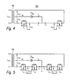
- Figur 4
- ein erstes Ausführungsbeispiel für ein Ladegerät zum Aufladen eines Akkumulators;
- Figur 5
- ein zweites Ausführungsbeispiel für ein Ladegerät zum Aufladen eines Akkumulators;
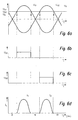
- Figur 6a
- die Verläufe einer ersten und einer zweiten Sekundärspannung auf der Sekundärseite eines Transformators mit Mittelanzapfung des Ladegeräts gemäß Figur 5;
- Figur 6b
- den Verlauf der Gatespannung UG1 gemäß Figur 5;
- Figur 6c
- den Verlauf der Gatespannung UG2 gemäß Figur 5;
- Figur 6d
- die Verläufe der Ladeströme in der beiden Zweigen der Gleichrichtereinrichtung des Ladegeräts Gemäß Figur 5;
- Figur 7
- ein Beispiel für eine Ansteuerung der Diodenschaltkreise in dem Ladegerät gemäß Figur 5;
- Figur 8a
- den Verlauf der Ausgangsspannung des ersten Operationsverstärkers OP1 gemäß Figur 7;
- Figur 8b
- den Verlauf der Ausgangsspannung des zweiten Operationsverstärkers OP2 gemäß Figur 7;
- Figur 8c
- den Verlauf eines Steuersignals S zur Ansteuerung der beiden Transistoren in Figur 7 und
- Figur 8d
- den Verlauf des Ladestroms durch einen Akkumulator, wenn dieser durch das erfindungsgemäße Ladegerät aufgeladen wird;
Claims (8)
- Elektronischer Diodenschaltkreis mit einer Anode (A) und einer Kathode (K), gekennzeichnet durch:mindestens einen zwischen die Anode und die Kathode geschalteten Feld-Effekt-Transistor FET (T1, T1a, T1b) mit einem Gate, einer Source und einer Drain, wobei die Kathode durch die Drain repräsentiert wird; und einen Operationsverstärker (OP1), dessen nicht-invertierender Eingang (+) an die Anode, dessen invertierender Eingang (-) an die Kathode und dessen Ausgang, erforderlichenfalls über einen Widerstand (R2),an das Gate des FET angeschlossen sind, zum Steuern des Betrages der Gatespannung (UG)nach Maßgabe durch die Potentialdifferenz zwischen der Anode und der Kathode.
- Elektronischer Diodenschaltkreis nach Anspruch 1,
dadurch gekennzeichnet, dass zwischen das Gate und die Source des FET eine Impedanz (R1) geschaltet ist. - Diodenschaltkreis nach Anspruch 1 oder 2, gekennzeichnet durch ein gesteuertes Schaltelement (Trs1, Trs2), insbesondere einen Transistor, welches zwischen das Gate des FET (T1, T1a, T1b) und die Anode des Diodenschaltkreises geschälter ist zum Sperren des FET (T1, T1a, Tb) durch Bereitstellen einer elektrisch leitenden Verbindung zwischen dem Gate (G) und der Anode (A) im Ansprechen auf ein Steuersignal (S).
- Dicdenschaltkreis nach einem der vorangegangenen Ansprüche, gekennzeichnet durch einen zweiten FET (T2), welcher mit seinem Gate an das Gate des ersten FET (T1), mit seiner Source an die Source des ersten FET (T1) angeschlossen ist und dessen Drain die Anode (A) repräsentiert.
- Diodenschaltkreis nach einem der vorangegangenen Ansprüche, dadurch gekennzeichnet, dass der Diodenschaltkreis auf einem Chip integriert ist.
- Gleichrichtereinrichtung zum Umwandeln einer Wechselspannung in eine Gleichspannung gekennzeichnet durch mindestens einen elektronischen Diodenschaltkreis gemäß einem der Ansprüche 1-5.
- Ladegerät (110) zum Aufladen eines Akkumulators, umfassend:dadurch gekennzeichnet, dasseinen primärseitig vorzugsweise netzgespeisten Transformator (110); undeine Gleichrichcereinrichtung auf der Sekundärseite des Transformators mit mindestens einem Diodenschaltkreis(T1, T2) zum Bereitstellen einer gleichgerichteten Ladespannung (Ub) für den aufzuladenden Akkumulator;
der Diodenschaltkreis gemäß einem der Ansprüche 1-5 ausgebildet ist. - Ladegerät (110) nach Anspruch 7, dadurch gekennzeichnet, dass die Sekundärwicklung des Transformators (110) eine Mittelanzapfung (M) aufweist zum Bereitstellen einer ersten Sekundärspannung (US1) zwischen der Mittelanzapfung und einem zweiten Endabgriff der Sekundärwicklung und einer zweiten Sekundärspannung (US2) zwischen der Mittelanzapfung und einem ersten Endabgriff der Sekundärwicklung;
die Gleichrichtereinrichtung zwei Diodenschaltkreise aufweist, wobei die Kathode eines ersten Diodenschal tkreises an die erste Endanzapfung und die Kathode eines zweiten Diodenschaltkreises an die zweite Endanzapfung angeschlossen ist und die Anoden der beiden Diodenschaltkreise zu einem Verbindungspunkt (V) zusammengeschaltet sind; und
wobei die Ladespannung (Ub) für den Akkumulator zwischen der Mittelanzapfung (M) und dem Verbindungspunkt (V) der beiden Anoden bereitsteht.
Applications Claiming Priority (2)
| Application Number | Priority Date | Filing Date | Title |
|---|---|---|---|
| DE10345929 | 2003-10-02 | ||
| DE10345929A DE10345929A1 (de) | 2003-10-02 | 2003-10-02 | Elektronischer Diodenschaltkreis |
Publications (2)
| Publication Number | Publication Date |
|---|---|
| EP1521354A2 true EP1521354A2 (de) | 2005-04-06 |
| EP1521354A3 EP1521354A3 (de) | 2006-01-04 |
Family
ID=34306235
Family Applications (1)
| Application Number | Title | Priority Date | Filing Date |
|---|---|---|---|
| EP20040018806 Withdrawn EP1521354A3 (de) | 2003-10-02 | 2004-08-07 | Synchrongleichrichter |
Country Status (2)
| Country | Link |
|---|---|
| EP (1) | EP1521354A3 (de) |
| DE (1) | DE10345929A1 (de) |
Cited By (6)
| Publication number | Priority date | Publication date | Assignee | Title |
|---|---|---|---|---|
| DE102005033477A1 (de) * | 2005-07-18 | 2007-01-25 | Austriamicrosystems Ag | Schaltungsanordnung und Verfahren zum Konvertieren einer Wechselspannung in eine gleichgerichtete Spannung |
| WO2009077257A1 (de) * | 2007-12-14 | 2009-06-25 | Robert Bosch Gmbh | Gleichrichterschaltung |
| US7755327B2 (en) | 2006-11-08 | 2010-07-13 | Shenzhen Mindray Bio-Medical Electronics Co., Ltd. | Synchronous rectification type battery charging circuit and protection circuit thereof |
| CN101976938A (zh) * | 2010-09-20 | 2011-02-16 | 石家庄国耀电子科技有限公司 | 一种运行稳定可靠的大电流低压降单向导电电路 |
| WO2011029953A1 (de) * | 2009-09-14 | 2011-03-17 | Tridonic Ag | Betriebsgerät für leuchtmittel |
| EP2533424A1 (de) * | 2011-06-07 | 2012-12-12 | Hamilton Sundstrand Corporation | Halbleiterschalteranordnung |
Families Citing this family (1)
| Publication number | Priority date | Publication date | Assignee | Title |
|---|---|---|---|---|
| DE102007046705B3 (de) | 2007-09-28 | 2009-04-30 | Infineon Technologies Austria Ag | Schaltung für eine aktive Diode und Verfahren zum Betrieb einer aktiven Diode |
Family Cites Families (4)
| Publication number | Priority date | Publication date | Assignee | Title |
|---|---|---|---|---|
| WO1997047071A1 (fr) * | 1996-06-05 | 1997-12-11 | Ntt Data Corporation | Circuit electrique |
| US6212084B1 (en) * | 1999-05-17 | 2001-04-03 | Page Aerospace Limited | Active rectifier |
| US6288919B1 (en) * | 1999-12-16 | 2001-09-11 | Chippower.Com, Inc. | Single stage AC/DC converter high frequency AC distribution systems |
| EP1388208B1 (de) * | 2001-03-28 | 2007-01-10 | Koninklijke Philips Electronics N.V. | Sychrongleichrichter |
-
2003
- 2003-10-02 DE DE10345929A patent/DE10345929A1/de not_active Withdrawn
-
2004
- 2004-08-07 EP EP20040018806 patent/EP1521354A3/de not_active Withdrawn
Cited By (13)
| Publication number | Priority date | Publication date | Assignee | Title |
|---|---|---|---|---|
| DE102005033477A1 (de) * | 2005-07-18 | 2007-01-25 | Austriamicrosystems Ag | Schaltungsanordnung und Verfahren zum Konvertieren einer Wechselspannung in eine gleichgerichtete Spannung |
| DE102005033477B4 (de) * | 2005-07-18 | 2016-02-04 | Austriamicrosystems Ag | Schaltungsanordnung und Verfahren zum Konvertieren einer Wechselspannung in eine gleichgerichtete Spannung |
| US8134847B2 (en) | 2005-07-18 | 2012-03-13 | Austriamicrosystems Ag | Circuit arrangement and method for converting an alternating voltage into a rectified voltage |
| US7755327B2 (en) | 2006-11-08 | 2010-07-13 | Shenzhen Mindray Bio-Medical Electronics Co., Ltd. | Synchronous rectification type battery charging circuit and protection circuit thereof |
| WO2009077257A1 (de) * | 2007-12-14 | 2009-06-25 | Robert Bosch Gmbh | Gleichrichterschaltung |
| US8427801B2 (en) | 2007-12-14 | 2013-04-23 | Robert Bosch Gmbh | Rectifier circuit |
| CN102577064A (zh) * | 2009-09-14 | 2012-07-11 | 特里多尼克股份有限公司 | 用于照明器件的运行设备 |
| WO2011029953A1 (de) * | 2009-09-14 | 2011-03-17 | Tridonic Ag | Betriebsgerät für leuchtmittel |
| CN102577064B (zh) * | 2009-09-14 | 2014-10-29 | 特里多尼克股份有限公司 | 用于照明器件的运行设备 |
| CN101976938B (zh) * | 2010-09-20 | 2013-01-23 | 石家庄国耀电子科技有限公司 | 一种运行稳定可靠的大电流低压降单向导电电路 |
| CN101976938A (zh) * | 2010-09-20 | 2011-02-16 | 石家庄国耀电子科技有限公司 | 一种运行稳定可靠的大电流低压降单向导电电路 |
| EP2533424A1 (de) * | 2011-06-07 | 2012-12-12 | Hamilton Sundstrand Corporation | Halbleiterschalteranordnung |
| US8587146B2 (en) | 2011-06-07 | 2013-11-19 | Hamilton Sundstrand Corporation | Solid state contactor assembly |
Also Published As
| Publication number | Publication date |
|---|---|
| EP1521354A3 (de) | 2006-01-04 |
| DE10345929A1 (de) | 2005-04-21 |
Similar Documents
| Publication | Publication Date | Title |
|---|---|---|
| DE102019206970B4 (de) | Mehrstufen-Leistungsumsetzer mit Regelung der Spannung des massefreien Kondensators bei Schwachlast | |
| EP0423885B1 (de) | Stromversorgungseinrichtung mit Einschaltstrombegrenzungsschaltung | |
| DE10046668B4 (de) | Elektrische Lastansteuerungsschaltung mit Schutzeinrichtung | |
| DE69834981T2 (de) | Phasenversetzter Vollbrückenwandler mit sanfter PWM-Umschaltung | |
| DE60301054T2 (de) | Mehrzelliger gleichspannungswandler mit schutzschaltern | |
| DE3877326T2 (de) | Leistungsversorgung. | |
| DE112013005027B4 (de) | Flyback-Converter-Schaltung | |
| DE102006029475A1 (de) | Effiziente Einschaltstrom-Begrenzungsschaltung mit bidirektionellen Doppelgate-HEMT-Bauteilen | |
| DE19861384B4 (de) | Gleichspannungskonverter mit einer Schaltungsanordnung zum Verhindern einer Querleitung | |
| DE1763820A1 (de) | Gleichspannungs-Gleichspannungs-Wandler | |
| DE102014106417A1 (de) | Systeme und Verfahren zum Eliminieren von Übergangsverlusten in DC-DC-Wandlern | |
| WO1991016756A1 (de) | Gleichstromumrichter mit strombegrenzung | |
| DE102015112245A1 (de) | Gleichrichter mit spannungsdetektion | |
| DE102019214978A1 (de) | Hybrid-Mehrpegel-Leistungsumsetzer mit Umgehung durch ein induktives Bauelement | |
| DE102020212477A1 (de) | Hybridwandler mit impliziter Ein-Zeit-Regelung | |
| DE102011087431A1 (de) | Anordnung und Verfahren zum Treiben eines Kaskodenschalters | |
| EP0342693B1 (de) | Gleichspannungsversorgungssystem mit mehreren Gleichspannungsquellen | |
| EP0943974B1 (de) | Spannungsregelschaltung | |
| EP3316463A1 (de) | Ändern eines schaltzustands einer schalt-halbbrücke | |
| EP1521354A2 (de) | Synchrongleichrichter | |
| EP1658676B1 (de) | Schaltung und verfahren zum verarbeiten einer speisespannung mit spannungsspitzen | |
| EP2208400A1 (de) | Umschaltbare spannungsversorgung für hilfsstromkreise in einem stromrichter | |
| DE2108101B2 (de) | Schalterstromkrels | |
| DE3031197A1 (de) | Antriebsschaltkreis | |
| EP1078460B1 (de) | Verfahren und vorrichtung zum umschalten eines feldeffekttransistors |
Legal Events
| Date | Code | Title | Description |
|---|---|---|---|
| PUAI | Public reference made under article 153(3) epc to a published international application that has entered the european phase |
Free format text: ORIGINAL CODE: 0009012 |
|
| AK | Designated contracting states |
Kind code of ref document: A2 Designated state(s): AT BE BG CH CY CZ DE DK EE ES FI FR GB GR HU IE IT LI LU MC NL PL PT RO SE SI SK TR |
|
| AX | Request for extension of the european patent |
Extension state: AL HR LT LV MK |
|
| PUAL | Search report despatched |
Free format text: ORIGINAL CODE: 0009013 |
|
| AK | Designated contracting states |
Kind code of ref document: A3 Designated state(s): AT BE BG CH CY CZ DE DK EE ES FI FR GB GR HU IE IT LI LU MC NL PL PT RO SE SI SK TR |
|
| AX | Request for extension of the european patent |
Extension state: AL HR LT LV MK |
|
| 17P | Request for examination filed |
Effective date: 20060704 |
|
| AKX | Designation fees paid |
Designated state(s): DE ES FR GB IT |
|
| 17Q | First examination report despatched |
Effective date: 20150421 |
|
| STAA | Information on the status of an ep patent application or granted ep patent |
Free format text: STATUS: THE APPLICATION IS DEEMED TO BE WITHDRAWN |
|
| 18D | Application deemed to be withdrawn |
Effective date: 20150901 |