EP1521189B1 - Formale Beweismethoden zur Analyse von Schaltungsbelastungsproblemen unter Betriebsbedingungen - Google Patents
Formale Beweismethoden zur Analyse von Schaltungsbelastungsproblemen unter Betriebsbedingungen Download PDFInfo
- Publication number
- EP1521189B1 EP1521189B1 EP04292204.7A EP04292204A EP1521189B1 EP 1521189 B1 EP1521189 B1 EP 1521189B1 EP 04292204 A EP04292204 A EP 04292204A EP 1521189 B1 EP1521189 B1 EP 1521189B1
- Authority
- EP
- European Patent Office
- Prior art keywords
- logic
- driving
- node
- loads
- circuit
- Prior art date
- Legal status (The legal status is an assumption and is not a legal conclusion. Google has not performed a legal analysis and makes no representation as to the accuracy of the status listed.)
- Expired - Lifetime
Links
Images


Classifications
-
- G—PHYSICS
- G06—COMPUTING OR CALCULATING; COUNTING
- G06F—ELECTRIC DIGITAL DATA PROCESSING
- G06F30/00—Computer-aided design [CAD]
- G06F30/30—Circuit design
- G06F30/32—Circuit design at the digital level
- G06F30/327—Logic synthesis; Behaviour synthesis, e.g. mapping logic, HDL to netlist, high-level language to RTL or netlist
-
- G—PHYSICS
- G06—COMPUTING OR CALCULATING; COUNTING
- G06F—ELECTRIC DIGITAL DATA PROCESSING
- G06F30/00—Computer-aided design [CAD]
- G06F30/30—Circuit design
- G06F30/32—Circuit design at the digital level
- G06F30/33—Design verification, e.g. functional simulation or model checking
- G06F30/3323—Design verification, e.g. functional simulation or model checking using formal methods, e.g. equivalence checking or property checking
Definitions
- This invention relates to the art of logic design and implementation and, more particularly, to a tool for determining if any driving node in a very complex logic circuit, such as a processor, has suitable power handling capacity to drive its collective loads under "real", rather than "worst-case” assumed, conditions.
- Modern integrated circuits have become very dense and complex.
- state-of-the art integrated circuits constituting processors may each include many millions of transistors and other components.
- checking the resulting logic equations of, for example, a processor for subtle errors is a very daunting problem which is impossible to carry out manually and difficult to achieve with any test software.
- formal proof is used herein as a generic term for these types of programs.
- formal proof programs may still take a long time to analyze all combinations of the reduced logic, the time is not prohibitive for use during the development and analysis of a complex logic component.
- this absolute worst-case assumed solution may be much too pessimistic in that, in all "real" possible combinations for a given driving node, some of the loads may be through transistors which are not enabled such that the actual worst case loading might be less or even much less.
- This characteristic leads to warnings or error reports, from circuit analysis programs, which are in fact not "real” or possible during the actual operation of the logic circuit.
- the logic even of a single driving node may be too complicated to analyze easily by hand, and/or the number of warnings/errors reported may obscure the recognition of "real" errors; i.e., the important message may be buried in a report containing a large number of "false” errors.
- an exemplary node includes a driver 1 and loads 3, 5, 7, 9 selectively imposed on driver 1 according to the input status of pass transistors 2, 4, 6, 8.
- the pass transistors are individually enabled by suitable signals applied to their respective gates 2G, 4G, 6G, 8G.
- FIG. 2 shows a second exemplary node in which the load 7 may be imposed on the driver 1 if either or both control transistors 6A, 6B are enabled.
- the driver nodes shown in FIGs. 1 and 2 are representative of circuits widely found in complex logic, and the transistors are typically input stages to certain types of logic elements such as latches, switches, multiplexers, etc. Often, an individual driver will selectively provide switching current to more than four loads as shown, but this is a sufficient number to explain the invention.
- a logic equation generation and analysis software tool is used to extract logic equations from a circuit description.
- the software tool "Circuit” (from Bull Worldwide Information Systems) will perform this function.
- the logic equations generated by Circuit and equivalent software tools will identify and configure driver nodes along with other logic and will provide a certain amount of analysis such as determining how many loads are driven by a given driving node.
- the "real" loading is not determinable by such tools, and therefore, the worst case is assumed with the resulting drawbacks discussed above.
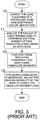
- FIG. 3 is a process flow chart according to the prior art.
- the software tool extracts the logic equations for a given logic circuit from a circuit description.
- the software tool (or another suitable software tool) analyzes the fan-out of every driving node to determine the amount of loading driven by each node, some or all of which may be loading "through" pass transistors.
- the software tool marks each node which has potentially too many loads. That is, a standard driver capable of driving a predetermined number of loads may be assumed for all drivers or for each of a class of drivers. Thus, if a given driver node, such as the driver 1 of the nodes shown in FIGs.
- the drive handling capacity specification for the given node is adjusted higher such that, when the circuit is implemented in hardware, the worst case condition can be handled.
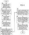
- step 20 use a software tool which extracts the logic equations for a given logic circuit from a circuit description, step 20. Then, also as in the prior art, analyze, at step 21, the fan-out of every driving node to determine the total number of pass transistor loads driven by each node. At step 22, also as in the prior art, flag each node which has potentially too many loads (for an assumed "standard” driver which has a predetermined load driving capacity which is less than "worst case").
- Step 23 begins a fundamental departure from the prior art. During step 23, for those nodes identified as having potentially too many loads, equations are added to the circuit's logic description to represent the sum of the loads through all transistors that are "turned on”.
- a formal proof program is used, for each identified node, to analyze the supplemented logic equations and determine which of the loading comparative equations described in step 24 can have a true output for any signal input combination (for the entire component including a currently analyzed node) in which the currently analyzed node can be active. If the output of the loading comparative equation described in step 24 can never be true, then the condition cannot logically exist and therefore need not be considered with respect to a node's driving capacity requirements. The important consideration is thus which is the largest value of loading which might possibly be seen by the driver, and is represented by largest of the four loading comparitive equations might ever be true.
- step 22 assume that the driver 1 of FIG. 1 is preliminarily established as capable of driving three unit loads simultaneously, but it was found in step 22 that there were potentially four loads on driving gate 1. Without this new methodology, the driving capacity of gate 1 would have to be enlarged to provide for a capacity of four.
- the process might determine that the highest load to which the driving node might be subjected is only two so it would be found not to be necessary to increase the driving strength of the driver 1 accordingly (in this example, to full "worst case”) and indeed the driving capacity could be reduced to a driver for gate 1 capable of driving only two units of loading.
- the average size of driving nodes in a component can be substantially reduced to achieve the objects set forth above.
Landscapes
- Engineering & Computer Science (AREA)
- Computer Hardware Design (AREA)
- Physics & Mathematics (AREA)
- Theoretical Computer Science (AREA)
- Evolutionary Computation (AREA)
- Geometry (AREA)
- General Engineering & Computer Science (AREA)
- General Physics & Mathematics (AREA)
- Design And Manufacture Of Integrated Circuits (AREA)
- Tests Of Electronic Circuits (AREA)
- Logic Circuits (AREA)
Claims (5)
- Verfahren zum Bestimmen der optimalen Lastansteuerungskapazität für einen Ansteuerungsknoten mit einer gegebenen Gesamtzahl von Durchgangstransistorlasten in einer Logikschaltung, das die folgenden Schritte umfasst:A) Extrahieren (20) der Logikgleichungen der Logikschaltung aus einer Schaltungsbeschreibung davon;B) Analysieren (21) des Fan-out des Ansteuerungsknotens, um zu bestimmen (22), ob die Gesamtzahl der Durchgangstransistorlasten verglichen mit einer vorbestimmten Lastansteuerungskapazität des Ansteuerungsknotens überhöht ist;dadurch gekennzeichnet, dass es ferner die folgenden Schritte umfasst:C) wenn bei Schritt B) bestimmt wird (22), dass die Gesamtzahl der Durchgangstransistorlasten die vorbestimmte Lastansteuerungskapazität übersteigt, dann:1) Hinzufügen (23) von Logikgleichungen, die die Summe der Lasten durch die Durchgangstransistoren, die eingeschaltet sind, repräsentieren, zu den extrahierten Logikgleichungen der Logikschaltung;2) ferner Hinzufügen von Komparatorlogikgleichungen zu den extrahierten Logikgleichungen der Logikschaltung zum Vergleichen (24) einer Menge der Summe der Lasten durch die Durchgangstransistoren, die eingeschaltet sind, wobei jede Last einer Anzahl der eingeschalteten Durchgangstransistoren entspricht, wobei sich die Anzahl von einem bis zur Gesamtzahl von Durchgangstransistorlasten erhöht, wobei jede Komparatorlogikgleichung einen wahren Ausgang aufweist, wenn und nur wenn die Menge der Summe von Lasten durch die Durchgangstransistoren, die eingeschaltet sind, größer ist als die Last, die der Anzahl von eingeschalteten Durchgangstransistoren dieser Komparatorlogikgleichung entspricht;3) Verwenden (25) eines formalen Beweisprogramms, um die hinzugefügten Logikgleichungen der Schritte C.1) und C.2) zu analysieren, daher Bestimmen, welche der Komparatorlogikgleichungen von Schritt C.2) für jede Signaleingangskombination, bei der der Ansteuerungsknoten aktiv sein kann, einen wahren Ausgang haben kann;4) Identifizieren (26) der Komparatorlogikgleichung, die der größten Anzahl von eingeschalteten Durchgangstransistoren entspricht, die einen wahren Ausgang haben kann, wie in Schritt C.3) bestimmt, um die höchste mögliche tatsächliche Last zu bestimmen; und5) sofern erforderlich, Anpassen (27) der Lastansteuerungskapazität des Ansteuerungsknotens, um die bestimmte höchste mögliche tatsächliche Last zu bewältigen.
- Verfahren nach Anspruch 1, das für jeden Ansteuerungsknoten, von denen jeder eine gegebene Gesamtzahl von Durchgangstransistorlasten aufweist, in einer komplexen Logikschaltung mit mehreren Ansteuerungsknoten durchgeführt wird, wobei: - jeder Ansteuerungsknoten, für den in Schritt B bestimmt wird, dass seine Gesamtzahl von Durchgangstransistorlasten verglichen mit einer vorbestimmten Lastansteuerungskapazität jedes der Ansteuerungsknoten überhöht ist, markiert wird; - Schritt C für jeden Ansteuerungsknoten durchgeführt wird, der in Schritt B markiert wurde.
- Verfahren nach Anspruch 1 oder 2, wobei das Extrahieren der Logikgleichungen der Logikschaltung von einem Programm entwickelt wird, das eine Logikbeschreibung aus einer elektronischen Beschreibung der Schaltung extrahiert, die die Verbindung von Transistoren und anderen elektronischen Elementen beschreibt.
- Verfahren nach Anspruch 3, das den hinzugefügten Schritt beinhaltet, bei dem die elektronische Schaltung geändert wird, um die Lastansteuerungskapazität von mindestens einem Knoten auf Basis der Ergebnisse des formalen Beweisprogramms anzupassen.
- Verfahren nach einem der Ansprüche 1 bis 4, wobei die hinzugefügten Logikgleichungen zum Angeben und Berechnen der Belastung ganzzahlige Werte einsetzen.
Applications Claiming Priority (2)
| Application Number | Priority Date | Filing Date | Title |
|---|---|---|---|
| US675851 | 2003-09-30 | ||
| US10/675,851 US6983429B2 (en) | 2003-09-30 | 2003-09-30 | Formal proof methods for analyzing circuit loading problems under operating conditions |
Publications (3)
| Publication Number | Publication Date |
|---|---|
| EP1521189A2 EP1521189A2 (de) | 2005-04-06 |
| EP1521189A3 EP1521189A3 (de) | 2007-02-14 |
| EP1521189B1 true EP1521189B1 (de) | 2018-05-02 |
Family
ID=34314015
Family Applications (1)
| Application Number | Title | Priority Date | Filing Date |
|---|---|---|---|
| EP04292204.7A Expired - Lifetime EP1521189B1 (de) | 2003-09-30 | 2004-09-14 | Formale Beweismethoden zur Analyse von Schaltungsbelastungsproblemen unter Betriebsbedingungen |
Country Status (2)
| Country | Link |
|---|---|
| US (1) | US6983429B2 (de) |
| EP (1) | EP1521189B1 (de) |
Families Citing this family (8)
| Publication number | Priority date | Publication date | Assignee | Title |
|---|---|---|---|---|
| SE533007C2 (sv) | 2008-10-24 | 2010-06-08 | Ilt Productions Ab | Distribuerad datalagring |
| EP2712149B1 (de) | 2010-04-23 | 2019-10-30 | Compuverde AB | Verteilte datenspeicherung |
| US8997124B2 (en) | 2011-09-02 | 2015-03-31 | Compuverde Ab | Method for updating data in a distributed data storage system |
| US8645978B2 (en) | 2011-09-02 | 2014-02-04 | Compuverde Ab | Method for data maintenance |
| US9021053B2 (en) | 2011-09-02 | 2015-04-28 | Compuverde Ab | Method and device for writing data to a data storage system comprising a plurality of data storage nodes |
| US9626378B2 (en) | 2011-09-02 | 2017-04-18 | Compuverde Ab | Method for handling requests in a storage system and a storage node for a storage system |
| US8650365B2 (en) | 2011-09-02 | 2014-02-11 | Compuverde Ab | Method and device for maintaining data in a data storage system comprising a plurality of data storage nodes |
| US8769138B2 (en) | 2011-09-02 | 2014-07-01 | Compuverde Ab | Method for data retrieval from a distributed data storage system |
Family Cites Families (2)
| Publication number | Priority date | Publication date | Assignee | Title |
|---|---|---|---|---|
| JP3019020B2 (ja) * | 1997-03-28 | 2000-03-13 | 日本電気株式会社 | 回路設計方法およびシステム |
| US6886152B1 (en) * | 2002-08-09 | 2005-04-26 | Xilinx, Inc. | Delay optimization in signal routing |
-
2003
- 2003-09-30 US US10/675,851 patent/US6983429B2/en not_active Expired - Lifetime
-
2004
- 2004-09-14 EP EP04292204.7A patent/EP1521189B1/de not_active Expired - Lifetime
Non-Patent Citations (1)
| Title |
|---|
| None * |
Also Published As
| Publication number | Publication date |
|---|---|
| US20050071793A1 (en) | 2005-03-31 |
| EP1521189A2 (de) | 2005-04-06 |
| US6983429B2 (en) | 2006-01-03 |
| EP1521189A3 (de) | 2007-02-14 |
Similar Documents
| Publication | Publication Date | Title |
|---|---|---|
| US6952812B2 (en) | Design analysis tool for path extraction and false path identification and method thereof | |
| US5657240A (en) | Testing and removal of redundancies in VLSI circuits with non-boolean primitives | |
| JPH04101274A (ja) | 論理設計処理装置およびタイミング調整方法 | |
| US11704460B2 (en) | System and method for fast and accurate netlist to RTL reverse engineering | |
| US6983429B2 (en) | Formal proof methods for analyzing circuit loading problems under operating conditions | |
| US6192505B1 (en) | Method and system for reducing state space variables prior to symbolic model checking | |
| US8302048B2 (en) | Method and apparatus for detecting contradictory timing constraint conflicts | |
| CN116187237A (zh) | 用于芯片设计的检查方法、设备及介质 | |
| WO2004077260A2 (en) | Method and apparatus for creating circuit redundancy in programmable logic devices | |
| US20040216069A1 (en) | Method of designing low-power semiconductor integrated circuit | |
| Brunner et al. | Toward a human-readable state machine extraction | |
| US6317861B1 (en) | Delay verification device for logic circuit and delay verification method therefor | |
| US7152214B2 (en) | Recognition of a state machine in high-level integrated circuit description language code | |
| CN113051858A (zh) | 基于子图同构的fpga软件可疑电路检测方法 | |
| CN108279595A (zh) | 用于控制设备机组状态的方法、装置和设备机组 | |
| US6631506B1 (en) | Method and apparatus for identifying switching race conditions in a circuit design | |
| US7134107B1 (en) | System and method for determining detail of analysis in a circuit design | |
| US6871308B1 (en) | Semiconductor inspection method | |
| Iyer et al. | Surprises in sequential redundancy identification | |
| JP2560800B2 (ja) | 諭理回路検証装置 | |
| US6728938B2 (en) | Knowledge-based intelligent full scan dump processing methodology | |
| Rahardjo | SPIN as a hardware design tool | |
| US20230394206A1 (en) | Method for designing fault detection circuit | |
| Debreil et al. | Synchronous designs in VHDL | |
| WO2008062571A1 (en) | Circuit test apparatus for semiconductor integrated circuit |
Legal Events
| Date | Code | Title | Description |
|---|---|---|---|
| PUAI | Public reference made under article 153(3) epc to a published international application that has entered the european phase |
Free format text: ORIGINAL CODE: 0009012 |
|
| AK | Designated contracting states |
Kind code of ref document: A2 Designated state(s): AT BE BG CH CY CZ DE DK EE ES FI FR GB GR HU IE IT LI LU MC NL PL PT RO SE SI SK TR |
|
| AX | Request for extension of the european patent |
Extension state: AL HR LT LV MK |
|
| PUAL | Search report despatched |
Free format text: ORIGINAL CODE: 0009013 |
|
| AK | Designated contracting states |
Kind code of ref document: A3 Designated state(s): AT BE BG CH CY CZ DE DK EE ES FI FR GB GR HU IE IT LI LU MC NL PL PT RO SE SI SK TR |
|
| AX | Request for extension of the european patent |
Extension state: AL HR LT LV MK |
|
| 17P | Request for examination filed |
Effective date: 20070628 |
|
| AKX | Designation fees paid |
Designated state(s): DE FR GB IT |
|
| 17Q | First examination report despatched |
Effective date: 20130808 |
|
| GRAP | Despatch of communication of intention to grant a patent |
Free format text: ORIGINAL CODE: EPIDOSNIGR1 |
|
| STAA | Information on the status of an ep patent application or granted ep patent |
Free format text: STATUS: GRANT OF PATENT IS INTENDED |
|
| INTG | Intention to grant announced |
Effective date: 20180207 |
|
| GRAS | Grant fee paid |
Free format text: ORIGINAL CODE: EPIDOSNIGR3 |
|
| GRAA | (expected) grant |
Free format text: ORIGINAL CODE: 0009210 |
|
| STAA | Information on the status of an ep patent application or granted ep patent |
Free format text: STATUS: THE PATENT HAS BEEN GRANTED |
|
| AK | Designated contracting states |
Kind code of ref document: B1 Designated state(s): DE FR GB IT |
|
| REG | Reference to a national code |
Ref country code: GB Ref legal event code: FG4D |
|
| REG | Reference to a national code |
Ref country code: DE Ref legal event code: R096 Ref document number: 602004052657 Country of ref document: DE |
|
| RAP2 | Party data changed (patent owner data changed or rights of a patent transferred) |
Owner name: ATOS IT SOLUTIONS AND SERVICES INC. |
|
| REG | Reference to a national code |
Ref country code: DE Ref legal event code: R097 Ref document number: 602004052657 Country of ref document: DE |
|
| PLBE | No opposition filed within time limit |
Free format text: ORIGINAL CODE: 0009261 |
|
| STAA | Information on the status of an ep patent application or granted ep patent |
Free format text: STATUS: NO OPPOSITION FILED WITHIN TIME LIMIT |
|
| 26N | No opposition filed |
Effective date: 20190205 |
|
| PGFP | Annual fee paid to national office [announced via postgrant information from national office to epo] |
Ref country code: IT Payment date: 20190923 Year of fee payment: 16 |
|
| REG | Reference to a national code |
Ref country code: DE Ref legal event code: R079 Ref document number: 602004052657 Country of ref document: DE Free format text: PREVIOUS MAIN CLASS: G06F0017500000 Ipc: G06F0030000000 |
|
| PG25 | Lapsed in a contracting state [announced via postgrant information from national office to epo] |
Ref country code: IT Free format text: LAPSE BECAUSE OF NON-PAYMENT OF DUE FEES Effective date: 20200914 |
|
| P01 | Opt-out of the competence of the unified patent court (upc) registered |
Effective date: 20230330 |
|
| PGFP | Annual fee paid to national office [announced via postgrant information from national office to epo] |
Ref country code: GB Payment date: 20230921 Year of fee payment: 20 |
|
| PGFP | Annual fee paid to national office [announced via postgrant information from national office to epo] |
Ref country code: FR Payment date: 20230918 Year of fee payment: 20 Ref country code: DE Payment date: 20230919 Year of fee payment: 20 |
|
| REG | Reference to a national code |
Ref country code: DE Ref legal event code: R071 Ref document number: 602004052657 Country of ref document: DE |
|
| REG | Reference to a national code |
Ref country code: GB Ref legal event code: PE20 Expiry date: 20240913 |
|
| PG25 | Lapsed in a contracting state [announced via postgrant information from national office to epo] |
Ref country code: GB Free format text: LAPSE BECAUSE OF EXPIRATION OF PROTECTION Effective date: 20240913 |
|
| PG25 | Lapsed in a contracting state [announced via postgrant information from national office to epo] |
Ref country code: GB Free format text: LAPSE BECAUSE OF EXPIRATION OF PROTECTION Effective date: 20240913 |