EP1520186B1 - A multi-layered radiation converter - Google Patents
A multi-layered radiation converter Download PDFInfo
- Publication number
- EP1520186B1 EP1520186B1 EP03741726A EP03741726A EP1520186B1 EP 1520186 B1 EP1520186 B1 EP 1520186B1 EP 03741726 A EP03741726 A EP 03741726A EP 03741726 A EP03741726 A EP 03741726A EP 1520186 B1 EP1520186 B1 EP 1520186B1
- Authority
- EP
- European Patent Office
- Prior art keywords
- converter
- radiation
- layers
- electrons
- photons
- Prior art date
- Legal status (The legal status is an assumption and is not a legal conclusion. Google has not performed a legal analysis and makes no representation as to the accuracy of the status listed.)
- Expired - Lifetime
Links
- 230000005855 radiation Effects 0.000 title claims abstract description 179
- 238000006243 chemical reaction Methods 0.000 claims abstract description 22
- 230000003993 interaction Effects 0.000 claims abstract description 18
- 238000003384 imaging method Methods 0.000 claims abstract description 15
- 238000010521 absorption reaction Methods 0.000 claims abstract description 6
- 238000012545 processing Methods 0.000 claims description 22
- XQPRBTXUXXVTKB-UHFFFAOYSA-M caesium iodide Chemical compound [I-].[Cs+] XQPRBTXUXXVTKB-UHFFFAOYSA-M 0.000 claims description 19
- 238000005229 chemical vapour deposition Methods 0.000 claims description 13
- 239000010432 diamond Substances 0.000 claims description 13
- 229910003460 diamond Inorganic materials 0.000 claims description 13
- 239000011810 insulating material Substances 0.000 claims description 9
- 230000005684 electric field Effects 0.000 claims description 6
- 239000007789 gas Substances 0.000 description 35
- 238000001514 detection method Methods 0.000 description 11
- 239000007787 solid Substances 0.000 description 9
- 230000001225 therapeutic effect Effects 0.000 description 8
- 206010028980 Neoplasm Diseases 0.000 description 6
- 239000005355 lead glass Substances 0.000 description 6
- 238000001465 metallisation Methods 0.000 description 6
- 238000001959 radiotherapy Methods 0.000 description 6
- 238000002560 therapeutic procedure Methods 0.000 description 6
- 238000002059 diagnostic imaging Methods 0.000 description 5
- 238000000034 method Methods 0.000 description 5
- 238000013461 design Methods 0.000 description 4
- 230000000694 effects Effects 0.000 description 4
- 239000002184 metal Substances 0.000 description 4
- 229910052751 metal Inorganic materials 0.000 description 4
- RYGMFSIKBFXOCR-UHFFFAOYSA-N Copper Chemical compound [Cu] RYGMFSIKBFXOCR-UHFFFAOYSA-N 0.000 description 3
- 238000013459 approach Methods 0.000 description 3
- 201000011510 cancer Diseases 0.000 description 3
- 229910052802 copper Inorganic materials 0.000 description 3
- 239000010949 copper Substances 0.000 description 3
- 238000010586 diagram Methods 0.000 description 3
- 238000000605 extraction Methods 0.000 description 3
- 239000010437 gem Substances 0.000 description 3
- VNWKTOKETHGBQD-UHFFFAOYSA-N methane Chemical compound C VNWKTOKETHGBQD-UHFFFAOYSA-N 0.000 description 3
- 239000000203 mixture Substances 0.000 description 3
- 239000002245 particle Substances 0.000 description 3
- 230000009286 beneficial effect Effects 0.000 description 2
- 239000004020 conductor Substances 0.000 description 2
- 238000000151 deposition Methods 0.000 description 2
- 230000008021 deposition Effects 0.000 description 2
- 238000004519 manufacturing process Methods 0.000 description 2
- 238000009659 non-destructive testing Methods 0.000 description 2
- 210000000056 organ Anatomy 0.000 description 2
- 239000002243 precursor Substances 0.000 description 2
- 125000006850 spacer group Chemical group 0.000 description 2
- 210000001519 tissue Anatomy 0.000 description 2
- 229920002799 BoPET Polymers 0.000 description 1
- OKTJSMMVPCPJKN-UHFFFAOYSA-N Carbon Chemical compound [C] OKTJSMMVPCPJKN-UHFFFAOYSA-N 0.000 description 1
- UFHFLCQGNIYNRP-UHFFFAOYSA-N Hydrogen Chemical compound [H][H] UFHFLCQGNIYNRP-UHFFFAOYSA-N 0.000 description 1
- 239000005041 Mylar™ Substances 0.000 description 1
- 230000003213 activating effect Effects 0.000 description 1
- 230000001154 acute effect Effects 0.000 description 1
- 229910021417 amorphous silicon Inorganic materials 0.000 description 1
- 230000003321 amplification Effects 0.000 description 1
- 238000005452 bending Methods 0.000 description 1
- 210000000988 bone and bone Anatomy 0.000 description 1
- 229910052799 carbon Inorganic materials 0.000 description 1
- 239000011248 coating agent Substances 0.000 description 1
- 238000000576 coating method Methods 0.000 description 1
- 230000000295 complement effect Effects 0.000 description 1
- 239000002131 composite material Substances 0.000 description 1
- 238000002591 computed tomography Methods 0.000 description 1
- 238000011161 development Methods 0.000 description 1
- 230000018109 developmental process Effects 0.000 description 1
- 238000009792 diffusion process Methods 0.000 description 1
- 238000005516 engineering process Methods 0.000 description 1
- 239000010408 film Substances 0.000 description 1
- 238000001914 filtration Methods 0.000 description 1
- 239000003292 glue Substances 0.000 description 1
- 229910052739 hydrogen Inorganic materials 0.000 description 1
- 239000001257 hydrogen Substances 0.000 description 1
- 238000003780 insertion Methods 0.000 description 1
- 230000037431 insertion Effects 0.000 description 1
- 230000001678 irradiating effect Effects 0.000 description 1
- 229910052743 krypton Inorganic materials 0.000 description 1
- 239000000463 material Substances 0.000 description 1
- LCGLNKUTAGEVQW-UHFFFAOYSA-N methyl monoether Natural products COC LCGLNKUTAGEVQW-UHFFFAOYSA-N 0.000 description 1
- 229910052754 neon Inorganic materials 0.000 description 1
- 229910052756 noble gas Inorganic materials 0.000 description 1
- 150000002835 noble gases Chemical class 0.000 description 1
- 238000003199 nucleic acid amplification method Methods 0.000 description 1
- 230000000149 penetrating effect Effects 0.000 description 1
- 229920003223 poly(pyromellitimide-1,4-diphenyl ether) Polymers 0.000 description 1
- 239000002861 polymer material Substances 0.000 description 1
- 238000010791 quenching Methods 0.000 description 1
- 230000000171 quenching effect Effects 0.000 description 1
- 238000011160 research Methods 0.000 description 1
- 239000000758 substrate Substances 0.000 description 1
- 239000010409 thin film Substances 0.000 description 1
- 238000012795 verification Methods 0.000 description 1
Images


Classifications
-
- G—PHYSICS
- G01—MEASURING; TESTING
- G01T—MEASUREMENT OF NUCLEAR OR X-RADIATION
- G01T1/00—Measuring X-radiation, gamma radiation, corpuscular radiation, or cosmic radiation
- G01T1/29—Measurement performed on radiation beams, e.g. position or section of the beam; Measurement of spatial distribution of radiation
- G01T1/2914—Measurement of spatial distribution of radiation
- G01T1/2921—Static instruments for imaging the distribution of radioactivity in one or two dimensions; Radio-isotope cameras
- G01T1/2935—Static instruments for imaging the distribution of radioactivity in one or two dimensions; Radio-isotope cameras using ionisation detectors
Definitions
- the present invention generally concerns radiation converters and radiation detectors, and more particularly the use of such converters and detectors in radiation-based imaging systems for applications such as medical imaging and non-destructive testing.
- Radiation detectors are used for detection of incoming radiation such as X-rays, gamma photons and charged/uncharged particles, in a wide range of different applications.
- the incoming photons are converted to electrons through electromagnetic interactions, including the photoelectric effect, pair production and the Compton effect.
- the emitted electrons are normally multiplied by a multiplication structure to produce a multiplicity of secondary electrons and/or photons, which in turn may be detected by a suitable sensor device.
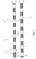
- Jeavon and his colleagues suggested to use a stack of perforated solid gamma converters combined with a multiwire proportional chamber.
- a large number of metal plates (copper) 12 are interleaved with Mylar sheets 14.
- the complete stack is perforated to form drift holes into which photoelectrons emitted from the copper plates 12 can be released. Secondary electrons resulting from gas ionization in the drift holes are extracted by an electric drift field and detected by a multiwire proportional chamber 16.
- the approach of combining gaseous detectors with solid converters has recently gained some new interest in the International Patent Application WO 01/59478 by Brahme et al. published on August 16, 2001 .
- the diagnostic and therapeutic detector system proposed by Brahme et al. is intended for imaging with both X-ray and gamma photons, and is based on a stack of well aligned, alternating perforated gamma converter layers 22 and gas electron multiplier layers (GEMs) 24, as schematically illustrated in Fig. 2 .
- the top layer in the alternating stack is preferably a GEM 24 for multiplication of electrons generated in the top gas volume.
- a sensor device 26 is arranged for collection of the electrons or photons resulting from the alternating converter and multiplier stack.
- the detector system of Brahme et al. constitutes a significant improvement, especially for gamma radiation, the X-ray efficiency and position resolution is still relatively poor due to the large mean free path of the converted electrons in the gas.
- the present invention overcomes these and other drawbacks of the prior art arrangements.
- Yet another object of the invention is to provide a radiation-based imaging system having an efficient radiation converter and radiation detector, especially for use in medical systems such as diagnostic and therapeutic systems for cancer treatment.
- the general idea according to the invention is to use a multi-layered converter, where each converter layer is adapted for interaction with incident radiation to cause the emission of electrons into drift holes defined in the converter layer, and the drift holes of one converter layer are staggered with respect to the drift holes of another converter layer.
- the effective conversion area will be increased, and the probability of incoming radiation passing through the stack without interaction with the converter layers will be significantly reduced. In this way, high absorption efficiency for incident radiation inside the multi-layered converter structure is ensured, while still maintaining transparency for emitted electrons through the drift holes.
- At least one of the converter layers comprises a columnar structure in order to increase the probability of electromagnetic interaction of the incident radiation.
- the columnar structure provides a large number of surface crossings of the incident radiation on its path through the structure, and thus results in efficient conversion of the incident radiation into electrons.
- the columnar structure is formed as a cesium iodide (CsI) layer.
- the converter layer may be provided with diamond, preferably CVD (Chemical Vapor Deposition) diamond, for improving the conversion efficiency of the incoming radiation into electrons.
- each converter layer comprises an upper electrode and lower electrode separated by an insulating material, with the drift holes being defined through the electrodes and the insulating material.
- the columnar structure mentioned above for example a columnar CsI layer, is preferably deposited on at least one of the electrodes and/or on the inner converter walls defining the drift holes.
- the incident radiation may be photons of various energies as well as charged and uncharged particles.
- the incoming radiation is in the form of photons, including X-rays and gamma radiation.
- the interaction mainly takes place in an effective zone adjacent to the inner dielectric walls of the drift holes.
- the staggered multi-layered converter architecture according to the invention increases the effective surface of these "edges" available for extraction of electrons into gas in the drift holes.
- the multi-layered converter stack according to the invention is preferably arranged in connection with a gaseous radiation detector, normally inside the gas chamber of the detector.
- the overall detector also comprises a sensor device sensitive to radiation representative of the electrons emitted from the converter layers, and arranged to provide an input to electronic signal processing means.
- the detector may be provided with a multiplication structure, preferably arranged in close vicinity above the sensor device, for avalanche multiplication of electrons and/or photo multiplication of photons to be detected by the sensor device.
- the radiation converter and detector according to the invention can be used in radiation-based imaging systems, for example in medical applications or for non-destructive testing.
- the multi-layered converter architecture according to the invention opens up for the possibility to convert radiation on very different energy levels in the same converter structure.
- the basic idea can be taken one step further by combining several individual converter stacks (oriented towards different energy intervals) in the same detector with a common sensor device.
- a first stack of mutually staggered converter layers adapted for photons of lower energy such as X-rays and a second stack of mutually staggered converter layers adapted for photons of higher energy such as gamma radiation in a radiation detector
- the same detector can be used for detection of both low and high energy photons. This is of particular interest in medical applications requiring both diagnostic imaging based on ordinary X-rays and portal imaging based on gamma radiation.
- the same detection unit can then be used for portal imaging based on the gamma beam.
- Fig. 3 is a schematic cross-sectional view of a converter stack according to a preferred embodiment of the invention.
- the converter stack 30 comprises two converter layers 32-1 and 32-2, each of which has a number of drift holes defined therein.
- Each converter layer preferably includes two electrode layers 34 separated by a support structure 35.
- the support structure 35 is normally made of an insulating material, and the electrode layers 34 may simply be a metallization on both sides of the insulating material.
- the converter layers 32-1 and 32-2 are preferably arranged in a conventional framework (not shown), possibly using dielectric spacers if required.
- the converter stack 30 generally has connection terminals for connecting the converter to an electric field generator for providing an electric drift field in a direction substantially parallel to the extension of the actual stack.
- each converter layer has connection terminals for connecting the electrodes 34 of the converter layer in question to respective potential sources (-V1, -V2; -V3, -V4), thus providing an electric drift field over the converter layer and in the drift holes. If
- the drift field may for example be generated by using the resistor chain arrangement described in the above-mentioned International Patent Application WO 01/59478 .
- the drift holes defined in the converter layer are preferably through-holes extending through the insulating material as well as the electrode metallization.
- Each converter layer is adapted to interact with incident radiation (indicated by solid curved lines), including photons and charged/uncharged particles, and more specifically X-rays and gamma radiation, to cause the emission of electrons (indicated by dashed curved lines) drifting into the drift holes.
- the effective conversion area will be increased, and the probability that incoming radiation will pass through the stack in the drift holes without interaction with the converter layers will be significantly reduced.
- the converter layers are thus mutually shifted with respect to each other along the extension of the converter layers themselves, or in other words in a direction substantially perpendicular to the extension of the actual converter stack.
- the shift distance d may of course vary from application to application, and is typically selected in dependence on the number of converter layers in the stack, as can be appreciated by comparing the converter stacks of Figs. 3 and 4 .
- the shift distance is often selected to maximize the overlap of the solid parts of the converter layers, thus minimizing the risk that incoming radiation passes through the stack inside the holes.
- the staggered converter architecture ensures full absorption of the X-rays inside the multi-layer structure.
- the released electrons can drift through the multi-layer structure almost freely due to the drift field in the drift holes and between the converter layers.
- the radiation converter is normally arranged in the gas chamber of a gaseous radiation detector. The drift through is additionally facilitated by the diffusion process in the gas gaps between the converter layers.
- a larger number of converter layers is normally used in the converter stack to ensure high absorption efficiency.
- converter layers have been illustrated as being composite with electrodes separated by an insulating support structure, it is actually possible, in a minimalistic implementation, to use a stack of mutually staggered perforated metallic plates and apply an electric drift field over the entire stack to obtain a reasonably efficient gamma converter.
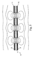
- Fig. 5 illustrates the dipole field in association with a single converter layer according to an embodiment of the invention.
- a potential difference (-V1, -V2) is applied between the electrodes 34 of a converter layer 32
- a dipole field will develop in the drift holes defined in the converter layer.
- the lines shown in Fig. 5 are equipotential lines, and thus the field lines are actually perpendicular to the illustrated lines. Electrons released into the gas will drift towards the high electric field region through the drift holes and focused therein.
- the converter layers are adapted for interaction with incident radiation to cause emission of electrons.
- the converter layers should be customized in accordance with the energy level of the incoming radiation.
- X-rays and radiation of similar energy it has turned out to be very beneficial to use a columnar structure on the converter layer to obtain efficient conversion of incident X-rays into electrons.
- the columnar structure is formed as a cesium iodide (CsI) layer, which is deposited on the converter layer at a suitable location.
- CsI cesium iodide
- Fig. 6 illustrates a first possible placement of the columnar structure for conversion of radiation of lower energy into electrons.
- the columnar structure 36 such as a columnar CsI layer, is deposited on the upper electrode metallization 34 of the converter layer 32.
- the incident X-ray (solid line) may cause the emission of several electrons (dashed lines) due to the larger number of surface crossings.
- the columnar structure 36 could equally well be deposited on the lower electrode metallization 34, or on both the upper and lower electrode metallization layers as illustrated in Fig. 7 .
- the columnar structure 36 may be deposited on the inner converter walls defining the drift holes, as illustrated in Fig. 8 .
- an efficient converter layer could be made of lead glass capillaries, possibly with slightly inclined capillaries, and with suitable metallization for providing the required electrodes.
- the interaction with incident gamma radiation to cause the emission of electrons into the drift holes mainly takes place in an effective zone in the insulating material adjacent to the inner walls of the drift holes, as illustrated in Fig. 9 .
- the staggered multi-layered converter architecture according to the invention thus increases the effective surface of these "edges" available for extraction of electrons into the gas in the drift holes.
- the converter layer may be provided with diamond (uniformly or non-uniformly) for improving the conversion efficiency of incoming radiation (especially applicable to X-rays) into electrons.
- diamond Chemical Vapor Deposition
- CVD Chemical Vapor Deposition
- CVD is generally a gas-phase chemical reaction occurring above a solid surface, causing deposition onto the surface.
- CVD techniques for producing diamond normally require some means of activating gas-phase carbon-containing precursor molecules, for example by maintaining the substrate within a given temperature interval and ensuring that the precursor gas is diluted in an excess of hydrogen.
- CVD diamond may be used as insulating material, for example sandwiched between two electrode layers.
- the CVD diamond may be deposited onto a first metal electrode layer, with a vacuum evaporated second metal layer on top of the CVD diamond.
- the use of CVD diamond is expected to give a very high yield ( ⁇ 20) of secondary electrons, thus resulting in a very efficient converter structure.
- the multi-layered converter architecture according to the invention makes it possible to convert radiation on very different energy levels in the same converter structure.
- the basic idea according to the invention can be taken one step further by arranging several individual converter stacks oriented towards different energy intervals in the same detector.
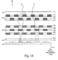
- Fig. 10 is a cross-sectional view of an example of a gaseous radiation detector according to a particular embodiment of the invention with two individual converter stacks oriented towards different energy intervals.
- the radiation detector 100 has a gas chamber in which the converter stacks 30-1, 30-2 are arranged.
- the gas chamber is filled with a suitable gas that can be selected from a broad spectrum of possible gases, including noble gases such as Xe, Ar, Kr and Ne, or gas mixtures like CO 2 or dimethylalcohol, as well as gas mixtures with quenching gases.
- a suitable gas including noble gases such as Xe, Ar, Kr and Ne, or gas mixtures like CO 2 or dimethylalcohol, as well as gas mixtures with quenching gases.
- the gas mixture may or may not be pressurized, and the gaseous detector may even be operated at sub-atmospheric pressure.
- the detector 100 has an inlet window 40 that is substantially transparent to the incoming radiation, including X-rays and gamma radiation.
- the detector 100 also comprises a sensor device 50 sensitive to radiation representative of the electrons emitted from the converter layers 30-1, 30-2, and arranged to provide an input to an electronic signal processing unit for signal processing such as signal amplification, A/D-conversion, digital filtering as well as image extraction and image processing.
- the same detector can thus be used for efficient detection of both low and high energy photons.
- the converter layers in the converter stack 30-1 adapted for X-rays are preferably provided with a columnar structure for efficient X-ray conversion.
- the number of converter layers in the two converter stacks 30-1, 30-2 may vary from application to application. For medical applications with X-ray imaging and portal imaging, a suitable number of converter layers in the X-ray stack may be 2-5 layers, whereas a suitable number of converter layers in the gamma stack may be 3-10 layers.
- a charge cloud drifts towards the anode, it normally induces a signal on a relatively large anode area (compared to the distance between the anode and the cathodes), resulting in smeared spatial resolution.
- a suitable multiplication structure 60 preferably arranged just above the sensor device 50, for avalanche multiplication of electrons and/or photo multiplication of photons to be detected by the sensor device.
- any conventional multiplier such as a parallel plate chamber, a multiwire proportional chamber or a gas electron multiplier, may be used.
- any conventional multiplier such as a parallel plate chamber, a multiwire proportional chamber or a gas electron multiplier
- the capillary structure preferably has relatively long capillaries with a capillary length that is many times larger than the capillary diameter.
- the electrons incident on the screen will induce emission of photons, which in turn may be detected by a photosensitive sensor device.
- the sensor device 50 also commonly referred to as a read-out plate, is thus generally provided as a charge collecting device or a photosensitive device, depending on whether electrons or photons are to be detected.
- the sensor device 50 may be a conventional multi-layer printed circuit board (PCB), with a number of charge collecting strips or pads distributed over the top surface of the board for providing position information.
- the multi-layer PCB has connections to read-out electronics, which in turn provide signal data to a signal-processing unit such as a computer.
- the position indicating pads or strips may be photosensitive elements, such as photo diodes, connected to the read-out electronics and the signal-processing unit.
- CCD Charge Couple Device
- the potential difference applied over an individual converter layer and between different layers depends on the thickness of the layers and the distance between the layers. For example, with a layer thickness in the order of 100 microns and an average distance between layers in the order of a few hundred microns, the potential difference over an individual layer could be a few 100 volts, and maybe slightly more between layers.
- Long track electrons which normally reduce the position resolution, may be electronically excluded from the final image, especially for lower dose rates when individual events may be resolved and selectively removed.
- the signal-processing electronics may then examine simultaneous signals from neighboring readout pads, and if more than a certain number of pads produce high signals, these signals are excluded so that the corresponding image information does not appear on the final image.
- Another way of reducing the contribution of long track electrons is to reduce the space between the converter layers, assuming that the majority of these electrons will be absorbed by the next converter layer before they drift sideways into a drift hole.
- the converter architecture according to the invention enables efficient detection of radiation with energies ranging from a few keV up to hundreds of MeV and higher, using one and the same detector unit.
- Fig. 11 shows a first radiation therapy set-up in which a radiation detector according to the invention may be implemented.
- the therapeutic and diagnostic machine 200 has a radiation head 210 including both a radiation source 212 for therapeutic irradiation and a diagnostic radiation source such as an X-ray tube 214.
- the diagnostic radiation source 212 may alternatively be arranged outside the radiation head 210.
- a patient 220 is positioned on a couch 230 and a radiation detector 100 according to the invention is placed underneath the patient for detection of both therapeutic radiation for portal imaging and diagnostic radiation for ordinary diagnostic imaging.
- the X-ray tube 214 in the radiation head 210 irradiates X-rays (typically 10-150 keV, and more preferably 60-100 keV) towards a specific area of interest in the patient 220.
- the X-rays are converted in the converter layers adapted for lower energy and the emitted electrons are then drifted towards the multiplication structure and finally detected by the sensor device in the radiation detector 100.
- radiation such as electrons or gamma radiation, of relatively high energy (typically 1-100 MeV, and more preferably 1-50 MeV) is collimated and irradiated from the radiation source 212 in the radiation head 210 towards a target volume 225 in the patient 220.
- the therapeutic radiation is converted in the converter layers adapted for higher energy and the emitted electrons are then drifted towards the multiplication structure and finally detected by the sensor device in the radiation detector.
- a computer (not illustrated) connected to the detector 100 provides images of the relevant parts of the patient, preferably illustrating the tumor and target volume.
- the diagnostic X-ray image which has relatively high quality and contrast, may be used for initial alignment of the patient on the couch to focus the radiation dose to the tumor, while minimizing the risk of exposing sensitive tissue and organs to the highly energetic therapy beams.
- the portal images obtained during the actual radiation treatment can be used as a complement to correct the patient set-up, and in principle enable on-line control and verification of the treatment.
- Fig. 12 shows a second radiation therapy set-up in which a radiation detector according to the invention may be implemented.
- the set-up of Fig. 12 is particularly adapted for accurate non-coplanar irradiation without involving movement of the patient, as well as for simplified automatic control of the movements of the gantry without risk for collisions with the patient.
- the basic design of the radiation machine 300 involves the arrangement of an inner gantry part 310 with two supporting locations relative to an outer gantry part 320, with the two supporting locations being placed at each side of the treatment volume of the patient.
- the inner gantry part 310 comprises in the present embodiment a circular arc portion 313, a first ring portion 314 and a second ring portion 315.
- a radiation head 210 is mechanically supported by the inner gantry part 301, movable along the arc portion 313 from the first ring portion 314 to the second 315 ring portion.
- the patient 220 is placed on a couch 230, and a treatment radiation source 212 in the radiation head 210 is arranged to direct a treatment beam or dose package to a target volume 225 in the patient 220.
- the ring portions 314, 315 of the inner gantry part 310 are situated on either side of the target volume 225.
- the ring portions 314, 315 are rotatably supported by the outer gantry part 320, comprising a first support portion 326 and a second support portion 327.
- This design guarantees that the center of mass of the inner gantry part 310 always is situated between the support locations and therefore a relative low bending moment is present in the gantry.
- This stable arrangement makes it possible to rotate the inner gantry part 310 relative the outer gantry part 320 around a substantially horizontal rotation axis 340.
- the treatment volume 225 is preferably positioned at this rotation axis 340.
- the treatment radiation source 212 may irradiate the treatment volume 225 from above, below and from either side thereof.
- the arc portion 313 and the movable radiation head 210 makes it possible to achieve accurate non-coplanar treatment. By combing the movement of the head 210 along the arc 313 with the rotation of the inner gantry portion 310 around the patient 220, a multitude of irradiation directions is obtained.
- a diagnostic radiation source 214 such as an X-ray tube in the inner gantry part 310, preferably in the radiation head 210, and providing the radiation machine 300 with a radiation detector 100 according to the invention
- a complete radiation-based imaging system for diagnostic as well as portal imaging is obtained.
- the X-ray tube 214 is operated and the detector 100 with its associated electronic equipment and signal-processing unit provides an X-ray image of the treatment volume that can be used for the initial patient alignment.
- the radiation beams passes through the patient 220, preferably through the target volume 225, and are subsequently detected by the detector 100.
- the detector 100 is preferably supported on the inner gantry part 310.
- images from several different directions around the target volume 225 can be taken.
- processing these images using suitable commercially available software a 3-dimensional CT scan like representation of the patient with the tumor and adjacent tissues, organs and bones may be obtained.
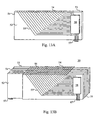
- Fig. 13A is a schematic diagram illustrating a printed circuit board according to a preferred embodiment of the invention, with sensor cells arranged along the edge of the board and where the depth of the board is used for connection lines to outside circuitry.
- the circuit board 51 is defined by two main surfaces 52 and four edge surfaces 53.
- a row of radiation sensitive elements 54 is arranged at one of the edge surfaces.
- connection lines 55 lead from each radiation sensitive element 54 to signal processing means 58, such as an ASIC, preferably without any wire-crossings.
- the signal processing means 58 is preferably located at the same board 51 as addressed radiation sensitive elements 64 but at a distance therefrom to avoid radiation damages on the sensitive electronics.
- Read-out connections 57 are provided at the signal processing means 58 to connect the circuit board 51 to external processing means.
- a radiation sensor 50 is obtained, as is illustrated in Fig. 13B .
- the boards 51 are preferably placed in a support structure (not illustrated), facilitating removal/insertion of individual boards 51.
- the boards could also be adhesively attached to each other, e.g. by means of glue, or still differently arranged.
- a sensor surface 56 is formed by the rows of radiation sensitive elements 54.
- the signal processing means 58 generally protrudes above the main surface 52 of each circuit board 51 and is in a preferred embodiment placed at an end portion of the respective circuit board 51.
- a compact sensor 50 is formed.
- Another embodiment achieves a similar advantageous space utilization by arranging the signal processing means of adjacent boards in a non-overlapping way at different heights, instead of at different board ends.
- the area of the formed sensor surface 56 is preferably in the order of dm 3 , with the total number of sensitive elements in the order of hundred thousand.
- the radiation sensitive elements 54 may be charge collectors, radiation sensitive diodes, e.g. photodiodes, or any other element capable of sensing the radiation reaching the sensor surface.
- Incident electrons are preferably sensed by pixels made of thin film of a conducting material, e.g. copper.
- the copper islands can reside charge of the surrounding radiation, which may be collected via the signal processing means 58 at predefined points of time.
- the main body of the circuit board 51 is preferably composed of a non-conducting material, such as a polymer material.
- the connection lines 55 between the individual radiation sensitive elements 54 and signal processing means 58 are for example realized as metal wires. It is desirable to implement a line pattern that uses the main surface 52 of the board 51 as efficiently as possible, preferably without unnecessary crossings.
- each circuit board is defined by two main surfaces and at least one edge surface, where the area of the edge surface typically is substantially smaller than the area of the main surfaces.
- the radiation sensitive elements arranged on the respective circuit board are preferably placed such that, in operation, the edge surface and an active surface of each of the radiation sensitive elements are facing the incident radiation.
- the radiation sensitive elements are arranged at or in the vicinity of at least one edge surface of the respective circuit board.
- detector structures including an amorphous silicon flat-panel detector, preferably adapted for both high and low energy radiation, i.e. treatment and diagnostic radiation, respectively.
Landscapes
- Physics & Mathematics (AREA)
- Health & Medical Sciences (AREA)
- Life Sciences & Earth Sciences (AREA)
- General Physics & Mathematics (AREA)
- High Energy & Nuclear Physics (AREA)
- Molecular Biology (AREA)
- Spectroscopy & Molecular Physics (AREA)
- Measurement Of Radiation (AREA)
- Production Of Multi-Layered Print Wiring Board (AREA)
- Coils Or Transformers For Communication (AREA)
- Particle Accelerators (AREA)
- Light Receiving Elements (AREA)
Abstract
Description
- The present invention generally concerns radiation converters and radiation detectors, and more particularly the use of such converters and detectors in radiation-based imaging systems for applications such as medical imaging and non-destructive testing.
- Radiation detectors are used for detection of incoming radiation such as X-rays, gamma photons and charged/uncharged particles, in a wide range of different applications. For detection of photons of various energies, the incoming photons are converted to electrons through electromagnetic interactions, including the photoelectric effect, pair production and the Compton effect. The emitted electrons are normally multiplied by a multiplication structure to produce a multiplicity of secondary electrons and/or photons, which in turn may be detected by a suitable sensor device.
- For low-energy photons, gas conversion is very successful with almost 100% efficiency combined with high spatial resolution. However, as the photon energy increases, gas conversion becomes less attractive since the photoelectric capture cross section falls rapidly and the photoelectron range increases. This results in degraded efficiency, as well as heavily deteriorated spatial resolution due to the extended tracks of the long-range electrons.
- For higher photon energies, a successful approach is to provide gaseous radiation detectors with a solid converter to increase the probability of electromagnetic interaction with the incoming radiation. Such a converter is needed in order to increase the efficiency since higher energy photons are much more penetrating and would otherwise pass the detector undetected. Compared to non-gaseous detectors, there are several advantages of such an approach, including improved efficiency, low price and larger sensitive area. These advantages have stimulated many researchers to develop gaseous detectors combined with solid converters.
- Probably one of the first attempts to combine gaseous detectors and solid converters was made by Jeavon et al, as described in the article The High-Density Multiwire Drift Chamber, Nuclear Instruments and Methods, 124, 1975, pp. 491-503. Jeavon and his colleagues suggested to use a stack of perforated solid gamma converters combined with a multiwire proportional chamber. As illustrated in
Fig. 1 , a large number of metal plates (copper) 12 are interleaved with Mylarsheets 14. The complete stack is perforated to form drift holes into which photoelectrons emitted from thecopper plates 12 can be released. Secondary electrons resulting from gas ionization in the drift holes are extracted by an electric drift field and detected by a multiwireproportional chamber 16. - In the article High resistance Lead Glass Tubing for Rich Counters and for Electromagnetic Calorimeters in Nuclear Instruments and Methods in Physics Research, A257, 1987, pp. 609-613, Del Guerra et al. suggested to use an array of lead glass tubing combined with a multiwire proportional chamber. The lead glass tubing acts as a combined gamma converter and electron drift structure, with the possibility of gas multiplication inside the lead glass capillaries.
- However, both of these developments have not received any wide spread use due to the fact that the efficiency of the converters is still relatively low (a few %). The low efficiency is associated with the fact that electrons created by gamma radiation inside the converters have a very short mean free path (normally less than a fraction of a mm). As a result, only electrons created in the converters near the inner walls to the holes or capillaries can penetrate freely into the gas volume.
- There have also been attempts to develop gaseous detectors with X-ray converters. As described in
U.S. Patent 5,192,861 issued to Breskin et al. on March 9, 1993 , a thin flat cesium iodide (CsI) layer was used as a converter. However, the efficiency of the CsI converter layer is also very low for the same reason as mentioned above. In addition, the useful surface of the converter is actually rather small due to the acute angle necessary to obtain a reasonable efficiency. As a result, this type of detector has not gained any practical application. - The approach of combining gaseous detectors with solid converters has recently gained some new interest in the International Patent Application
WO 01/59478 by Brahme et al. published on August 16, 2001 gamma converter layers 22 and gas electron multiplier layers (GEMs) 24, as schematically illustrated inFig. 2 . The top layer in the alternating stack is preferably aGEM 24 for multiplication of electrons generated in the top gas volume. In the gas volume between the inlet window and the top GEM, diagnostic X-rays will interact with the gas and emit electrons, which are collected and amplified by theGEM structures 24 in the stack. For photons in the radiation therapy beam, the top gas volume will be more or less transparent, and such higher energy photons penetrates into the stack and converts into electrons in thedifferent converter layers 22. High-energy photons of relatively lower energy will predominantly convert in the top converter layers, while photons of relatively higher energy will dominate in the bottom layers. At the bottom, asensor device 26 is arranged for collection of the electrons or photons resulting from the alternating converter and multiplier stack. - Although the detector system of Brahme et al. constitutes a significant improvement, especially for gamma radiation, the X-ray efficiency and position resolution is still relatively poor due to the large mean free path of the converted electrons in the gas.
- Various other attempts to improve the X-ray efficiency in gaseous radiation detectors include using inclined capillaries, as described in
U.S. Patent 6,333,506 issued to Francke et al. on December 25, 2001 . - The present invention overcomes these and other drawbacks of the prior art arrangements.
- It is a general object of the present invention to improve upon existing solutions to the combined problem of providing high efficiency and high spatial resolution in radiation detectors.
- It is an object of the invention to provide an efficient, accurate and reliable radiation converter.
- It is also an object of the invention to provide an efficient radiation detector, especially one that allows detection of photons in a broad energy range, including both low energy photons and high-energy photons.
- Yet another object of the invention is to provide a radiation-based imaging system having an efficient radiation converter and radiation detector, especially for use in medical systems such as diagnostic and therapeutic systems for cancer treatment.
- These and other objects are met by the invention as defined by the accompanying patent claims.
- The general idea according to the invention is to use a multi-layered converter, where each converter layer is adapted for interaction with incident radiation to cause the emission of electrons into drift holes defined in the converter layer, and the drift holes of one converter layer are staggered with respect to the drift holes of another converter layer. By mutually shifting the converter layers such that the drift holes of two different layers are no longer well-aligned, but rather staggered with respect to each other, the effective conversion area will be increased, and the probability of incoming radiation passing through the stack without interaction with the converter layers will be significantly reduced. In this way, high absorption efficiency for incident radiation inside the multi-layered converter structure is ensured, while still maintaining transparency for emitted electrons through the drift holes.
- For X-rays, at least one of the converter layers comprises a columnar structure in order to increase the probability of electromagnetic interaction of the incident radiation. The columnar structure provides a large number of surface crossings of the incident radiation on its path through the structure, and thus results in efficient conversion of the incident radiation into electrons. Preferably, the columnar structure is formed as a cesium iodide (CsI) layer. Alternatively, the converter layer may be provided with diamond, preferably CVD (Chemical Vapor Deposition) diamond, for improving the conversion efficiency of the incoming radiation into electrons.
- Normally, each converter layer comprises an upper electrode and lower electrode separated by an insulating material, with the drift holes being defined through the electrodes and the insulating material. The columnar structure mentioned above, for example a columnar CsI layer, is preferably deposited on at least one of the electrodes and/or on the inner converter walls defining the drift holes.
- In general, the incident radiation may be photons of various energies as well as charged and uncharged particles. In the preferred applications, the incoming radiation is in the form of photons, including X-rays and gamma radiation.
- For gamma radiation, the interaction mainly takes place in an effective zone adjacent to the inner dielectric walls of the drift holes. The staggered multi-layered converter architecture according to the invention increases the effective surface of these "edges" available for extraction of electrons into gas in the drift holes.
- The multi-layered converter stack according to the invention is preferably arranged in connection with a gaseous radiation detector, normally inside the gas chamber of the detector. The overall detector also comprises a sensor device sensitive to radiation representative of the electrons emitted from the converter layers, and arranged to provide an input to electronic signal processing means. For improved performance, the detector may be provided with a multiplication structure, preferably arranged in close vicinity above the sensor device, for avalanche multiplication of electrons and/or photo multiplication of photons to be detected by the sensor device.
- The radiation converter and detector according to the invention can be used in radiation-based imaging systems, for example in medical applications or for non-destructive testing.
- As indicated above, the multi-layered converter architecture according to the invention opens up for the possibility to convert radiation on very different energy levels in the same converter structure. The basic idea can be taken one step further by combining several individual converter stacks (oriented towards different energy intervals) in the same detector with a common sensor device. By arranging a first stack of mutually staggered converter layers adapted for photons of lower energy such as X-rays, and a second stack of mutually staggered converter layers adapted for photons of higher energy such as gamma radiation in a radiation detector, the same detector can be used for detection of both low and high energy photons. This is of particular interest in medical applications requiring both diagnostic imaging based on ordinary X-rays and portal imaging based on gamma radiation. In cancer treatment for example, this means that it may be possible to obtain a high quality medical X-ray image at the therapy site directly before therapeutic irradiation begins, without the need for replacement of the detection unit. During the subsequent irradiation therapy, the same detection unit can then be used for portal imaging based on the gamma beam.
- Other advantages offered by the present invention will be appreciated upon reading of the below description of the embodiments of the invention.
- The invention, together with further objects and advantages thereof, will be best understood by reference to the following description taken together with the accompanying drawings, in which:
-
Fig. 1 illustrates a stack of perforated solid gamma converters combined with a multiwire proportional chamber according to the prior art; -
Fig. 2 illustrates a stack of well aligned, alternating perforated gamma converter layers and gas electron multiplier layers according to the prior art; -
Fig. 3 is a schematic cross-sectional view of a converter stack according to a preferred embodiment of the invention; -
Fig. 4 is a schematic cross-sectional view of a converter stack according to another preferred embodiment of the invention; -
Fig. 5 illustrates the dipole field in association with a single converter layer according to an embodiment of the invention; -
Fig. 6 illustrates a first possible placement of the columnar structure for conversion of radiation of lower energy into electrons; -
Fig. 7 illustrates a second possible placement of the columnar structure for conversion of radiation of lower energy into electrons; -
Fig. 8 illustrates a third possible placement of the columnar structure for conversion of radiation of lower energy into electrons; -
Fig. 9 illustrates the efficient gamma conversion zone in the dielectric converter material; -
Fig. 10 is a cross-sectional view of an example of a gaseous radiation detector according to a particular embodiment of the invention with two individual converter stacks oriented towards different energy intervals; -
Fig. 11 shows a first radiation therapy set-up in which a radiation detector according to the invention may be implemented; -
Fig. 12 shows a second radiation therapy set-up in which a radiation detector according to the invention may be implemented; -
Fig. 13A is a schematic diagram illustrating a printed circuit board according to a preferred embodiment of the invention, with sensor cells arranged along the edge of the board and where the depth of the board is used for connection lines to outside circuitry; -
Fig. 13B is a schematic diagram illustrating a radiation sensor device formed by arranging several printed circuit boards of the type shown inFig. 13A adjacent to each other. - Throughout the drawings, the same reference characters will be used for corresponding or similar elements.
-
Fig. 3 is a schematic cross-sectional view of a converter stack according to a preferred embodiment of the invention. In this particular example, theconverter stack 30 comprises two converter layers 32-1 and 32-2, each of which has a number of drift holes defined therein. Each converter layer preferably includes twoelectrode layers 34 separated by asupport structure 35. Thesupport structure 35 is normally made of an insulating material, and the electrode layers 34 may simply be a metallization on both sides of the insulating material. The converter layers 32-1 and 32-2 are preferably arranged in a conventional framework (not shown), possibly using dielectric spacers if required. - The
converter stack 30 generally has connection terminals for connecting the converter to an electric field generator for providing an electric drift field in a direction substantially parallel to the extension of the actual stack. Typically, each converter layer has connection terminals for connecting theelectrodes 34 of the converter layer in question to respective potential sources (-V1, -V2; -V3, -V4), thus providing an electric drift field over the converter layer and in the drift holes. If |V1|>|V2|>|V3|>|V4|, there will also be an electric field between the different converter layers. The drift field may for example be generated by using the resistor chain arrangement described in the above-mentioned International Patent ApplicationWO 01/59478 - The drift holes defined in the converter layer are preferably through-holes extending through the insulating material as well as the electrode metallization. Each converter layer is adapted to interact with incident radiation (indicated by solid curved lines), including photons and charged/uncharged particles, and more specifically X-rays and gamma radiation, to cause the emission of electrons (indicated by dashed curved lines) drifting into the drift holes.
- By mutually shifting the converter layers such that the drift holes of the two different layers 32-1 and 32-2 are no longer well-aligned, but rather staggered with respect to each other, the effective conversion area will be increased, and the probability that incoming radiation will pass through the stack in the drift holes without interaction with the converter layers will be significantly reduced. The converter layers are thus mutually shifted with respect to each other along the extension of the converter layers themselves, or in other words in a direction substantially perpendicular to the extension of the actual converter stack. The shift distance d may of course vary from application to application, and is typically selected in dependence on the number of converter layers in the stack, as can be appreciated by comparing the converter stacks of
Figs. 3 and4 . The shift distance is often selected to maximize the overlap of the solid parts of the converter layers, thus minimizing the risk that incoming radiation passes through the stack inside the holes. For photons of relatively lower energy, such as X-rays, the staggered converter architecture ensures full absorption of the X-rays inside the multi-layer structure. At the same time, the released electrons can drift through the multi-layer structure almost freely due to the drift field in the drift holes and between the converter layers. The radiation converter is normally arranged in the gas chamber of a gaseous radiation detector. The drift through is additionally facilitated by the diffusion process in the gas gaps between the converter layers. For photons of relatively higher energy, such as gamma radiation, a larger number of converter layers is normally used in the converter stack to ensure high absorption efficiency. - Although the converter layers have been illustrated as being composite with electrodes separated by an insulating support structure, it is actually possible, in a minimalistic implementation, to use a stack of mutually staggered perforated metallic plates and apply an electric drift field over the entire stack to obtain a reasonably efficient gamma converter.
-
Fig. 5 illustrates the dipole field in association with a single converter layer according to an embodiment of the invention. When a potential difference (-V1, -V2) is applied between theelectrodes 34 of aconverter layer 32, a dipole field will develop in the drift holes defined in the converter layer. The lines shown inFig. 5 are equipotential lines, and thus the field lines are actually perpendicular to the illustrated lines. Electrons released into the gas will drift towards the high electric field region through the drift holes and focused therein. If desired, it is also possible to explore the gas multiplication process inside the converter layers and/or in the gas gap between them by increasing the potential difference over the converter layers and/or between the layers. It must though be pointed out that gas multiplication inside the converter layers is not a necessary feature. It is clearly sufficient to select a potential difference over the converter layer so as to ensure an efficient drift field. - As indicated above, the converter layers are adapted for interaction with incident radiation to cause emission of electrons. For optimal performance, the converter layers should be customized in accordance with the energy level of the incoming radiation. For X-rays and radiation of similar energy, it has turned out to be very beneficial to use a columnar structure on the converter layer to obtain efficient conversion of incident X-rays into electrons.
- By using a columnar structure with multiple columns extending from the converter layer, the probability of electromagnetic interaction of the incident radiation increases since the columns provides a large number of surface crossings of the incident radiation on its path through the structure. This results in efficient conversion of the incident radiation into electrons, and may also give a slight electron multiplication effect as an inherent property of the columnar structure. Preferably, the columnar structure is formed as a cesium iodide (CsI) layer, which is deposited on the converter layer at a suitable location.
-
Fig. 6 illustrates a first possible placement of the columnar structure for conversion of radiation of lower energy into electrons. In this example, thecolumnar structure 36, such as a columnar CsI layer, is deposited on theupper electrode metallization 34 of theconverter layer 32. As schematically illustrated inFig. 6 , the incident X-ray (solid line) may cause the emission of several electrons (dashed lines) due to the larger number of surface crossings. Thecolumnar structure 36 could equally well be deposited on thelower electrode metallization 34, or on both the upper and lower electrode metallization layers as illustrated inFig. 7 . Alternatively, or in combination with any of the previous locations, thecolumnar structure 36 may be deposited on the inner converter walls defining the drift holes, as illustrated inFig. 8 . - For more information on columnar CsI layers, reference is made to the articles Moisture Proof Columnar Cesium Iodide (CsI) Layers for Gas Avalanche Microdetectors by Park et al., IEEE Transactions on Nuclear Science, Vol. 46, No. 6, December 1999, pp. 1938-1942 and A Columnar Cesium Iodide (CsI) Drift Plane Layer for Gas Avalanche Microdetectors by Cho et al., IEEE Transactions on Nuclear Science, Vol. 45, No. 3, June 1998, pp. 275-279. Park and Cho with colleagues suggested to use a columnar CsI drift plane layer as an efficient secondary electron emitter, placing a thin columnar CsI layer on top of the drift plane with Kapton® spacers between the drift layer and the CsI layer.
- For gamma radiation, an efficient converter layer could be made of lead glass capillaries, possibly with slightly inclined capillaries, and with suitable metallization for providing the required electrodes. The interaction with incident gamma radiation to cause the emission of electrons into the drift holes mainly takes place in an effective zone in the insulating material adjacent to the inner walls of the drift holes, as illustrated in
Fig. 9 . The staggered multi-layered converter architecture according to the invention thus increases the effective surface of these "edges" available for extraction of electrons into the gas in the drift holes. - The converter layer (or layers) may be provided with diamond (uniformly or non-uniformly) for improving the conversion efficiency of incoming radiation (especially applicable to X-rays) into electrons. Preferably, CVD (Chemical Vapor Deposition) techniques are used for causing diamond deposition, for example vaporized from methane (CH4) gas. CVD is generally a gas-phase chemical reaction occurring above a solid surface, causing deposition onto the surface. CVD techniques for producing diamond normally require some means of activating gas-phase carbon-containing precursor molecules, for example by maintaining the substrate within a given temperature interval and ensuring that the precursor gas is diluted in an excess of hydrogen.
- In the converter layers, CVD diamond may be used as insulating material, for example sandwiched between two electrode layers. For manufacturing, the CVD diamond may be deposited onto a first metal electrode layer, with a vacuum evaporated second metal layer on top of the CVD diamond. Alternatively, it is possible to provide the CVD diamond as a diamond film or coating on one or both of the electrodes and/or on the walls defining the capillary holes. The use of CVD diamond is expected to give a very high yield (~20) of secondary electrons, thus resulting in a very efficient converter structure.
- The multi-layered converter architecture according to the invention makes it possible to convert radiation on very different energy levels in the same converter structure. The basic idea according to the invention can be taken one step further by arranging several individual converter stacks oriented towards different energy intervals in the same detector.
-
Fig. 10 is a cross-sectional view of an example of a gaseous radiation detector according to a particular embodiment of the invention with two individual converter stacks oriented towards different energy intervals. - The
radiation detector 100 has a gas chamber in which the converter stacks 30-1, 30-2 are arranged. In operation, the gas chamber is filled with a suitable gas that can be selected from a broad spectrum of possible gases, including noble gases such as Xe, Ar, Kr and Ne, or gas mixtures like CO2 or dimethylalcohol, as well as gas mixtures with quenching gases. The gas mixture may or may not be pressurized, and the gaseous detector may even be operated at sub-atmospheric pressure. - The
detector 100 has aninlet window 40 that is substantially transparent to the incoming radiation, including X-rays and gamma radiation. Thedetector 100 also comprises asensor device 50 sensitive to radiation representative of the electrons emitted from the converter layers 30-1, 30-2, and arranged to provide an input to an electronic signal processing unit for signal processing such as signal amplification, A/D-conversion, digital filtering as well as image extraction and image processing. - By arranging a first stack 30-1 of mutually staggered converter layers adapted for photons of lower energy such as X-rays, and a second stack 30-2 of mutually staggered converter layers adapted for photons of higher energy such as gamma radiation inside the gas chamber, the same detector can thus be used for efficient detection of both low and high energy photons. The converter layers in the converter stack 30-1 adapted for X-rays are preferably provided with a columnar structure for efficient X-ray conversion. The number of converter layers in the two converter stacks 30-1, 30-2 may vary from application to application. For medical applications with X-ray imaging and portal imaging, a suitable number of converter layers in the X-ray stack may be 2-5 layers, whereas a suitable number of converter layers in the gamma stack may be 3-10 layers.
- When a charge cloud drifts towards the anode, it normally induces a signal on a relatively large anode area (compared to the distance between the anode and the cathodes), resulting in smeared spatial resolution. However, by multiplying the drifting charge, for example by avalanche multiplication, near the anode the effect of the induced charge on the spatial resolution will be negligible compared to the multiplied real charge cloud. Consequently, it is beneficial to use a suitable multiplication structure 60, preferably arranged just above the
sensor device 50, for avalanche multiplication of electrons and/or photo multiplication of photons to be detected by the sensor device. - For electron multiplication, any conventional multiplier such as a parallel plate chamber, a multiwire proportional chamber or a gas electron multiplier, may be used. For photo multiplication, it is possible to use any of the above conventional electron multipliers since an ordinary electron avalanche also produces a great number of photons. However, it may be recommendable to use a long capillary hole type multiplier, such as a lead glass capillary structure, operated at a potential difference sufficient for photo multiplication, but still below the threshold for electron multiplication. For efficient photo multiplication, the capillary structure preferably has relatively long capillaries with a capillary length that is many times larger than the capillary diameter.
- It is also possible to convert the electron avalanche produced by an electron multiplier into photons by using a fluorescent screen at the bottom of the detector. The electrons incident on the screen will induce emission of photons, which in turn may be detected by a photosensitive sensor device.
- The
sensor device 50, also commonly referred to as a read-out plate, is thus generally provided as a charge collecting device or a photosensitive device, depending on whether electrons or photons are to be detected. For example, thesensor device 50 may be a conventional multi-layer printed circuit board (PCB), with a number of charge collecting strips or pads distributed over the top surface of the board for providing position information. The multi-layer PCB has connections to read-out electronics, which in turn provide signal data to a signal-processing unit such as a computer. In the case of a photosensitive sensor device, the position indicating pads or strips may be photosensitive elements, such as photo diodes, connected to the read-out electronics and the signal-processing unit. It is also possible to use conventional CCD (Charge Couple Device) technology, including suitable optics for guiding the photons to the CCD sensor. In applications using high energy irradiation, it should be understood that the detectors need to be highly radiation tolerant, and this has to be taken into account in the design of the detector in general and the sensor device with associated read-out electronics in particular. - The potential difference applied over an individual converter layer and between different layers depends on the thickness of the layers and the distance between the layers. For example, with a layer thickness in the order of 100 microns and an average distance between layers in the order of a few hundred microns, the potential difference over an individual layer could be a few 100 volts, and maybe slightly more between layers. Using the notation of
Fig. 10 , |V1|>|V2|>|V3|> ... >|V13|. - Long track electrons, which normally reduce the position resolution, may be electronically excluded from the final image, especially for lower dose rates when individual events may be resolved and selectively removed. The signal-processing electronics may then examine simultaneous signals from neighboring readout pads, and if more than a certain number of pads produce high signals, these signals are excluded so that the corresponding image information does not appear on the final image.
- Another way of reducing the contribution of long track electrons is to reduce the space between the converter layers, assuming that the majority of these electrons will be absorbed by the next converter layer before they drift sideways into a drift hole.
- A new type of sensor device that can be used by the invention will be described later on with reference to
Figs. 13A-B . - The converter architecture according to the invention enables efficient detection of radiation with energies ranging from a few keV up to hundreds of MeV and higher, using one and the same detector unit.
- This is of particular interest in medical applications requiring both diagnostic imaging based on ordinary X-rays and portal imaging based on gamma radiation. In cancer treatment for example, this means that it is possible to obtain a high quality medical X-ray image at the therapy site directly before therapeutic irradiation begins, without the need for replacement of the detection unit. During the subsequent irradiation therapy, the same detection unit can then be used for portal imaging based on the gamma beam.
-
Fig. 11 shows a first radiation therapy set-up in which a radiation detector according to the invention may be implemented. In this particular embodiment, the therapeutic anddiagnostic machine 200 has aradiation head 210 including both aradiation source 212 for therapeutic irradiation and a diagnostic radiation source such as anX-ray tube 214. Naturally, thediagnostic radiation source 212 may alternatively be arranged outside theradiation head 210. Apatient 220 is positioned on acouch 230 and aradiation detector 100 according to the invention is placed underneath the patient for detection of both therapeutic radiation for portal imaging and diagnostic radiation for ordinary diagnostic imaging. For diagnostic purposes, theX-ray tube 214 in theradiation head 210 irradiates X-rays (typically 10-150 keV, and more preferably 60-100 keV) towards a specific area of interest in thepatient 220. The X-rays are converted in the converter layers adapted for lower energy and the emitted electrons are then drifted towards the multiplication structure and finally detected by the sensor device in theradiation detector 100. During therapy, radiation, such as electrons or gamma radiation, of relatively high energy (typically 1-100 MeV, and more preferably 1-50 MeV) is collimated and irradiated from theradiation source 212 in theradiation head 210 towards atarget volume 225 in thepatient 220. The therapeutic radiation is converted in the converter layers adapted for higher energy and the emitted electrons are then drifted towards the multiplication structure and finally detected by the sensor device in the radiation detector. - Based on the radiation detected by the sensor device, a computer (not illustrated) connected to the
detector 100 provides images of the relevant parts of the patient, preferably illustrating the tumor and target volume. The diagnostic X-ray image, which has relatively high quality and contrast, may be used for initial alignment of the patient on the couch to focus the radiation dose to the tumor, while minimizing the risk of exposing sensitive tissue and organs to the highly energetic therapy beams. The portal images obtained during the actual radiation treatment can be used as a complement to correct the patient set-up, and in principle enable on-line control and verification of the treatment. -
Fig. 12 shows a second radiation therapy set-up in which a radiation detector according to the invention may be implemented. The set-up ofFig. 12 is particularly adapted for accurate non-coplanar irradiation without involving movement of the patient, as well as for simplified automatic control of the movements of the gantry without risk for collisions with the patient. The basic design of theradiation machine 300 involves the arrangement of aninner gantry part 310 with two supporting locations relative to anouter gantry part 320, with the two supporting locations being placed at each side of the treatment volume of the patient. Theinner gantry part 310 comprises in the present embodiment acircular arc portion 313, afirst ring portion 314 and asecond ring portion 315. Aradiation head 210 is mechanically supported by the inner gantry part 301, movable along thearc portion 313 from thefirst ring portion 314 to the second 315 ring portion. Thepatient 220 is placed on acouch 230, and atreatment radiation source 212 in theradiation head 210 is arranged to direct a treatment beam or dose package to atarget volume 225 in thepatient 220. In this particular example, thering portions inner gantry part 310 are situated on either side of thetarget volume 225. Thering portions outer gantry part 320, comprising afirst support portion 326 and asecond support portion 327. This design, guarantees that the center of mass of theinner gantry part 310 always is situated between the support locations and therefore a relative low bending moment is present in the gantry. This stable arrangement makes it possible to rotate theinner gantry part 310 relative theouter gantry part 320 around a substantiallyhorizontal rotation axis 340. - The
treatment volume 225 is preferably positioned at thisrotation axis 340. Thus, since theinner gantry part 310 is rotatable around therotation axis 340, thetreatment radiation source 212 may irradiate thetreatment volume 225 from above, below and from either side thereof. In addition, thearc portion 313 and themovable radiation head 210 makes it possible to achieve accurate non-coplanar treatment. By combing the movement of thehead 210 along thearc 313 with the rotation of theinner gantry portion 310 around thepatient 220, a multitude of irradiation directions is obtained. - By arranging a
diagnostic radiation source 214 such as an X-ray tube in theinner gantry part 310, preferably in theradiation head 210, and providing theradiation machine 300 with aradiation detector 100 according to the invention, a complete radiation-based imaging system for diagnostic as well as portal imaging is obtained. For diagnostic imaging, theX-ray tube 214 is operated and thedetector 100 with its associated electronic equipment and signal-processing unit provides an X-ray image of the treatment volume that can be used for the initial patient alignment. During radiation therapy, the radiation beams passes through thepatient 220, preferably through thetarget volume 225, and are subsequently detected by thedetector 100. - The
detector 100 is preferably supported on theinner gantry part 310. By rotating theinner gantry part 310 around therotation axis 340 and continuously or intermittently irradiating thepatient 220 with theX-ray tube 214, images from several different directions around thetarget volume 225 can be taken. By processing these images using suitable commercially available software, a 3-dimensional CT scan like representation of the patient with the tumor and adjacent tissues, organs and bones may be obtained. -
Fig. 13A is a schematic diagram illustrating a printed circuit board according to a preferred embodiment of the invention, with sensor cells arranged along the edge of the board and where the depth of the board is used for connection lines to outside circuitry. Thecircuit board 51 is defined by two main surfaces 52 and four edge surfaces 53. A row of radiationsensitive elements 54 is arranged at one of the edge surfaces. Typically,connection lines 55 lead from each radiationsensitive element 54 to signal processing means 58, such as an ASIC, preferably without any wire-crossings. The signal processing means 58 is preferably located at thesame board 51 as addressed radiation sensitive elements 64 but at a distance therefrom to avoid radiation damages on the sensitive electronics. Read-outconnections 57 are provided at the signal processing means 58 to connect thecircuit board 51 to external processing means. Thus, with the circuit board design ofFig. 13A , a small surface at the edge portion of thecircuit board 51 is used as an area for radiation sensing, whereas the larger main surface 52 is used for the space-demanding wiring and electronics. - By arranging a number of
circuit boards 51 ofFig. 13A adjacent to each other, aradiation sensor 50 is obtained, as is illustrated inFig. 13B . Theboards 51 are preferably placed in a support structure (not illustrated), facilitating removal/insertion ofindividual boards 51. The boards could also be adhesively attached to each other, e.g. by means of glue, or still differently arranged. In such a way, asensor surface 56 is formed by the rows of radiationsensitive elements 54. The signal processing means 58 generally protrudes above the main surface 52 of eachcircuit board 51 and is in a preferred embodiment placed at an end portion of therespective circuit board 51. By arranging thecircuit boards 51 such that adjacent boards have their signal processing means 58 at opposite ends, as illustrated inFig. 13B , and restricting the maximum allowed protrusion of the signal processing means 58 to one circuit board thickness, acompact sensor 50 is formed. Another embodiment achieves a similar advantageous space utilization by arranging the signal processing means of adjacent boards in a non-overlapping way at different heights, instead of at different board ends. The area of the formedsensor surface 56 is preferably in the order of dm3, with the total number of sensitive elements in the order of hundred thousand. - The radiation
sensitive elements 54 may be charge collectors, radiation sensitive diodes, e.g. photodiodes, or any other element capable of sensing the radiation reaching the sensor surface. Incident electrons are preferably sensed by pixels made of thin film of a conducting material, e.g. copper. The copper islands can reside charge of the surrounding radiation, which may be collected via the signal processing means 58 at predefined points of time. - The main body of the
circuit board 51, is preferably composed of a non-conducting material, such as a polymer material. The connection lines 55 between the individual radiationsensitive elements 54 and signal processing means 58 are for example realized as metal wires. It is desirable to implement a line pattern that uses the main surface 52 of theboard 51 as efficiently as possible, preferably without unnecessary crossings. - It should be understood that other geometrical structures of the printed
circuit boards 51 may be used. Anyhow, each circuit board is defined by two main surfaces and at least one edge surface, where the area of the edge surface typically is substantially smaller than the area of the main surfaces. - The radiation sensitive elements arranged on the respective circuit board are preferably placed such that, in operation, the edge surface and an active surface of each of the radiation sensitive elements are facing the incident radiation. Advantageously, the radiation sensitive elements are arranged at or in the vicinity of at least one edge surface of the respective circuit board.
- Other detector structures are also conceivable according to the present invention, including an amorphous silicon flat-panel detector, preferably adapted for both high and low energy radiation, i.e. treatment and diagnostic radiation, respectively.
- The embodiments described above are merely given as examples, and it should be understood that the present invention is not limited thereto.
Claims (31)
- A radiation converter based on a stack (30) of multiple converter layers (32), each converter layer being adapted for interaction with incident radiation to cause the emission of electrons into drift holes defined in the converter layer,
characterized in that drift holes of one of said converter layers (32-1) are staggered with respect to drift holes of another one of said converter layers (32-2), thereby ensuring high absorption efficiency for incident radiation, while still maintaining transparency for emitted electrons. - The radiation converter according to claim 1, wherein the drift holes of one of said converter layers are staggered with respect to the drift holes of another one of said converter layers in a direction perpendicular to the extension of the converter stack.
- The radiation converter according to claim 1, wherein at least one of said converter layers (32) comprises a columnar structure (36) for efficient conversion of incident radiation into electrons.
- The radiation converter according to claim 3, wherein said columnar structure (36) comprises multiple columns extending from the converter layer.
- The radiation converter according to claim 3, wherein said columnar structure (36) is made of cesium iodide (CsI).
- The radiation converter according to claim 1, wherein at least one of said converter layers (32) comprises diamond for efficient conversion of incident radiation into electrons.
- The radiation converter according to claim 6, wherein at least one of said converter layers (32) comprises CVD (Chemical Vapor Deposition) diamond.
- The radiation converter according to claim 1, further comprising connection terminals for connecting the converter to electric field generating means for providing an electric drift field for said electrons in a direction substantially parallel to the extension of said converter stack.
- The radiation converter according to claim 1, wherein each one of said converter layers (32) comprises an upper electrode (34) and lower electrode (34) separated by an insulating material (35), said drift holes being defined through said electrodes (34) and said insulating material (35).
- The radiation converter according to claim 9, wherein at least one of said converter layers (32) comprises a columnar structure (36) deposited on at least one of said electrodes (34) or on the inner dielectric converter walls defining said drift holes for efficient conversion of incident radiation into electrons.
- The radiation converter according to claim 9, wherein each converter layer (32) has connection terminals for connecting the electrodes (34) of the converter layer to respective potential sources for applying a potential difference (V) over said converter layer, thus providing an electric drift field in said drift holes defined in said converter layer.
- The radiation converter according to claim 1, wherein said incident radiation is in the form of photons.
- The radiation converter according to claim 12, wherein said photons are X-ray photons.
- The radiation converter according to claim 12, wherein said photons are gamma photons, and the interaction with incident gamma radiation to cause the emission of electrons into said drift holes mainly takes place in an effective zone adjacent to the inner walls of the drift holes.
- A radiation detector comprising a radiation converter according to any of the claims 1-14.
- The radiation detector according to claim 15, further comprising a sensor device (50) sensitive to radiation representative of said emitted electrons and arranged to provide an input to electronic signal processing means.
- The radiation detector according to claim 16, wherein said sensor device (50) comprises a charge collection device arranged to collect electrons.
- The radiation detector according to claim 17, wherein said detector further comprises a multiplication structure (60) for avalanche multiplication of said electrons, said charge collection device being arranged to collect said electron avalanches.
- The radiation detector according to claim 16, wherein said sensor device (50) comprises a photosensitive sensor device arranged to detect photons.
- The radiation detector according to claim 19, wherein said detector further comprises a multiplication structure (60) for generating photons by photo multiplication in response to said electrons, said photosensitive sensor device being arranged to detect said photons.
- The radiation detector according to claim 20, wherein said multiplication structure (60) for generating photons by photo multiplication comprises a long capillary hole type multiplier.
- The radiation detector according to claim 15, further comprising an anode and a cathode for connection to electric field generating means providing an electric field in said detector.
- The radiation detector according to claim 15, wherein said radiation detector is a gaseous detector and said converter stack is arranged in a gas chamber.
- The radiation detector according to claim 16, wherein said sensor device (50) comprises:a number of circuit boards (51) each defined by two main surfaces (52) and at least one edge surface (53), the area of the edge surface being substantially smaller than the area of the main surfaces;a set of radiation sensitive elements (54) arranged at or in the vicinity of at least one edge surface of respective circuit board; andconnection lines (55) arranged on at least one of the main surfaces of respective circuit board for connecting the radiation sensitive elements (54) to signal processing means;whereby the circuit boards (51) are arranged adjacent to each other such that the sets of radiation sensitive elements (54) form a sensor surface (56).
- The radiation detector according to claim 16, wherein said sensor device (50) comprises:a number of circuit boards (51) each defined by two main surfaces (52) and at least one edge surface (53), the area of the edge surface being substantially smaller than the area of the main surfaces;a set of radiation sensitive elements (54) arranged on respective circuit board such that, in operation, the edge surface and an active surface of each of the radiation sensitive elements are facing the incident radiation; andconnection lines (55) arranged on at least one of the main surfaces of respective circuit board for connecting the radiation sensitive elements (54) to signal processing means;whereby the circuit boards (51) are arranged adjacent to each other such that the sets of radiation sensitive elements (54) form a sensor surface (56).
- The radiation detector according to claim 15, wherein said stack (30) of multiple converter layers (32) comprises a stack of mutually staggered perforated metallic plates over which an electric drift field is to be applied.
- The radiation detector according to claim 15, further comprising another stack (30) of multiple converter layers (32), each converter layer being adapted for interaction with incident radiation to cause the emission of electrons into drift holes defined in the converter layer, drift holes of one of said converter layers (32-1) being staggered with respect to drift holes of another one of said converter layers (32-2),the converter stacks being oriented towards different energy intervals in that:the converter layers of one (30-1) of said stacks being adapted for interaction with incident photons of relatively lower energy to cause the emission of electrons,the converter layers of the other one (30-2) of said stacks being adapted for interaction with incident photons of relatively higher energy to cause the emission of electrons,thereby ensuring high absorption efficiency for both lower and higher energy photons, while still maintaining transparency for emitted electrons.
- The radiation detector according to claim 27, wherein the drift holes of one of said converter layers are staggered with respect to the drift holes of another one of said converter layers in the same converter stack in a direction perpendicular to the extension of the converter stack.
- The radiation detector according to claim 27, wherein at least one of said converter layers (32) adapted for interaction with incident X-ray photons comprises a columnar structure (36) for efficient conversion of the incident X-ray photons into electrons.
- A radiation-based imaging system having a radiation detector according to any of the claims 15-29.
- A medical system (200; 300) having a radiation detector according to any of the claims 15-29.
Applications Claiming Priority (3)
| Application Number | Priority Date | Filing Date | Title |
|---|---|---|---|
| US186716 | 1994-01-25 | ||
| US10/186,716 US6891166B2 (en) | 2002-07-02 | 2002-07-02 | Multi-layered radiation converter |
| PCT/SE2003/000963 WO2004005963A1 (en) | 2002-07-02 | 2003-06-11 | A multi-layered radiation converter |
Publications (2)
| Publication Number | Publication Date |
|---|---|
| EP1520186A1 EP1520186A1 (en) | 2005-04-06 |
| EP1520186B1 true EP1520186B1 (en) | 2010-01-27 |
Family
ID=29999312
Family Applications (1)
| Application Number | Title | Priority Date | Filing Date |
|---|---|---|---|
| EP03741726A Expired - Lifetime EP1520186B1 (en) | 2002-07-02 | 2003-06-11 | A multi-layered radiation converter |
Country Status (6)
| Country | Link |
|---|---|
| US (1) | US6891166B2 (en) |
| EP (1) | EP1520186B1 (en) |
| AT (1) | ATE456812T1 (en) |
| AU (1) | AU2003281414A1 (en) |
| DE (1) | DE60331145D1 (en) |
| WO (1) | WO2004005963A1 (en) |
Cited By (1)
| Publication number | Priority date | Publication date | Assignee | Title |
|---|---|---|---|---|
| US12025757B2 (en) | 2017-08-03 | 2024-07-02 | The Research Foundation For The State University Of New York | Dual-screen digital radiography with asymmetric reflective screens |
Families Citing this family (15)
| Publication number | Priority date | Publication date | Assignee | Title |
|---|---|---|---|---|
| US7092481B2 (en) * | 2004-05-19 | 2006-08-15 | General Electric Company | Direct conversion energy discriminating CT detector |
| FR2872295B1 (en) * | 2004-06-28 | 2007-02-09 | Commissariat Energie Atomique | TOMOGRAPHY WITH SPECIFIC SHAPE DETECTORS |
| US7869559B2 (en) * | 2006-10-19 | 2011-01-11 | General Electric Company | X-ray detector methods and apparatus |
| JP5419099B2 (en) * | 2007-05-15 | 2014-02-19 | エアロフレックス コロラド スプリングス インコーポレイテッド | Direct conversion radiation detector and method for converting ionizing radiation directly into current |
| US8404500B2 (en) * | 2009-11-02 | 2013-03-26 | Semiconductor Energy Laboratory Co., Ltd. | Method for manufacturing light-emitting element, light-emitting element, light-emitting device, lighting device, and electronic appliance |
| CA2684811C (en) * | 2009-11-06 | 2017-05-23 | Bubble Technology Industries Inc. | Microstructure photomultiplier assembly |
| DE102011051472A1 (en) * | 2011-06-30 | 2013-01-03 | Gsi Helmholtzzentrum Für Schwerionenforschung Gmbh | Electron-duplicating detector foil |
| JP5951203B2 (en) * | 2011-08-26 | 2016-07-13 | 浜松ホトニクス株式会社 | Detector |
| EP2908727A4 (en) | 2012-10-22 | 2016-07-06 | Pronova Solutions Llc | Proton treatment location projection system |
| US20160163492A1 (en) * | 2013-07-31 | 2016-06-09 | Cern - European Organization For Nuclear Research | Detector and method for detecting ultraviolet radiation |
| US11369806B2 (en) | 2017-11-14 | 2022-06-28 | Reflexion Medical, Inc. | Systems and methods for patient monitoring for radiotherapy |
| EP3495849A1 (en) | 2017-12-11 | 2019-06-12 | Koninklijke Philips N.V. | Multilayer pixelated scintillator with enlarged fill factor |
| WO2020014117A1 (en) * | 2018-07-09 | 2020-01-16 | William Beaumont Hospital | On-board charged particle therapy computed tomography system |
| CN113432732B (en) * | 2021-06-02 | 2024-04-05 | 南方科技大学 | Superconducting detector |
| CN113625329B (en) * | 2021-06-24 | 2025-01-21 | 清华大学 | Resistive plate chamber detector sensitive to gamma photons |
Family Cites Families (8)
| Publication number | Priority date | Publication date | Assignee | Title |
|---|---|---|---|---|
| US4647779A (en) | 1985-05-13 | 1987-03-03 | Clayton Foundation For Research | Multiple layer positron emission tomography camera |
| IL93969A (en) * | 1990-04-01 | 1997-04-15 | Yeda Res & Dev | Ultrafast x-ray imaging detector |
| US5753921A (en) * | 1996-07-16 | 1998-05-19 | Eastman Kodak Company | X-ray imaging detector with limited substrate and converter |
| AU1366999A (en) | 1997-11-12 | 1999-05-31 | Government Of The United States Of America, The | A multi-slice pet scanner from side-looking phoswich scintillators |
| US6429578B1 (en) | 1999-01-26 | 2002-08-06 | Mats Danielsson | Diagnostic and therapeutic detector system for imaging with low and high energy X-ray and electrons |
| SE514471C2 (en) * | 1999-04-30 | 2001-02-26 | Xcounter Ab | X-ray detector unit with fixed type converter |
| US7011814B2 (en) * | 2001-04-23 | 2006-03-14 | Sicel Technologies, Inc. | Systems, methods and devices for in vivo monitoring of a localized response via a radiolabeled analyte in a subject |
| US6865254B2 (en) * | 2002-07-02 | 2005-03-08 | Pencilbeam Technologies Ab | Radiation system with inner and outer gantry parts |
-
2002
- 2002-07-02 US US10/186,716 patent/US6891166B2/en not_active Expired - Lifetime
-
2003
- 2003-06-11 WO PCT/SE2003/000963 patent/WO2004005963A1/en not_active Ceased
- 2003-06-11 EP EP03741726A patent/EP1520186B1/en not_active Expired - Lifetime
- 2003-06-11 AT AT03741726T patent/ATE456812T1/en not_active IP Right Cessation
- 2003-06-11 DE DE60331145T patent/DE60331145D1/en not_active Expired - Lifetime
- 2003-06-11 AU AU2003281414A patent/AU2003281414A1/en not_active Abandoned
Cited By (1)
| Publication number | Priority date | Publication date | Assignee | Title |
|---|---|---|---|---|
| US12025757B2 (en) | 2017-08-03 | 2024-07-02 | The Research Foundation For The State University Of New York | Dual-screen digital radiography with asymmetric reflective screens |
Also Published As
| Publication number | Publication date |
|---|---|
| WO2004005963A1 (en) | 2004-01-15 |
| DE60331145D1 (en) | 2010-03-18 |
| US20040004190A1 (en) | 2004-01-08 |
| EP1520186A1 (en) | 2005-04-06 |
| ATE456812T1 (en) | 2010-02-15 |
| AU2003281414A1 (en) | 2004-01-23 |
| US6891166B2 (en) | 2005-05-10 |
Similar Documents
| Publication | Publication Date | Title |
|---|---|---|
| EP1520186B1 (en) | A multi-layered radiation converter | |
| US6429578B1 (en) | Diagnostic and therapeutic detector system for imaging with low and high energy X-ray and electrons | |
| CN1299541C (en) | Plane beam radiography method and apparatus and radiation detector | |
| US6207958B1 (en) | Multimedia detectors for medical imaging | |
| US6316773B1 (en) | Multi-density and multi-atomic number detector media with gas electron multiplier for imaging applications | |
| US6518578B1 (en) | Method for detecting ionizing radiation, a radiation detector and an apparatus for use in planar beam radiography | |
| US6841784B2 (en) | Radiation sensor device | |
| JPH1082863A (en) | High resolution radiation imaging device | |
| CN1185505C (en) | Radiation detector and an apparatus for use in planar beam radiography | |
| CN1223867C (en) | Method and apparatus for radiography and radiation detector | |
| EP2489060B1 (en) | A radiographic imaging device and a detector for a radiographic imaging device | |
| Ostling et al. | Study of hole-type gas multiplication structures for portal imaging and other high count rate applications | |
| EP1314184A1 (en) | Multi-density and multi-atomic number detector media with gas electron multiplier for imaging applications | |
| CA2370300C (en) | X-ray detector unit with solid converter | |
| Babichev et al. | Photon counting and integrating analog gaseous detectors for digital scanning radiography | |
| Sauli | Recent developments and applications of fast position-sensitive gas detectors | |
| US20200271799A1 (en) | Positron tomography device using micropattern detector | |
| Budtz-Jørgensen et al. | Application of microstrip proportional counters at the Danish Space Research Institute |
Legal Events
| Date | Code | Title | Description |
|---|---|---|---|
| PUAI | Public reference made under article 153(3) epc to a published international application that has entered the european phase |
Free format text: ORIGINAL CODE: 0009012 |
|
| 17P | Request for examination filed |
Effective date: 20050202 |
|
| AK | Designated contracting states |
Kind code of ref document: A1 Designated state(s): AT BE BG CH CY CZ DE DK EE ES FI FR GB GR HU IE IT LI LU MC NL PT RO SE SI SK TR |
|
| AX | Request for extension of the european patent |
Extension state: AL LT LV MK |
|
| DAX | Request for extension of the european patent (deleted) | ||
| RAP1 | Party data changed (applicant data changed or rights of an application transferred) |
Owner name: C-RAD IMAGING AB |
|
| RIN1 | Information on inventor provided before grant (corrected) |
Inventor name: OESTLING, JANINA Inventor name: PESKOV, VLADIMIR Inventor name: BRAHME, ANDERS Inventor name: IACOBAEUS, CHRISTIAN |
|
| 17Q | First examination report despatched |
Effective date: 20071105 |
|
| GRAP | Despatch of communication of intention to grant a patent |
Free format text: ORIGINAL CODE: EPIDOSNIGR1 |
|
| GRAS | Grant fee paid |
Free format text: ORIGINAL CODE: EPIDOSNIGR3 |
|
| GRAA | (expected) grant |
Free format text: ORIGINAL CODE: 0009210 |
|
| AK | Designated contracting states |
Kind code of ref document: B1 Designated state(s): AT BE BG CH CY CZ DE DK EE ES FI FR GB GR HU IE IT LI LU MC NL PT RO SE SI SK TR |
|
| REG | Reference to a national code |
Ref country code: GB Ref legal event code: FG4D |
|
| REG | Reference to a national code |
Ref country code: CH Ref legal event code: EP |
|
| REG | Reference to a national code |
Ref country code: IE Ref legal event code: FG4D |
|
| REF | Corresponds to: |
Ref document number: 60331145 Country of ref document: DE Date of ref document: 20100318 Kind code of ref document: P |
|
| REG | Reference to a national code |
Ref country code: NL Ref legal event code: VDEP Effective date: 20100127 |
|
| PG25 | Lapsed in a contracting state [announced via postgrant information from national office to epo] |
Ref country code: AT Free format text: LAPSE BECAUSE OF FAILURE TO SUBMIT A TRANSLATION OF THE DESCRIPTION OR TO PAY THE FEE WITHIN THE PRESCRIBED TIME-LIMIT Effective date: 20100127 |
|
| PG25 | Lapsed in a contracting state [announced via postgrant information from national office to epo] |
Ref country code: ES Free format text: LAPSE BECAUSE OF FAILURE TO SUBMIT A TRANSLATION OF THE DESCRIPTION OR TO PAY THE FEE WITHIN THE PRESCRIBED TIME-LIMIT Effective date: 20100508 Ref country code: PT Free format text: LAPSE BECAUSE OF FAILURE TO SUBMIT A TRANSLATION OF THE DESCRIPTION OR TO PAY THE FEE WITHIN THE PRESCRIBED TIME-LIMIT Effective date: 20100527 Ref country code: NL Free format text: LAPSE BECAUSE OF FAILURE TO SUBMIT A TRANSLATION OF THE DESCRIPTION OR TO PAY THE FEE WITHIN THE PRESCRIBED TIME-LIMIT Effective date: 20100127 |
|
| PG25 | Lapsed in a contracting state [announced via postgrant information from national office to epo] |
Ref country code: FI Free format text: LAPSE BECAUSE OF FAILURE TO SUBMIT A TRANSLATION OF THE DESCRIPTION OR TO PAY THE FEE WITHIN THE PRESCRIBED TIME-LIMIT Effective date: 20100127 Ref country code: SI Free format text: LAPSE BECAUSE OF FAILURE TO SUBMIT A TRANSLATION OF THE DESCRIPTION OR TO PAY THE FEE WITHIN THE PRESCRIBED TIME-LIMIT Effective date: 20100127 |
|
| PG25 | Lapsed in a contracting state [announced via postgrant information from national office to epo] |
Ref country code: BE Free format text: LAPSE BECAUSE OF FAILURE TO SUBMIT A TRANSLATION OF THE DESCRIPTION OR TO PAY THE FEE WITHIN THE PRESCRIBED TIME-LIMIT Effective date: 20100127 Ref country code: CY Free format text: LAPSE BECAUSE OF FAILURE TO SUBMIT A TRANSLATION OF THE DESCRIPTION OR TO PAY THE FEE WITHIN THE PRESCRIBED TIME-LIMIT Effective date: 20100127 Ref country code: EE Free format text: LAPSE BECAUSE OF FAILURE TO SUBMIT A TRANSLATION OF THE DESCRIPTION OR TO PAY THE FEE WITHIN THE PRESCRIBED TIME-LIMIT Effective date: 20100127 Ref country code: GR Free format text: LAPSE BECAUSE OF FAILURE TO SUBMIT A TRANSLATION OF THE DESCRIPTION OR TO PAY THE FEE WITHIN THE PRESCRIBED TIME-LIMIT Effective date: 20100428 Ref country code: RO Free format text: LAPSE BECAUSE OF FAILURE TO SUBMIT A TRANSLATION OF THE DESCRIPTION OR TO PAY THE FEE WITHIN THE PRESCRIBED TIME-LIMIT Effective date: 20100127 Ref country code: SE Free format text: LAPSE BECAUSE OF FAILURE TO SUBMIT A TRANSLATION OF THE DESCRIPTION OR TO PAY THE FEE WITHIN THE PRESCRIBED TIME-LIMIT Effective date: 20100127 |
|
| PG25 | Lapsed in a contracting state [announced via postgrant information from national office to epo] |
Ref country code: SK Free format text: LAPSE BECAUSE OF FAILURE TO SUBMIT A TRANSLATION OF THE DESCRIPTION OR TO PAY THE FEE WITHIN THE PRESCRIBED TIME-LIMIT Effective date: 20100127 Ref country code: BG Free format text: LAPSE BECAUSE OF FAILURE TO SUBMIT A TRANSLATION OF THE DESCRIPTION OR TO PAY THE FEE WITHIN THE PRESCRIBED TIME-LIMIT Effective date: 20100427 Ref country code: CZ Free format text: LAPSE BECAUSE OF FAILURE TO SUBMIT A TRANSLATION OF THE DESCRIPTION OR TO PAY THE FEE WITHIN THE PRESCRIBED TIME-LIMIT Effective date: 20100127 |
|
| PLBE | No opposition filed within time limit |
Free format text: ORIGINAL CODE: 0009261 |
|
| STAA | Information on the status of an ep patent application or granted ep patent |
Free format text: STATUS: NO OPPOSITION FILED WITHIN TIME LIMIT |
|
| 26N | No opposition filed |
Effective date: 20101028 |
|
| PG25 | Lapsed in a contracting state [announced via postgrant information from national office to epo] |
Ref country code: DK Free format text: LAPSE BECAUSE OF FAILURE TO SUBMIT A TRANSLATION OF THE DESCRIPTION OR TO PAY THE FEE WITHIN THE PRESCRIBED TIME-LIMIT Effective date: 20100127 Ref country code: MC Free format text: LAPSE BECAUSE OF NON-PAYMENT OF DUE FEES Effective date: 20100630 |
|
| REG | Reference to a national code |
Ref country code: CH Ref legal event code: PL |
|
| REG | Reference to a national code |
Ref country code: FR Ref legal event code: ST Effective date: 20110228 |
|
| PG25 | Lapsed in a contracting state [announced via postgrant information from national office to epo] |
Ref country code: IT Free format text: LAPSE BECAUSE OF FAILURE TO SUBMIT A TRANSLATION OF THE DESCRIPTION OR TO PAY THE FEE WITHIN THE PRESCRIBED TIME-LIMIT Effective date: 20100127 |
|
| PG25 | Lapsed in a contracting state [announced via postgrant information from national office to epo] |
Ref country code: IE Free format text: LAPSE BECAUSE OF NON-PAYMENT OF DUE FEES Effective date: 20100611 Ref country code: LI Free format text: LAPSE BECAUSE OF NON-PAYMENT OF DUE FEES Effective date: 20100630 Ref country code: CH Free format text: LAPSE BECAUSE OF NON-PAYMENT OF DUE FEES Effective date: 20100630 |
|
| PG25 | Lapsed in a contracting state [announced via postgrant information from national office to epo] |
Ref country code: FR Free format text: LAPSE BECAUSE OF NON-PAYMENT OF DUE FEES Effective date: 20100630 |
|
| PG25 | Lapsed in a contracting state [announced via postgrant information from national office to epo] |
Ref country code: LU Free format text: LAPSE BECAUSE OF NON-PAYMENT OF DUE FEES Effective date: 20100611 Ref country code: HU Free format text: LAPSE BECAUSE OF FAILURE TO SUBMIT A TRANSLATION OF THE DESCRIPTION OR TO PAY THE FEE WITHIN THE PRESCRIBED TIME-LIMIT Effective date: 20100728 |
|
| PG25 | Lapsed in a contracting state [announced via postgrant information from national office to epo] |
Ref country code: TR Free format text: LAPSE BECAUSE OF FAILURE TO SUBMIT A TRANSLATION OF THE DESCRIPTION OR TO PAY THE FEE WITHIN THE PRESCRIBED TIME-LIMIT Effective date: 20100127 |
|
| PGFP | Annual fee paid to national office [announced via postgrant information from national office to epo] |
Ref country code: GB Payment date: 20190628 Year of fee payment: 17 Ref country code: DE Payment date: 20190628 Year of fee payment: 17 |
|
| REG | Reference to a national code |
Ref country code: DE Ref legal event code: R119 Ref document number: 60331145 Country of ref document: DE |
|
| GBPC | Gb: european patent ceased through non-payment of renewal fee |
Effective date: 20200611 |
|
| PG25 | Lapsed in a contracting state [announced via postgrant information from national office to epo] |
Ref country code: GB Free format text: LAPSE BECAUSE OF NON-PAYMENT OF DUE FEES Effective date: 20200611 |
|
| PG25 | Lapsed in a contracting state [announced via postgrant information from national office to epo] |
Ref country code: DE Free format text: LAPSE BECAUSE OF NON-PAYMENT OF DUE FEES Effective date: 20210101 |