EP1519441A1 - Antenna structure - Google Patents
Antenna structure Download PDFInfo
- Publication number
- EP1519441A1 EP1519441A1 EP04022823A EP04022823A EP1519441A1 EP 1519441 A1 EP1519441 A1 EP 1519441A1 EP 04022823 A EP04022823 A EP 04022823A EP 04022823 A EP04022823 A EP 04022823A EP 1519441 A1 EP1519441 A1 EP 1519441A1
- Authority
- EP
- European Patent Office
- Prior art keywords
- hole
- antenna
- antenna element
- contact section
- set forth
- Prior art date
- Legal status (The legal status is an assumption and is not a legal conclusion. Google has not performed a legal analysis and makes no representation as to the accuracy of the status listed.)
- Withdrawn
Links
Images





Classifications
-
- H—ELECTRICITY
- H01—ELECTRIC ELEMENTS
- H01R—ELECTRICALLY-CONDUCTIVE CONNECTIONS; STRUCTURAL ASSOCIATIONS OF A PLURALITY OF MUTUALLY-INSULATED ELECTRICAL CONNECTING ELEMENTS; COUPLING DEVICES; CURRENT COLLECTORS
- H01R13/00—Details of coupling devices of the kinds covered by groups H01R12/70 or H01R24/00 - H01R33/00
- H01R13/02—Contact members
- H01R13/22—Contacts for co-operating by abutting
- H01R13/24—Contacts for co-operating by abutting resilient; resiliently-mounted
- H01R13/2407—Contacts for co-operating by abutting resilient; resiliently-mounted characterized by the resilient means
- H01R13/2414—Contacts for co-operating by abutting resilient; resiliently-mounted characterized by the resilient means conductive elastomers
-
- H—ELECTRICITY
- H01—ELECTRIC ELEMENTS
- H01Q—ANTENNAS, i.e. RADIO AERIALS
- H01Q1/00—Details of, or arrangements associated with, antennas
- H01Q1/12—Supports; Mounting means
- H01Q1/1207—Supports; Mounting means for fastening a rigid aerial element
-
- H—ELECTRICITY
- H01—ELECTRIC ELEMENTS
- H01Q—ANTENNAS, i.e. RADIO AERIALS
- H01Q1/00—Details of, or arrangements associated with, antennas
- H01Q1/36—Structural form of radiating elements, e.g. cone, spiral, umbrella; Particular materials used therewith
- H01Q1/38—Structural form of radiating elements, e.g. cone, spiral, umbrella; Particular materials used therewith formed by a conductive layer on an insulating support
-
- H—ELECTRICITY
- H01—ELECTRIC ELEMENTS
- H01R—ELECTRICALLY-CONDUCTIVE CONNECTIONS; STRUCTURAL ASSOCIATIONS OF A PLURALITY OF MUTUALLY-INSULATED ELECTRICAL CONNECTING ELEMENTS; COUPLING DEVICES; CURRENT COLLECTORS
- H01R13/00—Details of coupling devices of the kinds covered by groups H01R12/70 or H01R24/00 - H01R33/00
- H01R13/02—Contact members
- H01R13/03—Contact members characterised by the material, e.g. plating, or coating materials
- H01R13/035—Plated dielectric material
-
- H—ELECTRICITY
- H05—ELECTRIC TECHNIQUES NOT OTHERWISE PROVIDED FOR
- H05K—PRINTED CIRCUITS; CASINGS OR CONSTRUCTIONAL DETAILS OF ELECTRIC APPARATUS; MANUFACTURE OF ASSEMBLAGES OF ELECTRICAL COMPONENTS
- H05K3/00—Apparatus or processes for manufacturing printed circuits
- H05K3/30—Assembling printed circuits with electric components, e.g. with resistors
- H05K3/32—Assembling printed circuits with electric components, e.g. with resistors electrically connecting electric components or wires to printed circuits
- H05K3/325—Assembling printed circuits with electric components, e.g. with resistors electrically connecting electric components or wires to printed circuits by abutting or pinching; Mechanical auxiliary parts therefor
- H05K3/326—Assembling printed circuits with electric components, e.g. with resistors electrically connecting electric components or wires to printed circuits by abutting or pinching; Mechanical auxiliary parts therefor the printed circuit having integral resilient or deformable parts, e.g. tabs or parts of flexible circuits
Definitions
- the present invention relates to an antenna structure comprising an antenna element formed of a conductive foil.
- an antenna element 10 is formed of sheet material having elasticity such as brass and phosphor bronze, having a thickness of 0.1 to 0.2mm, and arranged on an outer peripheral face of a core member 12 to be appropriately fixed by adhesion or the like.
- a slit 10b is formed by cutting, as shown in Fig. 14B.
- the core member 12 is provided with a conductive pin 12a projecting so as to be opposed to the slit 10b to be press-fitted thereinto as shown in Fig. 14C.
- the antenna element 10 is formed of the sheet material having elasticity, the conductive pin 12a is elastically clamped by the slit 10b, so that the antenna element 10 is electrically connected to the conductive pin 12a.
- the antenna element 10 is appropriately supplied with power by way of this conductive pin 12a.
- edges of the antenna element 10 are liable to peel off from the outer peripheral face because of elasticity of the antenna element itself, as shown in Fig. 14D, even though the antenna element 10 has been adhered along the outer peripheral face. In such a case, the property of the antenna may change.
- an antenna element 14 formed of a conductive foil made of a copper foil having a thickness of 0.04mm is provided with an aperture 14b in a section to be an electrical contact part 14a.
- the conductive pin 12a projected from the core member 12 is inserted into the aperture 14b, so that electrical connection is established between this conductive pin 12a and the electrical contact part 14a by soldering 16.
- an antenna comprising:
- the electric power is supplied to the antenna element by way of the conductive member. Since the part of the contact section of the antenna element is clamped between the outer face of the conductive member and the inner face of the hole, reliable conduction between the conductive member and the antenna element can be attained by the simple fitting operation of the conductive member without requiring the annoying soldering work.
- a core member 20 formed of insulating resin or the like has an outer peripheral face substantially in a truncated conical shape, as shown in Fig. 3, to which an antenna element 22 is adapted to be adhered and fixed.
- the core member 20 is provided with a hole 20a passing through in an axial direction from a distal end face thereof.
- the antenna element 22 is formed of a conductive foil made of a copper foil having a thickness of about 0.04mm.
- the antenna element 22 has an electrical contact part 22a at its one end, and a central part of the electrical contact part 22a is formed with two slits 22b intersecting at a right angle.
- An adhesive layer 22c is provided on a back face of the antenna element 22, and further, a pasteboard 22d is provided so as to cover the adhesive layer 22c.
- a cover tape 22e is provided on a surface of the antenna element 22 except at least the electrical contact part 22a, as shown in Figs. 2B and 2C.
- an adhesive layer 22c is omitted in Fig. 1, and the adhesive layer 22c and the cover tape 22e are omitted in Fig. 5.
- the pasteboard 22d is removed, and the antenna element 22 is adhered and fixed to the core member 20, as shown in Fig. 4A and 4B.
- the electrical contact part 22a is adhered to the distal end face of the core member 20 in such a manner that the electrical contact part 22a covers an opening end of the hole 20a of the core member 20, and the slits 22b are opposed to the hole 20a.
- a portion around the slits 22b of the electrical contact part 22a is folded into the hole 20a with a jig 24, and the folded portion is made to be adhered to an inner peripheral face of the hole 20a into a state shown in Fig. 5B.
- a conductive pin 26 is press-fitted into the hole 20a from the distal end face, as shown in Fig. 6.
- the portion of the electrical contact part 22a which has been folded into the hole 20a is clamped between the inner peripheral face of the hole 20a and the conductive pin 26.
- the electrical contact part 22a is not provided with the cover tape 22e on the surface thereof, but directly press-fitted to the conductive pin 26, thereby to establish the electrical connection.
- An inserted tip end of the conductive pin 26 is appropriately calked with a power supply terminal 28 at a base end of the core member 20 to establish the electrical connection.
- This power supply terminal 28 is electrically connected to an electric circuit inside a casing body, which is not shown.
- the conductive pin 26 is press-fitted to the antenna element 22 by clamping the antenna element 22, thereby to obtain the reliable electrical connection. Accordingly, the electrical connection of the antenna element 22 formed of the conductive foil can be established without necessity of the annoying work such as the soldering.
- An antenna element 32 formed of a conductive foil is formed in a meander shape, and provided with an electrical contact part 32a at its one end.
- This electrical contact part 32a has three slits 32b which intersect at an equal angle to one another.
- a cover tape 32c is provided so as to avoid at least the electrical contact part 32a.
- This antenna element 32 is adhered and fixed to an outer peripheral face of a core member 30 in a columnar shape, and the electrical contact part 32a is adhered and fixed to the outer peripheral face of the core member 30 in an intermediate part thereof.
- the core member 30 is provided with a hole 30a at a position where this electrical contact part 32a has been adhered and fixed, and the hole 30a is extended to reach a power supply terminal 38 which is integrally molded with the core member 30.
- the power supply terminal 38 is provided with a hole 38a having a smaller diameter than the hole 30a and coaxial with the hole 30a.
- a conductive pin 36 is inserted into the hole 30a.
- this conductive pin 36 clamps the antenna element 32 at the opening end of the hole 30a thereby to establish electrical connection, and a tip end of the conductive pin 36 is press-fitted into the hole 38a formed in the power supply terminal 38 thereby to electrically connect the conductive pin 36 to the power supply terminal 38.
- the antenna element 32 and the power supply terminal 38 can be electrically connected by way of the conductive pin 36.
- Fig. 10 shows a modified example of the antenna structure of the second embodiment.
- a male thread 36a is engraved at the tip end portion of the conductive pin 36
- a female thread 38b is engraved on an inner peripheral face of the hole 38a in the power supply terminal 38.
- the conductive pin 36 is press-fitted into the hole 30a of the core member 30, and the male thread 36a of the conductive pin 36 is screwed with the female thread 38b of the power supply terminal 38, so that the electrical contact part 32a of the antenna element 32 is clamped between the conductive 36 and the opening end of the hole 30a to establish the electrical connection.
- an antenna element 42 formed of a conductive foil is adhered and fixed to a carrier 40 formed of a dielectric body.
- the carrier 40 is provided with a hole 40a at a position where an electrical contact part 42a of the antenna element 42 is adhered and fixed.
- the electrical contact part 42a as shown in Fig. 11 is provided with an aperture 42b so as to be opposed to the hole 40a.
- the electrical contact part 42a is folded into the hole 40a by an outer peripheral face of a spring connector 44, and adhered to an inner peripheral face of the hole 40a.
- the spring connector 44 is press-fitted into the hole 40a, as shown in Fig. 13, and the folded portion of the electrical contact part 42a is clamped between the inner peripheral face of the hole 40a and the outer peripheral face of the spring connector 44, thereby to obtain the electrical connection.
- the number of slits 22b, 32b may be arbitrary.
- an aperture may be formed in place of the slits, as in the third embodiment.
- the electrical contact part need not be formed with the slits nor the aperture in advance, but an aperture may be appropriately opened in the conductive foil by pushing the conductive pin 26, 36, the jig 24 or the spring connector 44 through the conductive foil, so that the electrical contact part may be folded into the hole 20a, 30a, 40a.
- the slits corresponding to a crest of the pyramidal shape can be made in the conductive foil.
- the conductive pin may be press-fitted into the hole 40a.
- a tubular member formed of conductive material as a conductive pin may be press-fitted into the hole 40a of the carrier 40, and then, the spring connector 44 may be press-fitted into this tubular member.
- the spring connector in place of the conductive pin 26, 36 may be press-fitted into the hole 20a, 30a in the first and second embodiments, while the conductive pin in place of the spring connector 44 may be press-fitted into the hole 40a in the third embodiment.
- the electrical contact part 22a, 32a, 42a of the antenna element 22, 32, 42 may be adhered and fixed to any place of the core member 20, 30 or the carrier 40.
Landscapes
- Engineering & Computer Science (AREA)
- Metallurgy (AREA)
- Manufacturing & Machinery (AREA)
- Microelectronics & Electronic Packaging (AREA)
- Details Of Aerials (AREA)
- Support Of Aerials (AREA)
Abstract
An insulative member (20) is formed with a hole (20a). An antenna element
(22) is provided as a conductive foil adhered onto the insulative member
and having a contact section (22a) opposing to the hole. A conductive
member (26) is fitted into the hole through the contact section of the
antenna element, such that a part of the contact section is clamped
between an outer face of the conductive member and an inner face of the
hole.
Description
- The present invention relates to an antenna structure comprising an antenna element formed of a conductive foil.
- A first example of a related-art antenna structure will be described with reference to Figs. 14A to 14D.
- In this example, an
antenna element 10 is formed of sheet material having elasticity such as brass and phosphor bronze, having a thickness of 0.1 to 0.2mm, and arranged on an outer peripheral face of acore member 12 to be appropriately fixed by adhesion or the like. In an electrical contact part 10a of theantenna element 10, a slit 10b is formed by cutting, as shown in Fig. 14B. Thecore member 12 is provided with a conductive pin 12a projecting so as to be opposed to the slit 10b to be press-fitted thereinto as shown in Fig. 14C. Since theantenna element 10 is formed of the sheet material having elasticity, the conductive pin 12a is elastically clamped by the slit 10b, so that theantenna element 10 is electrically connected to the conductive pin 12a. Theantenna element 10 is appropriately supplied with power by way of this conductive pin 12a. - In this example, in a case where the outer peripheral face of the
core member 12 has a truncated conical shape or a cylindrical shape, edges of theantenna element 10 are liable to peel off from the outer peripheral face because of elasticity of the antenna element itself, as shown in Fig. 14D, even though theantenna element 10 has been adhered along the outer peripheral face. In such a case, the property of the antenna may change. - A second example of the related-art antenna structure will be described with reference to Figs. 15A and 15B. This example is proposed to overcome the above inconvenience.
- As shown in Fig. 15A, an
antenna element 14 formed of a conductive foil made of a copper foil having a thickness of 0.04mm is provided with an aperture 14b in a section to be an electrical contact part 14a. As shown in Fig. 15B, the conductive pin 12a projected from thecore member 12 is inserted into the aperture 14b, so that electrical connection is established between this conductive pin 12a and the electrical contact part 14a by soldering 16. - However, not only the annoying soldering work is required, but also there is a probability that electrical connection of the
antenna element 14 may become unstable if there is a defect in the soldering part 16. - It is therefore an object of the invention to provide an antenna structure in which electrical connection of an antenna element formed of a conductive foil can be reliably established employing a simple process.
- In order to achieve the above object, according to the invention, there is provided an antenna, comprising:
- an insulative member, formed with a hole;
- an antenna element, provided as a conductive foil adhered onto the insulative member and having a contact section opposing to the hole; and
- a conductive member, fitted into the hole through the contact section of the antenna element, such that a part of the contact section is clamped between an outer face of the conductive member and an inner face of the hole.
-
- According to the invention, there is also provided a method of manufacturing an antenna, comprising steps of:
- providing an insulative member formed with a hole;
- adhering an antenna element having a contact section onto the insulative member such that the contact section opposes to the hole;
- folding a part of the contact section of the antenna element into the hole; and
- fitting a conductive member into the hole through the contact section of the antenna element, such that the part of the contact section is clamped between an outer face of the conductive member and an inner face of the hole.
-
- With the above configuration, the electric power is supplied to the antenna element by way of the conductive member. Since the part of the contact section of the antenna element is clamped between the outer face of the conductive member and the inner face of the hole, reliable conduction between the conductive member and the antenna element can be attained by the simple fitting operation of the conductive member without requiring the annoying soldering work.
- The above objects and advantages of the present invention will become more apparent by describing in detail preferred exemplary embodiments thereof with reference to the accompanying drawings, wherein:
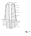
- Fig. 1 is a vertical sectional view of an antenna structure according to a first embodiment of the invention;
- Fig. 2A is an expanded plan view of an antenna element in the antenna structure of Fig. 1;
- Fig. 2B is a section view taken along a line IIB-IIB in Fig. 2A;
- Fig. 2C is a section view taken along a line IIC-IIC in Fig. 2A;
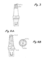
- Fig. 3 is a partial section view of a core member in the antenna structure of Fig. 1;
- Fig. 4A is a side view of the antenna structure of Fig. 1;
- Fig. 4B is a top view of the antenna structure of Fig. 1;
- Figs. 5A to 6 are views for explaining how to establish the electrical connection to the antenna element of Fig. 1;
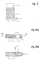
- Fig. 7 is an expanded plan view of an antenna element in an antenna structure according to a second embodiment of the invention;
- Fig. 8A is a side view of the antenna structure of Fig. 7;
- Fig. 8B is a section view taken along a line VIIIB-VIIIB in Fig. 8A;
- Fig. 9 is an enlarged section view showing how to establish the electrical connection to the antenna element of Fig. 7;
- Fig. 10 is an enlarged section view of a modified example of the antenna structure of Fig. 7;
- Fig. 11A is a section view of an antenna element in an antenna structure according to a third embodiment of the invention;
- Fig. 11 B is a plan view of the antenna element of Fig. 11A;
- Figs. 12 and 13 are section views showing how to establish the electrical connection to the antenna element of Fig. 11A;
- Fig. 14A is a side view of a first related-art antenna structure;
- Fig. 14B is an enlarged plan view of an antenna element in the antenna structure of Fig. 14A;
- Fig. 14C is a section view taken along a line XIVC-XIVC in Fig. 14A;
- Fig. 14D is a section view taken along a line XIVD-XIVD in Fig. 14A;
- Fig. 15A is an enlarged plan view of an antenna element in a second related-art antenna structure; and
- Fig. 15B is a section view of an electric contact part in the antenna structure of Fig. 15A.
-
- A first embodiment of the invention will be described below in detail with reference to Figs. 1 to 6.
- A
core member 20 formed of insulating resin or the like has an outer peripheral face substantially in a truncated conical shape, as shown in Fig. 3, to which anantenna element 22 is adapted to be adhered and fixed. Thecore member 20 is provided with ahole 20a passing through in an axial direction from a distal end face thereof. Theantenna element 22 is formed of a conductive foil made of a copper foil having a thickness of about 0.04mm. As shown in Fig. 2A, theantenna element 22 has an electrical contact part 22a at its one end, and a central part of the electrical contact part 22a is formed with two slits 22b intersecting at a right angle. An adhesive layer 22c is provided on a back face of theantenna element 22, and further, a pasteboard 22d is provided so as to cover the adhesive layer 22c. In addition, a cover tape 22e is provided on a surface of theantenna element 22 except at least the electrical contact part 22a, as shown in Figs. 2B and 2C. - It is to be noted that an adhesive layer 22c is omitted in Fig. 1, and the adhesive layer 22c and the cover tape 22e are omitted in Fig. 5.
- As a first step, the pasteboard 22d is removed, and the
antenna element 22 is adhered and fixed to thecore member 20, as shown in Fig. 4A and 4B. On this occasion, the electrical contact part 22a is adhered to the distal end face of thecore member 20 in such a manner that the electrical contact part 22a covers an opening end of thehole 20a of thecore member 20, and the slits 22b are opposed to thehole 20a. Further, as shown in Fig. 5A, a portion around the slits 22b of the electrical contact part 22a is folded into thehole 20a with ajig 24, and the folded portion is made to be adhered to an inner peripheral face of thehole 20a into a state shown in Fig. 5B. Thereafter, aconductive pin 26 is press-fitted into thehole 20a from the distal end face, as shown in Fig. 6. - Accordingly, as shown in Fig. 1, the portion of the electrical contact part 22a which has been folded into the
hole 20a is clamped between the inner peripheral face of thehole 20a and theconductive pin 26. The electrical contact part 22a is not provided with the cover tape 22e on the surface thereof, but directly press-fitted to theconductive pin 26, thereby to establish the electrical connection. An inserted tip end of theconductive pin 26 is appropriately calked with apower supply terminal 28 at a base end of thecore member 20 to establish the electrical connection. Thispower supply terminal 28 is electrically connected to an electric circuit inside a casing body, which is not shown. - In the antenna structure having the above described structure, the
conductive pin 26 is press-fitted to theantenna element 22 by clamping theantenna element 22, thereby to obtain the reliable electrical connection. Accordingly, the electrical connection of theantenna element 22 formed of the conductive foil can be established without necessity of the annoying work such as the soldering. - Next, a second embodiment of the invention will be described with reference to Figs. 7 to 9.
- An
antenna element 32 formed of a conductive foil is formed in a meander shape, and provided with an electrical contact part 32a at its one end. This electrical contact part 32a has three slits 32b which intersect at an equal angle to one another. A cover tape 32c is provided so as to avoid at least the electrical contact part 32a. Thisantenna element 32 is adhered and fixed to an outer peripheral face of acore member 30 in a columnar shape, and the electrical contact part 32a is adhered and fixed to the outer peripheral face of thecore member 30 in an intermediate part thereof. - The
core member 30 is provided with a hole 30a at a position where this electrical contact part 32a has been adhered and fixed, and the hole 30a is extended to reach apower supply terminal 38 which is integrally molded with thecore member 30. Thepower supply terminal 38 is provided with a hole 38a having a smaller diameter than the hole 30a and coaxial with the hole 30a. - In the same manner as in the first embodiment, after portions around the slits 32b are folded so as to be adhered and fixed to an inner peripheral face of the hole 30a, a
conductive pin 36 is inserted into the hole 30a. As shown in Fig. 9, thisconductive pin 36 clamps theantenna element 32 at the opening end of the hole 30a thereby to establish electrical connection, and a tip end of theconductive pin 36 is press-fitted into the hole 38a formed in thepower supply terminal 38 thereby to electrically connect theconductive pin 36 to thepower supply terminal 38. In this manner, theantenna element 32 and thepower supply terminal 38 can be electrically connected by way of theconductive pin 36. - Fig. 10 shows a modified example of the antenna structure of the second embodiment.
- In this example, a male thread 36a is engraved at the tip end portion of the
conductive pin 36, and a female thread 38b is engraved on an inner peripheral face of the hole 38a in thepower supply terminal 38. Theconductive pin 36 is press-fitted into the hole 30a of thecore member 30, and the male thread 36a of theconductive pin 36 is screwed with the female thread 38b of thepower supply terminal 38, so that the electrical contact part 32a of theantenna element 32 is clamped between the conductive 36 and the opening end of the hole 30a to establish the electrical connection. - Next, a third embodiment of the invention will be described with reference to Figs. 11 to 13.
- In this embodiment, an
antenna element 42 formed of a conductive foil is adhered and fixed to acarrier 40 formed of a dielectric body. Thecarrier 40 is provided with a hole 40a at a position where an electrical contact part 42a of theantenna element 42 is adhered and fixed. The electrical contact part 42a as shown in Fig. 11 is provided with an aperture 42b so as to be opposed to the hole 40a. Then, as shown in Fig. 12, the electrical contact part 42a is folded into the hole 40a by an outer peripheral face of a spring connector 44, and adhered to an inner peripheral face of the hole 40a. Thereafter, the spring connector 44 is press-fitted into the hole 40a, as shown in Fig. 13, and the folded portion of the electrical contact part 42a is clamped between the inner peripheral face of the hole 40a and the outer peripheral face of the spring connector 44, thereby to obtain the electrical connection. - In the first and second embodiments, the number of slits 22b, 32b may be arbitrary. Alternatively, an aperture may be formed in place of the slits, as in the third embodiment. Further, the electrical contact part need not be formed with the slits nor the aperture in advance, but an aperture may be appropriately opened in the conductive foil by pushing the
conductive pin jig 24 or the spring connector 44 through the conductive foil, so that the electrical contact part may be folded into thehole 20a, 30a, 40a. In this case, in a case where a tip end of thejig 24 is in a pyramidal shape, the slits corresponding to a crest of the pyramidal shape can be made in the conductive foil. - Although the outer peripheral face of the spring connector 44 is press-fitted into the hole 40a of the
carrier 40 in the third embodiment, the conductive pin may be press-fitted into the hole 40a. Alternatively, a tubular member formed of conductive material as a conductive pin may be press-fitted into the hole 40a of thecarrier 40, and then, the spring connector 44 may be press-fitted into this tubular member. Further, the spring connector in place of theconductive pin hole 20a, 30a in the first and second embodiments, while the conductive pin in place of the spring connector 44 may be press-fitted into the hole 40a in the third embodiment. It is also apparent that the electrical contact part 22a, 32a, 42a of theantenna element core member carrier 40.
Claims (13)
- An antenna, comprising:an insulative member, formed with a hole;an antenna element, provided as a conductive foil adhered onto the insulative member and having a contact section opposing to the hole; anda conductive member, fitted into the hole through the contact section of the antenna element, such that a part of the contact section is clamped between an outer face of the conductive member and an inner face of the hole.
- The antenna as set forth in claim 1, wherein the insulative member is a cylindrical core member of the antenna.
- The antenna as set forth in claim 1, wherein the insulative member is a dielectric carrier of the antenna.
- The antenna as set forth in claim 1, wherein the conductive member is a pin member.
- The antenna as set forth in claim 1, wherein the conductive member is a spring connector.
- The antenna as set forth in claim 1, wherein the part of the contact section of the antenna element is adhered onto the inner face of the hole.
- The antenna as set forth in claim 1, wherein a portion in the contact section of the antenna element through which the conductive member passes is formed with a slit in advance.
- The antenna as set forth in claim 1, wherein a portion in the contact section of the antenna element through which the conductive member passes is formed with an aperture in advance.
- The antenna as set forth in claim 2, wherein the hole extends in parallel to an axial direction of the cylindrical core member.
- The antenna as set forth in claim 2, wherein the hole extends perpendicularly to an axial direction of the cylindrical core member.
- A method of manufacturing an antenna, comprising steps of:providing an insulative member formed with a hole;adhering an antenna element having a contact section onto the insulative member such that the contact section opposes to the hole;folding a part of the contact section of the antenna element into the hole; andfitting a conductive member into the hole through the contact section of the antenna element, such that the part of the contact section is clamped between an outer face of the conductive member and an inner face of the hole.
- The manufacturing method as set forth in claim 11, wherein the part of the first section of the antenna element is folded by an external jig.
- The manufacturing method as set forth in claim 11, wherein the part of the first section of the antenna element is folded by the conductive member.
Applications Claiming Priority (2)
| Application Number | Priority Date | Filing Date | Title |
|---|---|---|---|
| JP2003338500A JP4181004B2 (en) | 2003-09-29 | 2003-09-29 | Antenna structure |
| JP2003338500 | 2003-09-29 |
Publications (1)
| Publication Number | Publication Date |
|---|---|
| EP1519441A1 true EP1519441A1 (en) | 2005-03-30 |
Family
ID=34191592
Family Applications (1)
| Application Number | Title | Priority Date | Filing Date |
|---|---|---|---|
| EP04022823A Withdrawn EP1519441A1 (en) | 2003-09-29 | 2004-09-24 | Antenna structure |
Country Status (5)
| Country | Link |
|---|---|
| US (1) | US7075488B2 (en) |
| EP (1) | EP1519441A1 (en) |
| JP (1) | JP4181004B2 (en) |
| KR (1) | KR100842779B1 (en) |
| CN (1) | CN1604391A (en) |
Cited By (1)
| Publication number | Priority date | Publication date | Assignee | Title |
|---|---|---|---|---|
| WO2007091954A1 (en) * | 2006-02-08 | 2007-08-16 | Laird Technologies Ab | An antenna arrangement for a portable radio coummunication device, and a portable radio communication device comprising such an antenna arrangement |
Families Citing this family (3)
| Publication number | Priority date | Publication date | Assignee | Title |
|---|---|---|---|---|
| JP4281116B2 (en) | 2007-04-27 | 2009-06-17 | 日本電気株式会社 | Power supply device |
| JP2011120129A (en) * | 2009-12-07 | 2011-06-16 | Panasonic Corp | Antenna and antenna device using the same |
| DE102015104297B4 (en) * | 2015-03-23 | 2018-10-11 | Lisa Dräxlmaier GmbH | Fixing element for connecting a circuit board, busbar and thus equipped power distributor of a vehicle |
Citations (4)
| Publication number | Priority date | Publication date | Assignee | Title |
|---|---|---|---|---|
| FR2736214A1 (en) * | 1995-06-29 | 1997-01-03 | Siemens Automotive Sa | METHOD FOR MOUNTING AN ELECTRICAL CONNECTION PIN ON A FLEXIBLE SUBSTRATE AND ELECTRONIC CIRCUIT FLAT AND MOUNTING RESULTING FROM THE IMPLEMENTATION OF THIS PROCESS |
| US6166697A (en) * | 1998-04-01 | 2000-12-26 | Allgon Ab | Antenna means, a method for its manufacturing and a hand-held radio communication device |
| WO2001024311A1 (en) * | 1999-09-27 | 2001-04-05 | Allgon Ab | An antenna device arranged to be connected to a piece of electric equipment |
| WO2002080304A1 (en) * | 2001-04-02 | 2002-10-10 | Allgon Mobile Communications Ab | An antenna arrangement |
Family Cites Families (4)
| Publication number | Priority date | Publication date | Assignee | Title |
|---|---|---|---|---|
| BR9708753A (en) * | 1996-04-16 | 1999-08-03 | Kyocera Corp | Portable radio communication device |
| JP3314654B2 (en) * | 1997-03-14 | 2002-08-12 | 日本電気株式会社 | Helical antenna |
| US5977931A (en) * | 1997-07-15 | 1999-11-02 | Antenex, Inc. | Low visibility radio antenna with dual polarization |
| JP4101514B2 (en) * | 1999-06-29 | 2008-06-18 | 三菱電機株式会社 | Antenna device |
-
2003
- 2003-09-29 JP JP2003338500A patent/JP4181004B2/en not_active Expired - Fee Related
-
2004
- 2004-09-24 KR KR1020040076975A patent/KR100842779B1/en not_active Expired - Fee Related
- 2004-09-24 EP EP04022823A patent/EP1519441A1/en not_active Withdrawn
- 2004-09-27 CN CNA200410012096XA patent/CN1604391A/en active Pending
- 2004-09-28 US US10/950,430 patent/US7075488B2/en not_active Expired - Fee Related
Patent Citations (4)
| Publication number | Priority date | Publication date | Assignee | Title |
|---|---|---|---|---|
| FR2736214A1 (en) * | 1995-06-29 | 1997-01-03 | Siemens Automotive Sa | METHOD FOR MOUNTING AN ELECTRICAL CONNECTION PIN ON A FLEXIBLE SUBSTRATE AND ELECTRONIC CIRCUIT FLAT AND MOUNTING RESULTING FROM THE IMPLEMENTATION OF THIS PROCESS |
| US6166697A (en) * | 1998-04-01 | 2000-12-26 | Allgon Ab | Antenna means, a method for its manufacturing and a hand-held radio communication device |
| WO2001024311A1 (en) * | 1999-09-27 | 2001-04-05 | Allgon Ab | An antenna device arranged to be connected to a piece of electric equipment |
| WO2002080304A1 (en) * | 2001-04-02 | 2002-10-10 | Allgon Mobile Communications Ab | An antenna arrangement |
Cited By (2)
| Publication number | Priority date | Publication date | Assignee | Title |
|---|---|---|---|---|
| WO2007091954A1 (en) * | 2006-02-08 | 2007-08-16 | Laird Technologies Ab | An antenna arrangement for a portable radio coummunication device, and a portable radio communication device comprising such an antenna arrangement |
| CN101379657B (en) * | 2006-02-08 | 2012-05-30 | 莱尔德技术股份有限公司 | Antenna device for portable radio communication device and portable radio communication device comprising such antenna device |
Also Published As
| Publication number | Publication date |
|---|---|
| JP4181004B2 (en) | 2008-11-12 |
| KR20050031420A (en) | 2005-04-06 |
| JP2005109738A (en) | 2005-04-21 |
| CN1604391A (en) | 2005-04-06 |
| KR100842779B1 (en) | 2008-07-02 |
| US7075488B2 (en) | 2006-07-11 |
| US20050068235A1 (en) | 2005-03-31 |
Similar Documents
| Publication | Publication Date | Title |
|---|---|---|
| US9692156B2 (en) | Electronic device | |
| US7736194B1 (en) | Universal electrical plug | |
| US5920252A (en) | High-voltage variable resistor | |
| US6128181A (en) | Electric component unit | |
| US4713633A (en) | Cover attaching arrangement for casing of dielectric coaxial resonators | |
| US5037329A (en) | Angular connector for a shielded coaxial cable | |
| JPH10214649A (en) | Spring connector and device using spring connector | |
| US6442036B2 (en) | Substrate mount type terminal | |
| JP3243201B2 (en) | Spring connector and device using the spring connector | |
| US8197284B2 (en) | Printed circuit board assembly and connecting method thereof | |
| JP2586334B2 (en) | Contact type high frequency signal connection structure | |
| US5281760A (en) | Terminal fitting for a high voltage resistor wire | |
| US7075488B2 (en) | Antenna structure | |
| US6800001B1 (en) | Socket connector for lead wire termination and method of using the same | |
| US20030186567A1 (en) | Electric connector for connecting electronic instruments | |
| JPH031501A (en) | Variable resistor | |
| US7081855B2 (en) | Multi piece puzzle-lock antenna using flex film radiator | |
| EP0692149B1 (en) | Electrical connector | |
| KR200497068Y1 (en) | Electrical connection terminal | |
| JPH0644131Y2 (en) | Substrate spacer | |
| CN111224265A (en) | Connector | |
| US20040043673A1 (en) | Connector and substrate for eletronic circuit fabrication | |
| CN216098526U (en) | Coaxial device mounting jig | |
| JP2666217B2 (en) | Manufacturing method of electrolytic capacitor | |
| JP3043715B2 (en) | Antenna for portable radio |
Legal Events
| Date | Code | Title | Description |
|---|---|---|---|
| PUAI | Public reference made under article 153(3) epc to a published international application that has entered the european phase |
Free format text: ORIGINAL CODE: 0009012 |
|
| AK | Designated contracting states |
Kind code of ref document: A1 Designated state(s): AT BE BG CH CY CZ DE DK EE ES FI FR GB GR HU IE IT LI LU MC NL PL PT RO SE SI SK TR |
|
| AX | Request for extension of the european patent |
Extension state: AL HR LT LV MK |
|
| AKX | Designation fees paid | ||
| REG | Reference to a national code |
Ref country code: DE Ref legal event code: 8566 |
|
| STAA | Information on the status of an ep patent application or granted ep patent |
Free format text: STATUS: THE APPLICATION IS DEEMED TO BE WITHDRAWN |
|
| 18D | Application deemed to be withdrawn |
Effective date: 20051001 |