EP1518824B1 - sp3 BOND BORON NITRIDE EMITTING LIGHT IN ULTRAVIOLET REGION, ITS PRODUCING METHOD, AND FUNCTIONAL MATERIAL USING SAME - Google Patents
sp3 BOND BORON NITRIDE EMITTING LIGHT IN ULTRAVIOLET REGION, ITS PRODUCING METHOD, AND FUNCTIONAL MATERIAL USING SAME Download PDFInfo
- Publication number
- EP1518824B1 EP1518824B1 EP03738617A EP03738617A EP1518824B1 EP 1518824 B1 EP1518824 B1 EP 1518824B1 EP 03738617 A EP03738617 A EP 03738617A EP 03738617 A EP03738617 A EP 03738617A EP 1518824 B1 EP1518824 B1 EP 1518824B1
- Authority
- EP
- European Patent Office
- Prior art keywords
- boron nitride
- reaction
- gas
- growing
- substrate
- Prior art date
- Legal status (The legal status is an assumption and is not a legal conclusion. Google has not performed a legal analysis and makes no representation as to the accuracy of the status listed.)
- Expired - Lifetime
Links
Images

Classifications
-
- C—CHEMISTRY; METALLURGY
- C09—DYES; PAINTS; POLISHES; NATURAL RESINS; ADHESIVES; COMPOSITIONS NOT OTHERWISE PROVIDED FOR; APPLICATIONS OF MATERIALS NOT OTHERWISE PROVIDED FOR
- C09K—MATERIALS FOR MISCELLANEOUS APPLICATIONS, NOT PROVIDED FOR ELSEWHERE
- C09K11/00—Luminescent materials, e.g. electroluminescent or chemiluminescent
- C09K11/08—Luminescent materials, e.g. electroluminescent or chemiluminescent containing inorganic luminescent materials
- C09K11/63—Luminescent materials, e.g. electroluminescent or chemiluminescent containing inorganic luminescent materials containing boron
-
- C—CHEMISTRY; METALLURGY
- C09—DYES; PAINTS; POLISHES; NATURAL RESINS; ADHESIVES; COMPOSITIONS NOT OTHERWISE PROVIDED FOR; APPLICATIONS OF MATERIALS NOT OTHERWISE PROVIDED FOR
- C09K—MATERIALS FOR MISCELLANEOUS APPLICATIONS, NOT PROVIDED FOR ELSEWHERE
- C09K11/00—Luminescent materials, e.g. electroluminescent or chemiluminescent
- C09K11/08—Luminescent materials, e.g. electroluminescent or chemiluminescent containing inorganic luminescent materials
- C09K11/0883—Arsenides; Nitrides; Phosphides
-
- C—CHEMISTRY; METALLURGY
- C23—COATING METALLIC MATERIAL; COATING MATERIAL WITH METALLIC MATERIAL; CHEMICAL SURFACE TREATMENT; DIFFUSION TREATMENT OF METALLIC MATERIAL; COATING BY VACUUM EVAPORATION, BY SPUTTERING, BY ION IMPLANTATION OR BY CHEMICAL VAPOUR DEPOSITION, IN GENERAL; INHIBITING CORROSION OF METALLIC MATERIAL OR INCRUSTATION IN GENERAL
- C23C—COATING METALLIC MATERIAL; COATING MATERIAL WITH METALLIC MATERIAL; SURFACE TREATMENT OF METALLIC MATERIAL BY DIFFUSION INTO THE SURFACE, BY CHEMICAL CONVERSION OR SUBSTITUTION; COATING BY VACUUM EVAPORATION, BY SPUTTERING, BY ION IMPLANTATION OR BY CHEMICAL VAPOUR DEPOSITION, IN GENERAL
- C23C14/00—Coating by vacuum evaporation, by sputtering or by ion implantation of the coating forming material
- C23C14/0021—Reactive sputtering or evaporation
- C23C14/0026—Activation or excitation of reactive gases outside the coating chamber
-
- C—CHEMISTRY; METALLURGY
- C23—COATING METALLIC MATERIAL; COATING MATERIAL WITH METALLIC MATERIAL; CHEMICAL SURFACE TREATMENT; DIFFUSION TREATMENT OF METALLIC MATERIAL; COATING BY VACUUM EVAPORATION, BY SPUTTERING, BY ION IMPLANTATION OR BY CHEMICAL VAPOUR DEPOSITION, IN GENERAL; INHIBITING CORROSION OF METALLIC MATERIAL OR INCRUSTATION IN GENERAL
- C23C—COATING METALLIC MATERIAL; COATING MATERIAL WITH METALLIC MATERIAL; SURFACE TREATMENT OF METALLIC MATERIAL BY DIFFUSION INTO THE SURFACE, BY CHEMICAL CONVERSION OR SUBSTITUTION; COATING BY VACUUM EVAPORATION, BY SPUTTERING, BY ION IMPLANTATION OR BY CHEMICAL VAPOUR DEPOSITION, IN GENERAL
- C23C14/00—Coating by vacuum evaporation, by sputtering or by ion implantation of the coating forming material
- C23C14/06—Coating by vacuum evaporation, by sputtering or by ion implantation of the coating forming material characterised by the coating material
- C23C14/0641—Nitrides
- C23C14/0647—Boron nitride
-
- C—CHEMISTRY; METALLURGY
- C23—COATING METALLIC MATERIAL; COATING MATERIAL WITH METALLIC MATERIAL; CHEMICAL SURFACE TREATMENT; DIFFUSION TREATMENT OF METALLIC MATERIAL; COATING BY VACUUM EVAPORATION, BY SPUTTERING, BY ION IMPLANTATION OR BY CHEMICAL VAPOUR DEPOSITION, IN GENERAL; INHIBITING CORROSION OF METALLIC MATERIAL OR INCRUSTATION IN GENERAL
- C23C—COATING METALLIC MATERIAL; COATING MATERIAL WITH METALLIC MATERIAL; SURFACE TREATMENT OF METALLIC MATERIAL BY DIFFUSION INTO THE SURFACE, BY CHEMICAL CONVERSION OR SUBSTITUTION; COATING BY VACUUM EVAPORATION, BY SPUTTERING, BY ION IMPLANTATION OR BY CHEMICAL VAPOUR DEPOSITION, IN GENERAL
- C23C14/00—Coating by vacuum evaporation, by sputtering or by ion implantation of the coating forming material
- C23C14/22—Coating by vacuum evaporation, by sputtering or by ion implantation of the coating forming material characterised by the process of coating
- C23C14/24—Vacuum evaporation
- C23C14/28—Vacuum evaporation by wave energy or particle radiation
-
- C—CHEMISTRY; METALLURGY
- C23—COATING METALLIC MATERIAL; COATING MATERIAL WITH METALLIC MATERIAL; CHEMICAL SURFACE TREATMENT; DIFFUSION TREATMENT OF METALLIC MATERIAL; COATING BY VACUUM EVAPORATION, BY SPUTTERING, BY ION IMPLANTATION OR BY CHEMICAL VAPOUR DEPOSITION, IN GENERAL; INHIBITING CORROSION OF METALLIC MATERIAL OR INCRUSTATION IN GENERAL
- C23C—COATING METALLIC MATERIAL; COATING MATERIAL WITH METALLIC MATERIAL; SURFACE TREATMENT OF METALLIC MATERIAL BY DIFFUSION INTO THE SURFACE, BY CHEMICAL CONVERSION OR SUBSTITUTION; COATING BY VACUUM EVAPORATION, BY SPUTTERING, BY ION IMPLANTATION OR BY CHEMICAL VAPOUR DEPOSITION, IN GENERAL
- C23C16/00—Chemical coating by decomposition of gaseous compounds, without leaving reaction products of surface material in the coating, i.e. chemical vapour deposition [CVD] processes
- C23C16/22—Chemical coating by decomposition of gaseous compounds, without leaving reaction products of surface material in the coating, i.e. chemical vapour deposition [CVD] processes characterised by the deposition of inorganic material, other than metallic material
- C23C16/30—Deposition of compounds, mixtures or solid solutions, e.g. borides, carbides, nitrides
- C23C16/34—Nitrides
- C23C16/342—Boron nitride
-
- C—CHEMISTRY; METALLURGY
- C23—COATING METALLIC MATERIAL; COATING MATERIAL WITH METALLIC MATERIAL; CHEMICAL SURFACE TREATMENT; DIFFUSION TREATMENT OF METALLIC MATERIAL; COATING BY VACUUM EVAPORATION, BY SPUTTERING, BY ION IMPLANTATION OR BY CHEMICAL VAPOUR DEPOSITION, IN GENERAL; INHIBITING CORROSION OF METALLIC MATERIAL OR INCRUSTATION IN GENERAL
- C23C—COATING METALLIC MATERIAL; COATING MATERIAL WITH METALLIC MATERIAL; SURFACE TREATMENT OF METALLIC MATERIAL BY DIFFUSION INTO THE SURFACE, BY CHEMICAL CONVERSION OR SUBSTITUTION; COATING BY VACUUM EVAPORATION, BY SPUTTERING, BY ION IMPLANTATION OR BY CHEMICAL VAPOUR DEPOSITION, IN GENERAL
- C23C16/00—Chemical coating by decomposition of gaseous compounds, without leaving reaction products of surface material in the coating, i.e. chemical vapour deposition [CVD] processes
- C23C16/44—Chemical coating by decomposition of gaseous compounds, without leaving reaction products of surface material in the coating, i.e. chemical vapour deposition [CVD] processes characterised by the method of coating
- C23C16/48—Chemical coating by decomposition of gaseous compounds, without leaving reaction products of surface material in the coating, i.e. chemical vapour deposition [CVD] processes characterised by the method of coating by irradiation, e.g. photolysis, radiolysis, particle radiation
- C23C16/482—Chemical coating by decomposition of gaseous compounds, without leaving reaction products of surface material in the coating, i.e. chemical vapour deposition [CVD] processes characterised by the method of coating by irradiation, e.g. photolysis, radiolysis, particle radiation using incoherent light, UV to IR, e.g. lamps
-
- C—CHEMISTRY; METALLURGY
- C23—COATING METALLIC MATERIAL; COATING MATERIAL WITH METALLIC MATERIAL; CHEMICAL SURFACE TREATMENT; DIFFUSION TREATMENT OF METALLIC MATERIAL; COATING BY VACUUM EVAPORATION, BY SPUTTERING, BY ION IMPLANTATION OR BY CHEMICAL VAPOUR DEPOSITION, IN GENERAL; INHIBITING CORROSION OF METALLIC MATERIAL OR INCRUSTATION IN GENERAL
- C23C—COATING METALLIC MATERIAL; COATING MATERIAL WITH METALLIC MATERIAL; SURFACE TREATMENT OF METALLIC MATERIAL BY DIFFUSION INTO THE SURFACE, BY CHEMICAL CONVERSION OR SUBSTITUTION; COATING BY VACUUM EVAPORATION, BY SPUTTERING, BY ION IMPLANTATION OR BY CHEMICAL VAPOUR DEPOSITION, IN GENERAL
- C23C16/00—Chemical coating by decomposition of gaseous compounds, without leaving reaction products of surface material in the coating, i.e. chemical vapour deposition [CVD] processes
- C23C16/44—Chemical coating by decomposition of gaseous compounds, without leaving reaction products of surface material in the coating, i.e. chemical vapour deposition [CVD] processes characterised by the method of coating
- C23C16/50—Chemical coating by decomposition of gaseous compounds, without leaving reaction products of surface material in the coating, i.e. chemical vapour deposition [CVD] processes characterised by the method of coating using electric discharges
-
- C—CHEMISTRY; METALLURGY
- C23—COATING METALLIC MATERIAL; COATING MATERIAL WITH METALLIC MATERIAL; CHEMICAL SURFACE TREATMENT; DIFFUSION TREATMENT OF METALLIC MATERIAL; COATING BY VACUUM EVAPORATION, BY SPUTTERING, BY ION IMPLANTATION OR BY CHEMICAL VAPOUR DEPOSITION, IN GENERAL; INHIBITING CORROSION OF METALLIC MATERIAL OR INCRUSTATION IN GENERAL
- C23C—COATING METALLIC MATERIAL; COATING MATERIAL WITH METALLIC MATERIAL; SURFACE TREATMENT OF METALLIC MATERIAL BY DIFFUSION INTO THE SURFACE, BY CHEMICAL CONVERSION OR SUBSTITUTION; COATING BY VACUUM EVAPORATION, BY SPUTTERING, BY ION IMPLANTATION OR BY CHEMICAL VAPOUR DEPOSITION, IN GENERAL
- C23C16/00—Chemical coating by decomposition of gaseous compounds, without leaving reaction products of surface material in the coating, i.e. chemical vapour deposition [CVD] processes
- C23C16/44—Chemical coating by decomposition of gaseous compounds, without leaving reaction products of surface material in the coating, i.e. chemical vapour deposition [CVD] processes characterised by the method of coating
- C23C16/50—Chemical coating by decomposition of gaseous compounds, without leaving reaction products of surface material in the coating, i.e. chemical vapour deposition [CVD] processes characterised by the method of coating using electric discharges
- C23C16/513—Chemical coating by decomposition of gaseous compounds, without leaving reaction products of surface material in the coating, i.e. chemical vapour deposition [CVD] processes characterised by the method of coating using electric discharges using plasma jets
Definitions
- the present invention relates to a sp3-bonded boron nitride, represented by a general formula "BN", and, more particularly, to a sp3-bonded boron nitride having a new crystalline structure having a hexagonal 5H or 6H polytypic form, a producing method of the same, and applications utilizing the properties of the same.
- BN sp3-bonded boron nitride
- the present invention relates to a sp3-bonded boron nitride, represented by a general formula "BN", which has a hexagonal 5H or 6H polytypic form and a property of emitting light in ultraviolet region and which can be used as electronic materials, particularly light-emitting diode, ultraviolet solid-state laser, electron-emitting material, and surface coating material on cutting tool.
- BN sp3-bonded boron nitride
- Boron nitride is a material having been mainly used for industrial applications as heat resistant and abrasion-resistant materials. Recently, boron nitride has been also put as a subject of research as a part of research and development of boron compounds expected to develop new products and has received considerable attention.
- sp3-bonded BNs are of cubic phase (3C polytypic form) and wurtzite form (2H polytypic form).
- the technical feature of the first aspect is to disclose the composition of the boron nitride having a novel structure and property which is the aim of the present invention.
- the first aspect is (1) a sp3-bonded boron nitride, represented by a general formula BN, having a hexagonal 5H or 6H polytypic form and having a property of emitting light in ultraviolet region.
- the technical features described in the second through eighth aspect are to disclose production methods of the boron nitride composition of the first invention.
- the second aspect is (2) a producing method of a sp3-bonded boron nitride, represented by a general formula BN, having a hexagonal 5H or 6H polytypic form and having a property of emitting light in ultraviolet region, the method comprising: introducing reaction mixed gas containing boron and nitrogen being diluted with dilution gas into a reaction chamber; and irradiating a surface of a substrate placed in the chamber, a growing surface on the substrate, and a growing spacing region about the growing surface with ultraviolet light to cause gas phase reaction, thereby generating, depositing, or growing a sp3-bonded boron nitride, represented by a general formula BN, having a hexagonal 5H or 6H polytypic form and having a property of emitting light in ultraviolet region on the substrate.
- a sp3-bonded boron nitride represented by a general formula BN, having a hexagonal 5H or 6H polytypic form and having a property of emit
- the third aspect is (3) a producing method of a sp3-bonded boron nitride, represented by a general formula BN, having a hexagonal 5H or 6H polytypic form and having a property of emitting light in ultraviolet region, as stated in the above (2), wherein the dilution gas is noble gas, hydrogen, nitrogen, or mixed gas consisting of two or more of these and the ratio of the reaction gas to the dilution gas is 100:0.0001-100 by volume,
- the fourth invention is (4) a producing method of a sp3-bonded boron nitride, represented by a general formula BN, having a hexagonal 5H or 6H polytypic form and having a property of emitting light in ultraviolet region, the method comprising, inserting boron nitride as a boron raw material into a reaction chamber while introducing reaction mixed gas containing nitrogen being diluted with dilution gas into the reaction chamber; converging and emitting ultraviolet laser of from 190 nm to 400 nm wavelength onto the boron nitride solid raw material so as to vaporize, generate radical containing boron or BN precursor matter; and irradiating a surface of a substrate placed in the chamber, a growing surface on the substrate, and a growing spacing region about the growing surface with ultraviolet light to cause gas phase reaction between the reaction gas containing nitrogen and the radical containing boron or re-coagulation reaction of the BN precursor matter in the vaporized state, thereby generating, deposit
- the fifth aspect is (5) a producing method of a sp3-bonded boron nitride, represented by a general formula BN, having a hexagonal 5H or 6H polytypic form and having a property of emitting light in ultraviolet region, the method comprising: inserting boron nitride as a boron raw material into a reaction chamber while introducing reaction mixed gas containing boron and nitrogen being diluted with dilution gas into the reaction chamber; irradiating the boron nitride solid raw material with plasma as well as ultraviolet laser of from 190 nm to 400 nm wavelength so as to vaporize, generate radical containing boron or BN precursor matter; and irradiating a surface of a substrate placed in the chamber, a growing surface on the substrate, and a growing spacing region about the growing surface with ultraviolet light to cause gas phase reaction between the reaction gas containing nitrogen and the radical containing boron or re-coagulation reaction of the BN precursor matter in the vaporized state
- the sixth aspect is (6) a producing method of a sp3-bonded boron nitride, represented by a general formula BN, having a hexagonal 5H or 6H polytypic form and having a property of emitting light in ultraviolet region, as stated in the above (4) or (5), wherein the dilution gas is noble gas, hydrogen, nitrogen, or mixed gas consisting of two or more of these and the ratio of the reaction gas to the dilution gas is 100:0-100% by volume.
- the dilution gas is noble gas, hydrogen, nitrogen, or mixed gas consisting of two or more of these and the ratio of the reaction gas to the dilution gas is 100:0-100% by volume.
- the seventh aspect is (7) a producing method of a sp3-bonded boron nitride, represented by a general formula BN, having a hexagonal 5H or 6H polytypic form and having a property of emitting light in ultraviolet region, as stated in the above (4) or (5), wherein the ultraviolet laser is pulse laser.
- the eighth aspect is (8) a producing method of a sp3-bonded boron nitride, represented by a general formula BN, having a hexagonal 5H or 6H polytypic form and having a property of emitting light in ultraviolet region, as stated in the above (5) or (7), wherein by applying modulation synchronizing laser pulse onto the plasma, the plasma is packeted so as to generate, deposit, and grow a sp3-bonded boron nitride, represented by a general formula BN, having a hexagonal 5H or 6H polytypic form and having a property of emitting light in ultraviolet region and which has improved crystalline property.
- the ninth aspect is (9) a functional material containing a sp3-bonded boron nitride, represented by a general formula BN, having a hexagonal 5H or 6H polytypic form and having a property of emitting light in ultraviolet region as stated in the above (1), wherein the functional material is used for applications utilizing the properties of the boron nitride compound contained therein.
- a functional material containing a sp3-bonded boron nitride represented by a general formula BN, having a hexagonal 5H or 6H polytypic form and having a property of emitting light in ultraviolet region as stated in the above (1), wherein the functional material is used for applications utilizing the properties of the boron nitride compound contained therein.
- the tenth aspect is (10) a functional material as stated in the above (9), wherein the functional material is used mainly as material emitting light in ultraviolet region.
- the eleventh aspect is (11) a functional material stated in the above (9), wherein the functional material is used mainly as an electronic material, particularly light-emitting diode.
- the twelfth aspect is (12) a functional material as stated in the above (9), wherein the functional material is used mainly as surface coating material on cutting tool.
- the content described in the above (1) discloses a structure of a compound which is the aim of the present invention, that is, a sp3-bonded boron nitride, represented by a general formula BN, having a hexagonal 5H or 6H polytypic form and having a property of emitting light in ultraviolet region.
- sp3-bonded BNs are of cubic phase (3C polytypic form) and wurtzite form (2H polytypic form), while the compound of the present invention according to the aforementioned structure has a hexagonal 5H or 6H polytypic form completely different from the conventionally known BNs and has a property of emitting light in ultraviolet region, as mentioned above.
- the present invention provides a boron nitride having radically nobel structure and characteristics.
- the reaction chamber used herein is a CVD reaction chamber of which schematic structure is shown in Fig. 1 .
- the reaction chamber 1 comprises a gas introduction port 2 for introduction of reaction gas and dilution gas therefore and a gas exhaust 3 for exhausting the introduced reaction gas and the like to the outside of the chamber and is connected to a vacuum pump so that the inner pressure is maintained at a reduced pressure below the atmospheric pressure.
- a boron nitride deposition substrate 4 is placed on the way of gas flow.
- An optical window 5 is mounted in a part of a wall of the reaction chamber facing the substrate.
- An excimer ultraviolet laser equipment 6 is set in such a manner that the substrate is irradiated with ultraviolet light through the window.
- the reaction gas introduced into the reaction chamber is excited by the ultraviolet light incident on the substrate surface so as to cause gas phase reaction between nitrogen source and boron source in the reaction gas, thereby generating, depositing, or growing a sp3-bonded boron nitride, represented by a general formula BN, having a hexagonal 5H or 6H polytypic form and having a property of emitting light in ultraviolet region.
- a sp3-bonded boron nitride represented by a general formula BN, having a hexagonal 5H or 6H polytypic form and having a property of emitting light in ultraviolet region.
- a plasma torch 7 is provided for this embodiment.
- the reaction gas introduction port and the plasma torch are formed as united part facing the substrate so that the reaction gas and the plasma are directed to the substrate.
- a boron nitride solid material as the boron source.
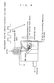
- Fig. 4 shows the aspect of the reaction in this case. That is, a BN target and a substrate are previously placed in the reaction chamber.
- the disclosed examples show embodiments in which only ammonia gas diluted with Ar gas is introduced as nitrogen source gas as the reaction gas into the reaction chamber through the plasma torch nozzle, embodiments are not limited thereto. That is, it is apparent to a person with ordinary skill in the art that, besides ammonia, gas containing nitrogen or other noble gas can be also used.
- the introduced gas is plasmarized and is directed to the BN target.
- the target is irradiated with exima laser as well as the plasma whereby the target is vaporized its components so as to generate radials of nitrogen and boron or a BN series precursor matter.
- a desired compound i.e. a sp3-bonded boron nitride, represented by a general formula "BN", having a hexagonal 5H or 6H polytypic form and having a property of emitting light in ultraviolet region, is deposited or grown on the substrate.
- the present invention aims to provide a sp3-bonded boron nitride, represented by a general formula "BN", having a hexagonal 5H or 6H polytypic form and a property of emitting light in ultraviolet region, a production method of the same, and applications utilizing the properties of the same, as mentioned above.
- BN sp3-bonded boron nitride
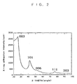
- the X-ray diffraction pattern is shown in Fig. 2 .
- the diffraction results of this pattern are shown in Table 1.
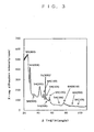
- the X-ray diffraction pattern is shown in Fig. 3 .
- the diffraction results of this pattern are shown in Table 2.
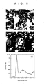
- Fig. 6(b) is an image of cathode luminescence caused by irradiation of electron beam of 20KeV, the cathode luminescence image at 230 nm being taken. It is found that UV emission appears over the entire area of the sample.
- Fig. 6(c) shows a spectrum obtained from the cathode luminescence caused by irradiation of electron beam of 20KeV. It is found that there is sharp luminescence at 225 nm. It is found that there is broad UV emission is present at 300 nm.
- a sp3-bonded hexagonal BN of 5H or 6H type has sharp emission at ultraviolet wavelength of 225 nm which is in a range capable of being used in atmosphere but almost borders on a region of vacuum ultraviolet, the BN has great potential as materials for practical application of solid ultraviolet laser.
- the practical application of solid ultraviolet laser will make immeasurable technical spillover effects on dramatic increase in capacity of rewritable recording media, chemistry, medicine, electronics industry, and others.
Landscapes
- Chemical & Material Sciences (AREA)
- Engineering & Computer Science (AREA)
- Materials Engineering (AREA)
- Organic Chemistry (AREA)
- Chemical Kinetics & Catalysis (AREA)
- Mechanical Engineering (AREA)
- Metallurgy (AREA)
- General Chemical & Material Sciences (AREA)
- Plasma & Fusion (AREA)
- Physics & Mathematics (AREA)
- Inorganic Chemistry (AREA)
- Toxicology (AREA)
- Health & Medical Sciences (AREA)
- Chemical Vapour Deposition (AREA)
- Crystals, And After-Treatments Of Crystals (AREA)
- Physical Vapour Deposition (AREA)
- Led Devices (AREA)
- Luminescent Compositions (AREA)
Description
- The present invention relates to a sp3-bonded boron nitride, represented by a general formula "BN", and, more particularly, to a sp3-bonded boron nitride having a new crystalline structure having a hexagonal 5H or 6H polytypic form, a producing method of the same, and applications utilizing the properties of the same. That is, the present invention relates to a sp3-bonded boron nitride, represented by a general formula "BN", which has a hexagonal 5H or 6H polytypic form and a property of emitting light in ultraviolet region and which can be used as electronic materials, particularly light-emitting diode, ultraviolet solid-state laser, electron-emitting material, and surface coating material on cutting tool.
- Boron nitride is a material having been mainly used for industrial applications as heat resistant and abrasion-resistant materials. Recently, boron nitride has been also put as a subject of research as a part of research and development of boron compounds expected to develop new products and has received considerable attention.
- Currently known sp3-bonded BNs are of cubic phase (3C polytypic form) and wurtzite form (2H polytypic form).
- As a result that inventors of this invention have earnestly studied sp3-bonded boron nitride, represented by a general formula "BN", as a part of the aforementioned research, the inventors found a sp3-bonded boron nitride which has quite new crystalline structure and a very interesting, important, and specific property of emitting light in ultraviolet region. This invention was made on the basis of this finding. That is, the present invention provides a boron nitride having new crystalline structure, a producing method of the same, and applications of the same.
- As a result of further earnest studies about sp3-bonded boron nitride, the inventors succeeded in providing a boron nitride having a novel structure and property, producing it with repeatability, and providing material to be used for new applications utilizing its specific properties according to technical features as defined in the claims.
- The implemented technical features are based on the requirements described in the following aspects (1)-(12).
- The technical feature of the first aspect is to disclose the composition of the boron nitride having a novel structure and property which is the aim of the present invention.
- That is, the first aspect is (1) a sp3-bonded boron nitride, represented by a general formula BN, having a hexagonal 5H or 6H polytypic form and having a property of emitting light in ultraviolet region.
- The technical features described in the second through eighth aspect are to disclose production methods of the boron nitride composition of the first invention.
- That is, the second aspect is (2) a producing method of a sp3-bonded boron nitride, represented by a general formula BN, having a hexagonal 5H or 6H polytypic form and having a property of emitting light in ultraviolet region, the method comprising: introducing reaction mixed gas containing boron and nitrogen being diluted with dilution gas into a reaction chamber; and irradiating a surface of a substrate placed in the chamber, a growing surface on the substrate, and a growing spacing region about the growing surface with ultraviolet light to cause gas phase reaction, thereby generating, depositing, or growing a sp3-bonded boron nitride, represented by a general formula BN, having a hexagonal 5H or 6H polytypic form and having a property of emitting light in ultraviolet region on the substrate.
- The third aspect is (3) a producing method of a sp3-bonded boron nitride, represented by a general formula BN, having a hexagonal 5H or 6H polytypic form and having a property of emitting light in ultraviolet region, as stated in the above (2), wherein the dilution gas is noble gas, hydrogen, nitrogen, or mixed gas consisting of two or more of these and the ratio of the reaction gas to the dilution gas is 100:0.0001-100 by volume,
- The fourth invention is (4) a producing method of a sp3-bonded boron nitride, represented by a general formula BN, having a hexagonal 5H or 6H polytypic form and having a property of emitting light in ultraviolet region, the method comprising, inserting boron nitride as a boron raw material into a reaction chamber while introducing reaction mixed gas containing nitrogen being diluted with dilution gas into the reaction chamber; converging and emitting ultraviolet laser of from 190 nm to 400 nm wavelength onto the boron nitride solid raw material so as to vaporize, generate radical containing boron or BN precursor matter; and irradiating a surface of a substrate placed in the chamber, a growing surface on the substrate, and a growing spacing region about the growing surface with ultraviolet light to cause gas phase reaction between the reaction gas containing nitrogen and the radical containing boron or re-coagulation reaction of the BN precursor matter in the vaporized state, thereby generating, depositing, or growing a sp3-bonded boron nitride, represented by a general formula BN, having a hexagonal 5H or 6H polytypic form and having a property of emitting light in ultraviolet region on the substrate.
- The fifth aspect is (5) a producing method of a sp3-bonded boron nitride, represented by a general formula BN, having a hexagonal 5H or 6H polytypic form and having a property of emitting light in ultraviolet region, the method comprising: inserting boron nitride as a boron raw material into a reaction chamber while introducing reaction mixed gas containing boron and nitrogen being diluted with dilution gas into the reaction chamber; irradiating the boron nitride solid raw material with plasma as well as ultraviolet laser of from 190 nm to 400 nm wavelength so as to vaporize, generate radical containing boron or BN precursor matter; and irradiating a surface of a substrate placed in the chamber, a growing surface on the substrate, and a growing spacing region about the growing surface with ultraviolet light to cause gas phase reaction between the reaction gas containing nitrogen and the radical containing boron or re-coagulation reaction of the BN precursor matter in the vaporized state, thereby generating, depositing, or growing a sp3-bonded boron nitride, represented by a general formula BN, having a hexagonal 5H or 6H polytypic form and having a property of emitting light in ultraviolet region on the substrate.
- The sixth aspect is (6) a producing method of a sp3-bonded boron nitride, represented by a general formula BN, having a hexagonal 5H or 6H polytypic form and having a property of emitting light in ultraviolet region, as stated in the above (4) or (5), wherein the dilution gas is noble gas, hydrogen, nitrogen, or mixed gas consisting of two or more of these and the ratio of the reaction gas to the dilution gas is 100:0-100% by volume.
- The seventh aspect is (7) a producing method of a sp3-bonded boron nitride, represented by a general formula BN, having a hexagonal 5H or 6H polytypic form and having a property of emitting light in ultraviolet region, as stated in the above (4) or (5), wherein the ultraviolet laser is pulse laser.
- The eighth aspect is (8) a producing method of a sp3-bonded boron nitride, represented by a general formula BN, having a hexagonal 5H or 6H polytypic form and having a property of emitting light in ultraviolet region, as stated in the above (5) or (7), wherein by applying modulation synchronizing laser pulse onto the plasma, the plasma is packeted so as to generate, deposit, and grow a sp3-bonded boron nitride, represented by a general formula BN, having a hexagonal 5H or 6H polytypic form and having a property of emitting light in ultraviolet region and which has improved crystalline property.
- The technical features in the ninth through twelfth aspect are described to disclose applications of the boron nitride composition of the first aspect.
- That is, the ninth aspect is (9) a functional material containing a sp3-bonded boron nitride, represented by a general formula BN, having a hexagonal 5H or 6H polytypic form and having a property of emitting light in ultraviolet region as stated in the above (1), wherein the functional material is used for applications utilizing the properties of the boron nitride compound contained therein.
- The tenth aspect is (10) a functional material as stated in the above (9), wherein the functional material is used mainly as material emitting light in ultraviolet region.
- The eleventh aspect is (11) a functional material stated in the above (9), wherein the functional material is used mainly as an electronic material, particularly light-emitting diode.
- The twelfth aspect is (12) a functional material as stated in the above (9), wherein the functional material is used mainly as surface coating material on cutting tool.
- The content described in the above (1) discloses a structure of a compound which is the aim of the present invention, that is, a sp3-bonded boron nitride, represented by a general formula BN, having a hexagonal 5H or 6H polytypic form and having a property of emitting light in ultraviolet region.
- Currently known sp3-bonded BNs are of cubic phase (3C polytypic form) and wurtzite form (2H polytypic form), while the compound of the present invention according to the aforementioned structure has a hexagonal 5H or 6H polytypic form completely different from the conventionally known BNs and has a property of emitting light in ultraviolet region, as mentioned above.
- Until now, no boron nitride emitting light in ultraviolet region (200-400 nm) has been known and no BN having a hexagonal 5H or 6H polytypic form and emitting light in ultraviolet region has been obtained. That is, the present invention provides a boron nitride having radically nobel structure and characteristics.
- The features in the above (2) through (8) are described to disclose producing methods for the nobel boron nitride structured as described in (1), thereby producing the boron nitride with repeatability.
- The reaction chamber used herein is a CVD reaction chamber of which schematic structure is shown in
Fig. 1 . InFig. 1 , thereaction chamber 1 comprises agas introduction port 2 for introduction of reaction gas and dilution gas therefore and agas exhaust 3 for exhausting the introduced reaction gas and the like to the outside of the chamber and is connected to a vacuum pump so that the inner pressure is maintained at a reduced pressure below the atmospheric pressure. In the chamber, a boronnitride deposition substrate 4 is placed on the way of gas flow. Anoptical window 5 is mounted in a part of a wall of the reaction chamber facing the substrate. An excimerultraviolet laser equipment 6 is set in such a manner that the substrate is irradiated with ultraviolet light through the window. - The reaction gas introduced into the reaction chamber is excited by the ultraviolet light incident on the substrate surface so as to cause gas phase reaction between nitrogen source and boron source in the reaction gas, thereby generating, depositing, or growing a sp3-bonded boron nitride, represented by a general formula BN, having a hexagonal 5H or 6H polytypic form and having a property of emitting light in ultraviolet region. It was apparent from experiments that the practical range of inner pressure of the reaction chamber is wide, i.e. from 0.133 Pa to 101 kPa (0.001 to 760 Torr), and the practical range of temperature of the substrate is also wide, i.e. from room temperature to 1200°C: However, to obtain high-purity reaction product as desired compound, the reaction is preferably conducted with lower pressure and higher temperature.
- Irradiating the substrate surface and a spacing range near the substrate with plasma as well as ultraviolet light for exciting the reaction gas is also practicable as another embodiment. In
Fig. 1 , aplasma torch 7 is provided for this embodiment. In this configuration, the reaction gas introduction port and the plasma torch are formed as united part facing the substrate so that the reaction gas and the plasma are directed to the substrate. - Though mixed gas containing nitrogen source and boron source can be used as the reaction material in the constitutions of the aforementioned inventions (2) through (8), the inventions described in (4) through (8) disclose the constitutions in case of using a boron nitride solid material as the boron source.
Fig. 4 shows the aspect of the reaction in this case. That is, a BN target and a substrate are previously placed in the reaction chamber. Though the disclosed examples show embodiments in which only ammonia gas diluted with Ar gas is introduced as nitrogen source gas as the reaction gas into the reaction chamber through the plasma torch nozzle, embodiments are not limited thereto. That is, it is apparent to a person with ordinary skill in the art that, besides ammonia, gas containing nitrogen or other noble gas can be also used. - Anyway, the introduced gas is plasmarized and is directed to the BN target. The target is irradiated with exima laser as well as the plasma whereby the target is vaporized its components so as to generate radials of nitrogen and boron or a BN series precursor matter. By the gas phase reaction of the generated radicals or the re-coagulation reaction of vaporized component, a desired compound, i.e. a sp3-bonded boron nitride, represented by a general formula "BN", having a hexagonal 5H or 6H polytypic form and having a property of emitting light in ultraviolet region, is deposited or grown on the substrate.
- It was apparent similarly to the above invention (2) that the practical range of inner pressure of the reaction chamber is wide, i.e. from 0.133 Pa to 101 kPa (0.001 to 760 Torr), and the practical range of temperature of the substrate is also wide, i.e. from room temperature to 1200°C. Reaction products are also attached to the optical window for irradiation of excimer laser fixed in the redaction chamber, reducing the transmission of laser beam and thus inhibiting the reaction for obtaining the desired compound. Therefore, it is important to take measures for preventing such deposition on the optical window and/or portions of wall of the chamber where deposition is disadvantageous. As a specific means, argon gas is sprayed onto the optical window so as to form a kind of air curtain.
- In the embodiment using the boron nitride target, it was apparent from experiments that means of applying modulation synchronizing excimer laser onto the plasma to packet the plasma is effective in increasing the crystalline property of the desired compound. Invention (8) discloses this embodiment.
-
Fig. 1 is an illustration showing the outline of a synthesis reaction chamber of the present invention and a synthesis state; -
Fig. 2 is an X-ray diffraction pattern of a sp3-bonded BN of hexagonal 5H polytypic form (Example 1) of the present invention; -
Fig. 3 is an X-ray diffraction pattern of a sp3-bonded BN of hexagonal 6H polytypic form (Example 2) of the present invention; -
Fig. 4 is an illustration showing the outline of a synthesis reaction chamber of the present invention and a synthesis state using this chamber; -
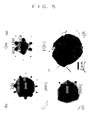
Fig. 5 is an electron diffraction pattern of a sp3-bonded BN of hexagonal 5H polytypic form (Example 5) of the present invention; and -
Figs. 6(a)-6(c) are an SEM image (Fig. 6(a) ), a CL image (Fig. 6(b) ), and a CL spectrum of a sp3-bonded BN of hexagonal 5H polytypic form (Example 7) of the present invention. - The invention of this application has the aforementioned features and, hereinafter, examples will be described in detail with reference to attached drawings and tables. These disclosed examples are for the purpose of disclosure of aspects of the present invention and are not intended to limit the scope of the present invention. That is, the present invention aims to provide a sp3-bonded boron nitride, represented by a general formula "BN", having a hexagonal 5H or 6H polytypic form and a property of emitting light in ultraviolet region, a production method of the same, and applications utilizing the properties of the same, as mentioned above.
- It should be noted that, especially for the producing method and applications, the following examples are only for the purpose of illustrating the present invention and the present invention should not be limited by these examples.
- In atmosphere of a mixed diluted gas flow consisting of 3 SLM of argon flow and 100 sccm of hydrogen flow into which 5 sccm of diborane flow and 10 sccm of ammonia flow were introduced and, at the same time, which was evacuated by a pump to maintain the pressure at 2.66 kPa (20 Torr), a silicon substrate maintained at a temperature of 850°C by heating was irradiated with excimer laser UV beams (see
Fig. 1 ). After 90 minutes of synthesis, a desired compound was obtained. The crystalline system of this sample determined in the X-ray diffraction method was hexagonal, and this sample was sp3-bonded 5H polytypic form of which grating constant was a=2.53Å, c=10.40Å. The X-ray diffraction pattern is shown inFig. 2 . The diffraction results of this pattern are shown in Table 1.[Table 1] h k l Spacing/ theoretical value (Å) Spacing/ actual measurement value (Å) Error (%) Peak intensity 0 0 3 3.4690 3.469 0.01 Very intense 0 0 6 1.7345 1.757 -1.30 Weak and broad 1 0 1 2.1425 2.143 0.00 Medium intense 1 1 1 1.2548 1.244 0.87 Relatively weak 0 0 9 1.1563 1.1512 0.44 Very weak and broad 2 0 2 1.0712 1.0708 0.04 Weak a = -0.65% from the theoretical value
c = -0.30% from the theoretical value - In atmosphere of a mixed diluted gas flow consisting of 2 SLM of argon and 100 sccm of hydrogen flow into which 10 sccm of diborane flow and 20 sccm of ammonia flow were introduced and, at the same time, which was evacuated by a pump to maintain the pressure at 2.66 kPa (20 Torr), a silicon substrate maintained at a temperature of 850°C by heating was irradiated with excimer laser UV beams (see
Fig. 1 ). After 90 minutes of synthesis, a desired compound was obtained. The crystalline system of this sample determined in the X-ray diffraction method was hexagonal, and this sample was sp3-bonded 5H polytypic form mixed with 6H polytypic form of which grating constant was a=2.5121Å, c=12.4744Å. The X-ray diffraction pattern is shown inFig. 3 . The diffraction results of this pattern are shown in Table 2.[Table 2] sp3-bonded 6H-BN a=2.5375Å, c=12.4744Å h k l Spacing/ theoretical value (Å) Spacing/ actual measurement value (Å) Error (%) Peak intensity 0 0 4 3.1186 3.1186 0.0000 Very intense and sharp 0 0 7 1.7821 1.7730 0.5082 Weak 0 0 10 1.2474 1.2404 0.5644 Medium intense and broad 1 0 5 1.6491 1.6397 0.5671 Medium intense 2 0 0 1.0988 1.0976 0.1065 Weak a = -0.65% from the theoretical value (2.5375)
c = -0.30% from the theoretical value (12.509) - In atmosphere of a mixed diluted gas flow consisting of 3 SLM of argon flow and 100 sccm of hydrogen flow into which 5 sccm of diborane flow and 10 sccm of ammonia flow were introduced and, at the same time, which wa evacuated by a pump to maintain the pressure at 2.66 kPa (20 Torr), RF plasma of 600w output and of 13.56 MHz frequency rate was generated and a silicon substrate maintained at a temperature of 850°C by heating was irradiated with excimer laser UV beams (see
Fig. 1 ). - After 90 minutes of synthesis, a desired compound was obtained. The crystalline system of this sample was hexagonal, and this sample was sp3-bonded 5H polytypic form of which grating constant was a=2.507Å, c=10.4145Å.
- In atmosphere of a mixed diluted gas flow consisting of 2 SLM of argon flow and 50 sccm of hydrogen flow into which 5 sccm of diborane flow and 10 sccm of ammonia flow were introduced and, at the same time, which was evacuated by a pump to maintain the pressure at 2,66 kPa (20 Torr), RF plasma of 600w output and of 13.56 MHz frequency rate was generated and a silicon substrate maintained at a temperature of 850°C by heating was irradiated with excimer laser UV beams (see
Fig. 1 ). - After 90 minutes of synthesis, a desired compound was obtained. The crystalline system of this sample was hexagonal, and this sample was sp3-bonded 6H polytypic form of which grating constant was a=2.512Å, c=12.474Å.
- In atmosphere into which 2 SLM of argon flow and 1 sccm of ammonia flow were introduced and, at the same time, which was evacuated by a pump to maintain the pressure at 1,33kPa (10 Torr), a precursor matter was produced by converging and emitting UV pulse laser of 193 nm wavelength onto a boron nitride material solid surface, i.e. by laser ablation, while the boron nitride solid surface was irradiated with plasma generated from a plasma generator provided in the reaction chamber at the same time (
Fig. 4 ). During this, by applying modulation (duty ratio 50%) synchronizing laser pulse (20 Hz) onto the plasma, the plasma is packeted so as to have chemical and physical effects on growth of the precursor matter, thereby facilitating the improvement of crystalline property. After 90 minutes of synthesis, a desired compound was obtained. The crystalline system of this sample was hexagonal, and this sample was sp3-bonded 5H polytypic form of which grating constant was a=2.507Å, c=10.41Å. The electron diffraction patterns of the obtained sample are shown inFigs. 5(a)-5(c) and the diffraction results of these patterns are shown in Table 3 and Table 4.[Table 3] H K I L Spacing/ theoretical value (Å) Spacing/ actual measurement value (Å) Error (%) Fig. 5(a) 1 -2 1 6 1.022 1.010 -1.113 2 -2 0 6 0.926 0.917 -0.948 2 0 -2 0 1.095 1.095 0.055 2 -1 -1 3 1.188 1.181 -0.525 -1 -1 2 3 1.188 1.191 0.243 Fig. 5(b) 0 3 -3 0 0.730 0.730 -0.037 3 0 -3 0 0.730 0.734 0.518 -3 3 0 0 0.730 0.733 0.379 -1 3 -2 0 0.827 0.826 -0.209 -2 3 -1 0 0.827 0.826 -0.209 -3 2 1 0 0.827 0.827 -0.086 Fig. 5(c) 1 -1 0 3 1.851 1.852 0.037 -
[Table 4] Pattern h1 k1 I1 h3 k2 I2 theoretical value (degrees) actual measurement value (degrees) Fig. 5(a) 1 -2 6 1 -1 3 25.01 24.79 Fig. 5(a) 1 -1 3 1 0 0 64.99 65.14 Fig. 5(b) -1 1 0 0 1 0 60.00 60.14 Fig. 5(b) -1 1 0 1 0 0 120.00 120.09 Fig. 5(c) 1 -1 3 0 -1 6 47.09 47.15 Fig. 5(c) 1 -1 3 -1 0 3 94.17 93.09 - In atmosphere into which 2 SLM of argon flow and 1 sccm of ammonia flow were introduced and, at the same time, which was evacuated by a pump to maintain the pressure at 1.33 kPa (10 Torr), a precursor matter was produced by converging and emitting UV pulse laser of 193 nm wavelength onto a boron nitride material solid surface, i.e. by laser ablation, while the boron nitride solid surface was irradiated with plasma generated from a plasma generator provided in the reaction chamber at the same time (
Fig. 4 ). During this, by applying modulation (duty ratio 50%) synchronizing laser pulse (20 Hz) onto the plasma, the plasma is packeted so as to have chemical and physical effects on growth of the precursor matter, thereby facilitating the improvement of crystalline property. After 90 minutes of synthesis, a desired comopund was obtained. The crystalline system of this sample was hexagonal, and this sample was sp3-bonded 6H polytypic form of which grating constant was a=2.511Å, c=12.47Å. - In atmosphere into which 2 SLM of argon flow and 1 sccm of ammonia flow were introduced and, at the same time, which was evacuated by a pump to maintain the pressure at 1.33 kPa (10 Torr), a precursor matter was produced by converging and emitting UV pulse laser of 193 nm wavelength onto a boron nitride material solid surface, i.e. by laser ablation, while the boron nitride solid surface was irradiated with plasma generated from a plasma generator provided in the reaction chamber at the same time (
Fig. 4 ). During this, by applying modulation (duty ratio 50%) synchronizing laser pulse (20 Hz) onto the plasma, the plasma is packeted so as to have chemical and physical effects on growth of the precursor matter, thereby facilitating the improvement of crystalline property. - After 90 minutes of synthesis, a desired compound was obtained. The crystalline system of this sample was hexagonal, and this sample was sp3-bonded 5H polytypic form of which grating constant was a=2.507Å, c=10.41Å. The scanning electron microscope image of this sample is shown in
Fig. 6(a) . -
Fig. 6(b) is an image of cathode luminescence caused by irradiation of electron beam of 20KeV, the cathode luminescence image at 230 nm being taken. It is found that UV emission appears over the entire area of the sample.Fig. 6(c) shows a spectrum obtained from the cathode luminescence caused by irradiation of electron beam of 20KeV. It is found that there is sharp luminescence at 225 nm. It is found that there is broad UV emission is present at 300 nm. - Since a sp3-bonded hexagonal BN of 5H or 6H type has sharp emission at ultraviolet wavelength of 225 nm which is in a range capable of being used in atmosphere but almost borders on a region of vacuum ultraviolet, the BN has great potential as materials for practical application of solid ultraviolet laser. The practical application of solid ultraviolet laser will make immeasurable technical spillover effects on dramatic increase in capacity of rewritable recording media, chemistry, medicine, electronics industry, and others.
Claims (17)
- A UV-light emitting device, wherein said device is a light-emitting diode or a UV solid-state laser, said device comprising as a functional material a sp3-bonded boron nitride, represented by a general formula BN, having a hexagonal 5H or 6H polytypic form and having a property of emitting light in the ultraviolet region.
- The device according to claim 1, wherein the sp3-bonded boron nitride is produced by :
introducing reaction mixed gas containing boron and nitrogen being diluted with dilution gas into a reaction chamber; and irradiating a surface of a substrate placed in the chamber, a growing surface on the substrate, and a growing spacing region about the growing surface with ultraviolet light to cause gas phase reaction, thereby generating, depositing, or growing said sp3-bonded boron nitride on the substrate. - The device as claimed in claim 2, wherein the dilution gas is noble gas, hydrogen, nitrogen, or mixed gas consisting of two or more of these and the ratio of the reaction gas to the dilution gas is 100:0.0001-100 by volume.
- The device according to claim 1, wherein the sp3-bonded boron nitride is produced by : inserting boron nitride as a boron raw material into a reaction chamber while introducing reaction mixed gas containing nitrogen being diluted with dilution gas into the reaction chamber; converging and emitting ultraviolet laser of from 190 nm to 400 nm wavelength onto the boron nitride solid raw material so as to vaporize, generate radical containing boron or BN precursor matter; and irradiating a surface of a substrate placed in the chamber, a growing surface on the substrate, and a growing spacing region about the growing surface with ultraviolet light to cause gas phase reaction between the reaction gas containing nitrogen and the radical containing boron or re-coagulation reaction of the BN precursor matter in the vaporized state, thereby generating, depositing, or growing said sp3-bonded boron nitride on the substrate.
- The device according to claim 1, wherein the sp3-bonded boron nitride is produced by : inserting boron nitride as a boron raw material into a reaction chamber while introducing reaction mixed gas containing boron and nitrogen being diluted with dilution gas into the reaction chamber; irradiating the boron nitride solid raw material with plasma as well as ultraviolet laser of from 190 nm to 400 nm wavelength so as to vaporize, generate radical containing boron or BN precursor matter; and irradiating a surface of a substrate placed in the chamber, a growing surface on the substrate, and a growing spacing region about the growing surface with ultraviolet light to cause gas phase reaction between the reaction gas containing nitrogen and the radical containing boron or re-coagulation reaction of the BN precursor matter in the vaporized state, thereby generating, depositing, or growing said sp3-bonded boron nitride on the substrate.
- The device as claimed in claim 4 or 5, wherein the dilution gas is noble gas, hydrogen, nitrogen, or mixed gas consisting of two or more of these and the ratio of the reaction gas to the dilution gas is 100:0-100 by volume.
- The device as claimed in claim 4 or 5, wherein the ultraviolet laser is a pulse laser.
- The device as claimed in claim 5 or 7, wherein by applying modulation synchronizing laser pulse onto the plasma, the plasma is packeted so as to generate, deposit, and grow the sp3-bonded boron nitride which has improved crystalline property.
- Use of a functional material containing a sp3-bonded boron nitride, represented by a general formula BN, having a hexagonal 5H or 6H polytypic form and having a property of emitting light in the ultraviolet region as material emitting light in the ultraviolet region.
- Use as claimed in claim 9, wherein the functional material is used mainly as an electronic material, particulary as a light-emitting diode.
- Use as claimed in claim 9 or 10, wherein the sp3-bonded boron nitride is produced by: introducing reaction mixed gas containing boron and nitrogen being diluted with dilution gas into a reaction chamber; and irradiating a surface of a substrate placed in the chamber, a growing surface on the substrate, and a growing spacing region about the growing surface with ultraviolet light to cause gas phase reaction, thereby generating, depositing, or growing said sp3-bonded boron nitride on the substrate.
- Use as claimed in claim 11, wherein the dilution gas is noble gas, hydrogen, nitrogen, or mixed gas consisting of two or more of these and the ratio of the reaction gas to the dilution gas is 100:0.0001-100 by volume.
- Use as claimed in claim 9 or 10, wherein the sp3-bonded boron nitride is produce by: inserting boron nitride as a boron raw material into a reaction chamber while introducing reaction mixed gas containing nitrogen being diluted with dilution gas into the reaction chamber; converging and emitting ultraviolet laser of from 190 nm to 400 nm wavelength onto the boron nitride solid raw material so as to vaporize, generate radical containing boron or BN precursor matter; and irradiating a surface of a substrate placed in the chamber, a growing surface on the substrate, and a growing spacing region about the growing surface with ultraviolet light to cause gas phase reaction between the reaction gas containing nitrogen and the radical containing boron or re-coagulation reaction of the BN precursor matter in the vaporized state, thereby generating, depositing, or growing said sp3-bonded boron nitride one the substrate.
- Use as claimed in claim 9 or 10, wherein the sp3-bonded boron nitride is produced by: inserting boron nitride as a boron raw material into a reaction chamber while introducing reaction mixed gas containing boron and nitrogen being diluted with dilution gas into the reaction chamber; irradiating the boron nitride solid raw material with plasma as well as ultraviolet laser of from 190 nm to 400 nm wavelength so as to vaporize, generate radical containing boron or BN precursor matter; and irradiating a surface of a substrate placed in the chamber, a growing surface on the substrate, and a growing spacing region about the growing surface with ultraviolet light to cause gas phase reaction between the reaction gas containing nitrogen and the radical containing boron or re-coagulation reaction of the BN precursor matter in the vaporized state, thereby generating, depositing, or growing said sp3-bonded boron nitride on the substrate.
- Use as claimed in claim 13 or 14, wherein the dilution gas is noble gas, hydrogen, nitrogen, or mixed gas consisting of two or more of these and the ratio of the reaction gas to the dilution gas is 100:0-100 by volume.
- Use as claimed in claim 13 or 14, wherein the ultraviolet laser is a pulse laser.
- Use as claimed in claim 14 or 16, wherein by applying modulation synchronizing laser pulse onto the plasma, the plasma is packeted so as to generate, deposit, and grow the sp3-bonded boron nitride which has improved crystalline property.
Applications Claiming Priority (3)
| Application Number | Priority Date | Filing Date | Title |
|---|---|---|---|
| JP2002192863 | 2002-07-02 | ||
| JP2002192863A JP3598381B2 (en) | 2002-07-02 | 2002-07-02 | General formula; sp3-bonded boron nitride represented by BN, having a hexagonal 5H-type or 6H-type polymorphic structure, emitting light in the ultraviolet region, a method for producing the same, and a functional material using the same |
| PCT/JP2003/008370 WO2004005186A1 (en) | 2002-07-02 | 2003-07-01 | sp3 BOND BORON NITRIDE EMITTING LIGHT IN ULTRAVIOLET REGION, ITS PRODUCING METHOD, AND FUNCTIONAL MATERIAL USING SAME |
Publications (3)
| Publication Number | Publication Date |
|---|---|
| EP1518824A1 EP1518824A1 (en) | 2005-03-30 |
| EP1518824A4 EP1518824A4 (en) | 2009-06-17 |
| EP1518824B1 true EP1518824B1 (en) | 2012-09-05 |
Family
ID=30112268
Family Applications (1)
| Application Number | Title | Priority Date | Filing Date |
|---|---|---|---|
| EP03738617A Expired - Lifetime EP1518824B1 (en) | 2002-07-02 | 2003-07-01 | sp3 BOND BORON NITRIDE EMITTING LIGHT IN ULTRAVIOLET REGION, ITS PRODUCING METHOD, AND FUNCTIONAL MATERIAL USING SAME |
Country Status (4)
| Country | Link |
|---|---|
| US (1) | US7419572B2 (en) |
| EP (1) | EP1518824B1 (en) |
| JP (1) | JP3598381B2 (en) |
| WO (1) | WO2004005186A1 (en) |
Families Citing this family (22)
| Publication number | Priority date | Publication date | Assignee | Title |
|---|---|---|---|---|
| JP3783057B2 (en) * | 2003-08-29 | 2006-06-07 | 独立行政法人物質・材料研究機構 | Sp3-bonded boron nitride thin film having a self-formation surface shape utilizing field electron emission characteristics, its production method and use |
| JP2006079873A (en) * | 2004-09-08 | 2006-03-23 | National Institute For Materials Science | Deep UV solid state light emitting device |
| JP3903185B2 (en) * | 2004-02-12 | 2007-04-11 | 独立行政法人物質・材料研究機構 | Deep UV solid state light emitting device |
| EP1686202B1 (en) * | 2003-11-18 | 2011-03-23 | National Institute for Materials Science | Single crystal of highly purified hexagonal boron nitride capable of far ultraviolet high-luminance light emission, process for producing the same, far ultraviolet high-luminance light emitting device including the single crystal, and utilizing the device, solid laser and solid light emitting unit |
| JP4677629B2 (en) * | 2004-12-22 | 2011-04-27 | 独立行政法人物質・材料研究機構 | Boron nitride thin film emitter having a pointed crystal on the surface of boron nitride film and exhibiting self-similar fractal pattern and two-dimensional distribution with density suitable for electron emission |
| US7715760B2 (en) | 2005-04-19 | 2010-05-11 | Ricoh Company, Ltd. | Charging device, and process cartridge and image forming apparatus using the same |
| JP4859173B2 (en) | 2005-07-01 | 2012-01-25 | 独立行政法人物質・材料研究機構 | High Purity Hexagonal Boron Nitride Single Crystal Powder that Emits Far UV High Brightness and Method for Producing the Same |
| HU227333B1 (en) * | 2005-09-30 | 2011-03-28 | Univ Szegedi | Method and target-carrier arrangement for building uniform thickness homogeneous coating made of plasm that produced by pulse laser, as well as the coating |
| US7728503B2 (en) | 2006-03-29 | 2010-06-01 | Ricoh Company, Ltd. | Electron emission element, charging device, process cartridge, and image forming apparatus |
| KR100801736B1 (en) * | 2006-04-06 | 2008-02-11 | 주식회사 하이닉스반도체 | Method of manufacturing semiconductor memory device with increased sensing margin |
| JP5170653B2 (en) * | 2008-03-26 | 2013-03-27 | 独立行政法人物質・材料研究機構 | Cone emitter formation method |
| JP5218969B2 (en) * | 2008-03-26 | 2013-06-26 | 独立行政法人物質・材料研究機構 | BN thin film having sp3-bonded BN high-density phase and method for producing the same. |
| JP5126845B2 (en) * | 2008-03-26 | 2013-01-23 | 独立行政法人物質・材料研究機構 | Semiconductor material and manufacturing method thereof |
| AR075584A1 (en) | 2009-02-27 | 2011-04-20 | Intermune Inc | THERAPEUTIC COMPOSITIONS THAT INCLUDE beta-D-2'-DESOXI-2'-FLUORO-2'-C-METHYLYCTIDINE AND A CARDIEX ISOINDOL ACID DERIVATIVE AND ITS USES. COMPOUND. |
| JP4822232B2 (en) * | 2009-03-17 | 2011-11-24 | 独立行政法人物質・材料研究機構 | Hexagonal boron nitride single crystal and ultraviolet light emitting device using the same |
| US8796151B2 (en) * | 2012-04-04 | 2014-08-05 | Ultratech, Inc. | Systems for and methods of laser-enhanced plasma processing of semiconductor materials |
| JP2014075527A (en) * | 2012-10-05 | 2014-04-24 | Nippon Telegr & Teleph Corp <Ntt> | Semiconductor element structure and method for preparing the same |
| JPWO2016031019A1 (en) * | 2014-08-28 | 2017-06-15 | 国立大学法人九州大学 | Laser irradiation apparatus and laser irradiation method |
| KR101874225B1 (en) | 2017-01-04 | 2018-07-03 | 포항공과대학교 산학협력단 | Manufacturing method of nitride semiconductor material |
| KR102771621B1 (en) * | 2019-09-03 | 2025-02-25 | 삼성전자주식회사 | Method of fabricating hexagonal boron nitride |
| US12505981B2 (en) * | 2022-06-27 | 2025-12-23 | Austin Lo | Plasma-enhanced chemical vapor deposition for structurally-complex substrates |
| GB2644473A (en) * | 2023-04-26 | 2026-04-15 | Tokuyama Corp | Hexagonal boron nitride powder and method for producing same |
Family Cites Families (6)
| Publication number | Priority date | Publication date | Assignee | Title |
|---|---|---|---|---|
| US4435445A (en) * | 1982-05-13 | 1984-03-06 | Energy Conversion Devices, Inc. | Photo-assisted CVD |
| JPH0379770A (en) | 1989-08-19 | 1991-04-04 | Semiconductor Energy Lab Co Ltd | Production of boron nitride |
| US5080753A (en) * | 1989-12-06 | 1992-01-14 | General Motors Corporation | Laser deposition of crystalline boron nitride films |
| JPH054808A (en) | 1991-06-24 | 1993-01-14 | Sumitomo Electric Ind Ltd | Method for manufacturing boron nitride film |
| JPH0733243B2 (en) * | 1992-06-25 | 1995-04-12 | 科学技術庁無機材質研究所長 | Manufacturing method of hard boron nitride by plasma CVD method combined with light irradiation |
| JP2920203B2 (en) * | 1996-06-25 | 1999-07-19 | 科学技術庁無機材質研究所長 | Method for producing sp3-bonded boron nitride |
-
2002
- 2002-07-02 JP JP2002192863A patent/JP3598381B2/en not_active Expired - Lifetime
-
2003
- 2003-07-01 US US10/518,644 patent/US7419572B2/en not_active Expired - Fee Related
- 2003-07-01 WO PCT/JP2003/008370 patent/WO2004005186A1/en not_active Ceased
- 2003-07-01 EP EP03738617A patent/EP1518824B1/en not_active Expired - Lifetime
Also Published As
| Publication number | Publication date |
|---|---|
| EP1518824A4 (en) | 2009-06-17 |
| JP3598381B2 (en) | 2004-12-08 |
| WO2004005186A1 (en) | 2004-01-15 |
| US20060163527A1 (en) | 2006-07-27 |
| US7419572B2 (en) | 2008-09-02 |
| JP2004035301A (en) | 2004-02-05 |
| EP1518824A1 (en) | 2005-03-30 |
Similar Documents
| Publication | Publication Date | Title |
|---|---|---|
| US7419572B2 (en) | Sp3 bond boron nitride emitting light in ultraviolet region, its producing method, and functional material using same | |
| US5316804A (en) | Process for the synthesis of hard boron nitride | |
| US5403399A (en) | Method and apparatus for vapor deposition of diamond | |
| US4556416A (en) | Process and apparatus for manufacturing fine powder | |
| US5096740A (en) | Production of cubic boron nitride films by laser deposition | |
| US5175020A (en) | Process for depositing a layer containing boron and nitrogen | |
| EP0442490B1 (en) | Method for producing single crystal boron nitride film | |
| US20100210067A1 (en) | Migration and plasma enhanced chemical vapor deposition | |
| Ando et al. | Photoenhanced metalorganic chemical vapor deposition of ZnSe films using diethylzinc and dimethylselenide | |
| Okada et al. | Formation of carbon nitride films with high N/C ratio by high‐pressure radio frequency magnetron sputtering | |
| US5606056A (en) | Carbon nitride and its synthesis | |
| Kadono et al. | Diamond deposition from CF4‐H2 mixed gas by microwave plasma | |
| Shimada et al. | Preparation and properties of TiN and AlN films from alkoxide solution by thermal plasma CVD method | |
| Alexandrescu et al. | Preparation of carbon nitride fine powder by laser induced gas-phase reactions | |
| US5429998A (en) | Crystalline sialon having wurtzite structure | |
| US5286533A (en) | Method of making hard boron nitride by a plasma CVD method employing beam irradiation | |
| EP0406995B1 (en) | TiN Thin film formation method | |
| JP2920203B2 (en) | Method for producing sp3-bonded boron nitride | |
| JP3783057B2 (en) | Sp3-bonded boron nitride thin film having a self-formation surface shape utilizing field electron emission characteristics, its production method and use | |
| Schaefer et al. | Detection of HyInNx species in InN deposition using the organoindium azide precursor (N3) In [(CH2) 3NMe2] 2 | |
| JP2001077420A (en) | Ultraviolet light emitter and method of manufacturing the same | |
| JP2775340B2 (en) | Synthetic film deposition method | |
| JP2762910B2 (en) | Luminescent material | |
| JPH054807A (en) | Production of boron nitride film | |
| Nayak et al. | Electron beam activated plasma chemical vapour deposition of polycrystalline diamond films |
Legal Events
| Date | Code | Title | Description |
|---|---|---|---|
| PUAI | Public reference made under article 153(3) epc to a published international application that has entered the european phase |
Free format text: ORIGINAL CODE: 0009012 |
|
| 17P | Request for examination filed |
Effective date: 20050105 |
|
| AK | Designated contracting states |
Kind code of ref document: A1 Designated state(s): AT BE BG CH CY CZ DE DK EE ES FI FR GB GR HU IE IT LI LU MC NL PT RO SE SI SK TR |
|
| RBV | Designated contracting states (corrected) |
Designated state(s): DE FR GB |
|
| A4 | Supplementary search report drawn up and despatched |
Effective date: 20090520 |
|
| 17Q | First examination report despatched |
Effective date: 20090918 |
|
| GRAP | Despatch of communication of intention to grant a patent |
Free format text: ORIGINAL CODE: EPIDOSNIGR1 |
|
| GRAS | Grant fee paid |
Free format text: ORIGINAL CODE: EPIDOSNIGR3 |
|
| GRAA | (expected) grant |
Free format text: ORIGINAL CODE: 0009210 |
|
| AK | Designated contracting states |
Kind code of ref document: B1 Designated state(s): DE FR GB |
|
| REG | Reference to a national code |
Ref country code: GB Ref legal event code: FG4D |
|
| RIN1 | Information on inventor provided before grant (corrected) |
Inventor name: OKADA, KATSUYUKI, C/O NAT. INST. FOR MATERIALS SCE Inventor name: KOMATSU, SHOJIRO, C/O NAT. INST. FOR MATERIALS SCE Inventor name: MORIYOSHI, YUSUKE, C/O HOSEI UNIVERSITY |
|
| REG | Reference to a national code |
Ref country code: DE Ref legal event code: R096 Ref document number: 60342019 Country of ref document: DE Effective date: 20121031 |
|
| PLBE | No opposition filed within time limit |
Free format text: ORIGINAL CODE: 0009261 |
|
| STAA | Information on the status of an ep patent application or granted ep patent |
Free format text: STATUS: NO OPPOSITION FILED WITHIN TIME LIMIT |
|
| 26N | No opposition filed |
Effective date: 20130606 |
|
| REG | Reference to a national code |
Ref country code: DE Ref legal event code: R097 Ref document number: 60342019 Country of ref document: DE Effective date: 20130606 |
|
| PGFP | Annual fee paid to national office [announced via postgrant information from national office to epo] |
Ref country code: DE Payment date: 20140829 Year of fee payment: 12 |
|
| PGFP | Annual fee paid to national office [announced via postgrant information from national office to epo] |
Ref country code: FR Payment date: 20140717 Year of fee payment: 12 Ref country code: GB Payment date: 20140730 Year of fee payment: 12 |
|
| REG | Reference to a national code |
Ref country code: DE Ref legal event code: R119 Ref document number: 60342019 Country of ref document: DE |
|
| GBPC | Gb: european patent ceased through non-payment of renewal fee |
Effective date: 20150701 |
|
| PG25 | Lapsed in a contracting state [announced via postgrant information from national office to epo] |
Ref country code: DE Free format text: LAPSE BECAUSE OF NON-PAYMENT OF DUE FEES Effective date: 20160202 Ref country code: GB Free format text: LAPSE BECAUSE OF NON-PAYMENT OF DUE FEES Effective date: 20150701 |
|
| REG | Reference to a national code |
Ref country code: FR Ref legal event code: ST Effective date: 20160331 |
|
| PG25 | Lapsed in a contracting state [announced via postgrant information from national office to epo] |
Ref country code: FR Free format text: LAPSE BECAUSE OF NON-PAYMENT OF DUE FEES Effective date: 20150731 |