EP1517592B1 - Circuitry for the generation of an AC voltage from a DC voltage - Google Patents
Circuitry for the generation of an AC voltage from a DC voltage Download PDFInfo
- Publication number
- EP1517592B1 EP1517592B1 EP04019087.8A EP04019087A EP1517592B1 EP 1517592 B1 EP1517592 B1 EP 1517592B1 EP 04019087 A EP04019087 A EP 04019087A EP 1517592 B1 EP1517592 B1 EP 1517592B1
- Authority
- EP
- European Patent Office
- Prior art keywords
- voltage
- load
- resistor
- control
- circuit
- Prior art date
- Legal status (The legal status is an assumption and is not a legal conclusion. Google has not performed a legal analysis and makes no representation as to the accuracy of the status listed.)
- Not-in-force
Links
Images

Classifications
-
- H—ELECTRICITY
- H02—GENERATION; CONVERSION OR DISTRIBUTION OF ELECTRIC POWER
- H02M—APPARATUS FOR CONVERSION BETWEEN AC AND AC, BETWEEN AC AND DC, OR BETWEEN DC AND DC, AND FOR USE WITH MAINS OR SIMILAR POWER SUPPLY SYSTEMS; CONVERSION OF DC OR AC INPUT POWER INTO SURGE OUTPUT POWER; CONTROL OR REGULATION THEREOF
- H02M7/00—Conversion of ac power input into dc power output; Conversion of dc power input into ac power output
- H02M7/42—Conversion of dc power input into ac power output without possibility of reversal
- H02M7/44—Conversion of dc power input into ac power output without possibility of reversal by static converters
- H02M7/48—Conversion of dc power input into ac power output without possibility of reversal by static converters using discharge tubes with control electrode or semiconductor devices with control electrode
- H02M7/53—Conversion of dc power input into ac power output without possibility of reversal by static converters using discharge tubes with control electrode or semiconductor devices with control electrode using devices of a triode or transistor type requiring continuous application of a control signal
- H02M7/537—Conversion of dc power input into ac power output without possibility of reversal by static converters using discharge tubes with control electrode or semiconductor devices with control electrode using devices of a triode or transistor type requiring continuous application of a control signal using semiconductor devices only, e.g. single switched pulse inverters
- H02M7/5383—Conversion of dc power input into ac power output without possibility of reversal by static converters using discharge tubes with control electrode or semiconductor devices with control electrode using devices of a triode or transistor type requiring continuous application of a control signal using semiconductor devices only, e.g. single switched pulse inverters in a self-oscillating arrangement
-
- H—ELECTRICITY
- H02—GENERATION; CONVERSION OR DISTRIBUTION OF ELECTRIC POWER
- H02M—APPARATUS FOR CONVERSION BETWEEN AC AND AC, BETWEEN AC AND DC, OR BETWEEN DC AND DC, AND FOR USE WITH MAINS OR SIMILAR POWER SUPPLY SYSTEMS; CONVERSION OF DC OR AC INPUT POWER INTO SURGE OUTPUT POWER; CONTROL OR REGULATION THEREOF
- H02M7/00—Conversion of ac power input into dc power output; Conversion of dc power input into ac power output
- H02M7/42—Conversion of dc power input into ac power output without possibility of reversal
- H02M7/44—Conversion of dc power input into ac power output without possibility of reversal by static converters
- H02M7/48—Conversion of dc power input into ac power output without possibility of reversal by static converters using discharge tubes with control electrode or semiconductor devices with control electrode
-
- H—ELECTRICITY
- H05—ELECTRIC TECHNIQUES NOT OTHERWISE PROVIDED FOR
- H05B—ELECTRIC HEATING; ELECTRIC LIGHT SOURCES NOT OTHERWISE PROVIDED FOR; CIRCUIT ARRANGEMENTS FOR ELECTRIC LIGHT SOURCES, IN GENERAL
- H05B41/00—Circuit arrangements or apparatus for igniting or operating discharge lamps
- H05B41/14—Circuit arrangements
- H05B41/24—Circuit arrangements in which the lamp is fed by high frequency ac, or with separate oscillator frequency
Definitions
- the invention relates to circuit arrangements for generating AC voltage from a DC voltage. These are in particular self-oscillating inverters. Preferred application of such inverters are control gear for gas discharge lamps.
- the generated alternating voltage causes an alternating current in a connected load.
- the DC supply voltage also supplies a direct current.
- the invention relates analogous to the above statement, circuit arrangements for generating alternating current from a direct current. Without limiting the generality, only the AC voltage and the DC voltage will be described below.
- the half-bridge contains two series-connected electronic switches, which are alternately turned on and off. The activation of these switches takes place either from a control circuit or from a connected load circuit. In the latter case, the half-bridge generates the control of the electronic switch via feedback means itself, which is why such a circuit arrangement is called self-oscillating half-bridge.
- a self-oscillating half-bridge with bipolar transistors is used in the prior art. As a result, the control circuit is saved and the use of inexpensive bipolar transistors is made possible.
- an electronic switch has two normally open contacts and a control contact. Between the normally open contacts a load resistor can be defined and between a normally open contact and the control contact a control resistor can be defined. In a bipolar transistor in a half-bridge emitter and collector form the normally open contacts and the base the control contact. The control resistor is located between base and emitter. In a MOSFET in a half-bridge, the source and drain form the normally open contacts and the gate the control contact. The control resistor is between gate and source.
- the transformer can be designed as a separate transformer which merely serves as a feedback means. This transformer can be designed to be filling and non-saturating.
- the transformer may be formed from an inductance of the load circuit to which the secondary windings are applied. The inductance of the load circuit then forms the primary winding of the transformer.
- This inductance can be used as a so-called lamp inductor in applications for operating gas discharge lamps. In other applications, it may, for. B. can be used to enable a quasi-resonant operation.
- the transformer comprising the inductor can be made to be saturating and non-saturating.
- Embodiments with a saturating transformer have high losses of the transformer due to its high modulation.
- the saturation properties are subject to large specimen spreads. This requires a complex selection process in the selection of the transformer in mass production.
- a circuit arrangement for generating AC voltage which has a series circuit of the load resistor defined at an electronic switch with a secondary winding, wherein the series circuit is connected between a DC voltage input and the AC output.
- the control resistor and the secondary winding are arranged in a mesh.
- a tone generator is known which also has these circuit characteristics.
- resistors are denoted by the letter R
- capacitors by the letter C
- transistors by the letter T
- diodes by the letter D
- joints by the letter J each followed by a number.
- the same reference numerals are used throughout for the same and equivalent elements of the various embodiments.
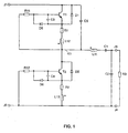
- FIG. 1 an embodiment of an inverter is shown.
- a DC voltage source can be connected to a first and a second DC voltage input J1 and J2.
- a positive pole of the DC voltage source must be connected to J1 and a negative pole to J2.
- a first series arrangement forms the series connection of a first electronic switch T1, a resistor R1 and a first secondary winding L12.
- a second series arrangement forms the series connection of a second electronic switch T2, a resistor R2 and a second secondary winding L13.
- the two series arrangements are connected in series and connected between the DC voltage inputs J1 and J2. Thus form the two series arrangements a half bridge.
- an AC output K1 At the connection point of the two series arrangements is an AC output K1.
- the potential of the AC output K1 is alternately at the potential of J1 and J2.
- the electronic switches are preferably designed as an NPN bipolar transistor.
- B. PNP bipolar transistor, MOSFET or IGBT possible.
- the resistors R1 and R2 are each a negative feedback for T1 and T2 with well known effect. They can also be omitted and replaced by a short circuit.
- the secondary winding L12 is connected to the emitter of T1 via the resistor R1.
- the secondary winding L12 is connected in series to the load resistance of T1.
- This series connection of the load resistor of T1 and the secondary winding L12 is connected between the DC voltage input J1 and the AC output K1.
- the secondary winding L13 is connected via the resistor R2 to the emitter of T2.
- the secondary winding L13 is connected in series to the load resistor of T2.
- This series connection of the load resistor of T2 and the secondary winding L13 is connected between the DC voltage input J2 and the AC output K1.
- a well-known freewheeling diode D1 and D2 is connected in each case. These diodes can also be integrated in the electronic switch or they can be dispensed with altogether.
- snubber capacitor C5 is connected between the AC voltage output K1 and the DC voltage input J1 . It reduces the edge steepness of the voltage at the AC output K1. C5 can also be connected to J2.
- the control of the electronic switch by the secondary windings L12 and L 13 is effective, the respective control contact is switched so that the respective control resistor and the respective secondary winding come to rest in a mesh.
- the base of T1 is connected via a resistor R11 to the AC voltage output K1
- the base of T2 is connected via a resistor R12 to the DC voltage input J2.
- a diode D5, D6 and a capacitor C3, C4 is connected in each case.
- the diodes D5, D6 and the capacitors C3, C4 are not mandatory. They serve to optimize the control of the electronic switches T1, T2.
- the circuit arrangement has two load outputs J3 and J4 to which a load can be connected.
- the potential of J4 can be understood as reference potential.
- J4 is connected to the DC input J2. It is also possible to connect J4 to J1 or by means of a voltage divider to provide a desired reference potential to which J4 is connected.
- a reactance network is connected, which transforms the impedance at the AC output K1 to the load outputs. It consists of the primary winding L11 and the capacitors C1 and C2. The primary winding L11 and the capacitor C1 are connected in series and connected between the AC output K1 and the load output J3. The capacitor C2 is connected between the load outputs J3 and J4.
- the primary winding L11 is coupled to the secondary windings L12 and L13.
- the primary winding L11 and the secondary windings L12 and L13 form a transformer.
- the respective Wickelsinn the transformer windings is characterized in a known manner by dots.
- the primary winding L11 is coupled to the AC output K1 at a first terminal and to the load terminal J3 at a second terminal.
- the primary winding L11 is traversed by a load current.
- a load resistor R3 is representatively connected to the load outputs J3 and J4 as representative of any loads.
- the reactance network can be modified in any way. Only the primary winding must, as described above, be traversed by a load current.
- This in FIG. 1 illustrated reactance network is preferably used in the case that one or more gas discharge lamps are connected for R3.
- C1 forms a blocking capacitor, which prevents the voltage between the load outputs J3 and J4 from having a DC component.
- the primary winding L11 takes over the task of a lamp inductor in this case and forms together with C2 a series resonant circuit.
- a load is coupled via a further winding on the transformer. It can also be a halogen incandescent lamp.
- the half bridge can also be extended to the full bridge.
- the primary winding is then connected in the bridge branch.
- the transformer then has two further secondary windings for the equivalent control of the two other electronic switches.
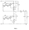
- FIG. 2 is shown a further embodiment of an inverter.
- FIG. 2 is compared with FIG. 1 connected in parallel to the resistors R11 and R12, respectively, the series circuit of a resistor R21 or R22 and a diode D21 and D22.
- the turning off of the electronic switches T1 and T2 is improved.
- FIG. 3 an embodiment of an inverter according to the invention is shown.
- the resistors R11 and R22 are replaced by a choke L31 and L32, respectively.
- a resistor R31 or R32 is connected in series with the diodes D5 and D6.
- FIG. 2 represent a further improvement of the switching on and off of T1 and T2. Mainly thereby switching losses are reduced and optimizes switching times with respect to the resonance characteristics of a load circuit consisting of reactance network and load.
- z. B. 30 kHz it has been found that the use of Schottky diodes for D5 and D6 and the short-circuiting of the resistors R31 and R32 has an advantageous effect on the power loss of the inverter.
- FIG. 3 Across from FIG. 2 has FIG. 3 following change:
- the capacitor C3 and the diode D1 are not as in FIG. 2 connected directly to the emitter of T1, but connected at the junction of R1 and the secondary winding L12.
- the connection of the capacitor C4 and the diode D2 is changed.
- the so-called free-wheeling current no longer flows through the resistor R1 or R2, whereby the efficiency of the circuit arrangement is improved.
- an improved switching behavior of the electronic switches T1, T2 is achieved by this change.
- a circuit arrangement according to the invention is used in an electronic operating device for the operation of fluorescent lamps.
- an operating device contains means for providing a DC voltage from an AC mains voltage. These may also include means for reducing line current harmonics.
- an operating device may include means that cause a control of operating parameters.
- such an operating device may include means that causes a shutdown of the operating device in abnormal operating conditions.
- such a control device may contain means that are suitable for suppressing radio interference.
Description
Die Erfindung betrifft Schaltungsanordnungen zum Erzeugen von Wechselspannung aus einer Gleichspannung. Es handelt sich dabei insbesondere um selbstschwingende Wechselrichter. Bevorzugtes Anwendungsgebiet derartiger Wechselrichter sind Betriebsgeräte für Gasentladungslampen.The invention relates to circuit arrangements for generating AC voltage from a DC voltage. These are in particular self-oscillating inverters. Preferred application of such inverters are control gear for gas discharge lamps.
Die erzeugte Wechselspannung bewirkt in einer angeschlossenen Last einen Wechselstrom. Auch die speisende Gleichspannung liefert einen Gleichstrom. Damit betrifft die Erfindung analog zu obiger Aussage auch Schaltungsanordnungen zum Erzeugen von Wechselstrom aus einem Gleichstrom. Ohne Einschränkung der Allgemeinheit werden im folgenden nur noch die Wechselspannung und die Gleichspannung beschrieben.The generated alternating voltage causes an alternating current in a connected load. The DC supply voltage also supplies a direct current. Thus, the invention relates analogous to the above statement, circuit arrangements for generating alternating current from a direct current. Without limiting the generality, only the AC voltage and the DC voltage will be described below.
Als Schaltungsanordnung zum Erzeugen von Wechselspannung aus einer Gleichspannung, im folgenden auch Wechselrichter genannt, sind Halb- und Vollbrückenschaltungen bekannt. Insbesondere zum Betrieb von Gasentladungslampen werden Halbbrückenschaltungen verwendet.As a circuit arrangement for generating AC voltage from a DC voltage, hereinafter also referred to as inverters, half and full bridge circuits are known. In particular, for the operation of gas discharge lamps half-bridge circuits are used.
Die Halbbrücke enthält zwei in Serie geschaltete elektronische Schalter, die abwechselnd ein- und ausgeschaltet werden. Die Ansteuerung dieser Schalter erfolgt entweder aus einer Steuerschaltung oder aus einem angeschlossenen Lastkreis. Im letzt genannten Fall erzeugt sich die Halbbrücke die Ansteuerung der elektronischen Schalter über Rückkoppelmittel selbst, weshalb eine derartige Schaltungsanordnung selbstschwingende Halbbrücke genannt wird. Für eine kostengünstige Realisierung eines Wechselrichters wird im Stand der Technik eine selbstschwingende Halbbrücke mit Bipolartransistoren verwendet. Dadurch wird die Steuerschaltung eingespart und der Einsatz kostengünstiger Bipolartransistoren wird ermöglicht.The half-bridge contains two series-connected electronic switches, which are alternately turned on and off. The activation of these switches takes place either from a control circuit or from a connected load circuit. In the latter case, the half-bridge generates the control of the electronic switch via feedback means itself, which is why such a circuit arrangement is called self-oscillating half-bridge. For a cost-effective implementation of an inverter, a self-oscillating half-bridge with bipolar transistors is used in the prior art. As a result, the control circuit is saved and the use of inexpensive bipolar transistors is made possible.
In der Schrift
Im allgemeinen besitzt ein elektronischer Schalter zwei Arbeitskontakte und einen Steuerkontakt. Zwischen den Arbeitskontakten kann ein Arbeitswiderstand definiert werden und zwischen einem Arbeitskontakt und dem Steuerkontakt kann ein Steuerwiderstand definiert werden. Bei einem Bipolartransistor in einer Halbbrücke bilden Emitter und Kollektor die Arbeitskontakte und die Basis den Steuerkontakt. Der Steuerwiderstand liegt zwischen Basis und Emitter. Bei einem MOSFET in einer Halbbrücke bilden Source und Drain die Arbeitskontakte und das Gate den Steuerkontakt. Der Steuerwiderstand liegt zwischen Gate und Source.In general, an electronic switch has two normally open contacts and a control contact. Between the normally open contacts a load resistor can be defined and between a normally open contact and the control contact a control resistor can be defined. In a bipolar transistor in a half-bridge emitter and collector form the normally open contacts and the base the control contact. The control resistor is located between base and emitter. In a MOSFET in a half-bridge, the source and drain form the normally open contacts and the gate the control contact. The control resistor is between gate and source.
Die Schrift
Alle aus diesem Stand der Technik bekannten Ausführungsformen besitzen Sekundärwicklungen, die parallel zum Steuerwiderstand geschaltet sind.All known from this prior art embodiments have secondary windings which are connected in parallel to the control resistor.
Die Ausführungsformen aus diesem Stand der Technik weisen folgende Nachteile auf:
- Ausführungsformen mit nicht sättigendem Übertrager weisen teilweise hohe Schaltverluste auf, weil nicht immer ein spannungsloses Einschalten der elektronischen Schalter gewährleistet ist. Außerdem treten teilweise hohe Ansteuerverluste auf, weil die Basisströme der elektronischen Schalter hohe Werte annehmen können.
- Embodiments with non-saturating transformer sometimes have high switching losses, because not always a voltage-free switching of the electronic switch is guaranteed. In addition, partly high drive losses occur because the base currents of the electronic switches can assume high values.
Ausführungsformen mit sättigendem Übertrager weisen hohe Verluste des Übertragers aufgrund seiner starken Aussteuerung auf. Zudem sind die Sättigungseigenschaften großen Exemplarstreuungen unterworfen. Dies bedingt ein aufwändiges Selektionsverfahren bei der Auswahl des Übertragers in der Massenfertigung.Embodiments with a saturating transformer have high losses of the transformer due to its high modulation. In addition, the saturation properties are subject to large specimen spreads. This requires a complex selection process in the selection of the transformer in mass production.
Aus
Es ist Aufgabe der vorliegenden Erfindung, eine Schaltungsanordnung zum Erzeugen von Wechselspannung aus einer Gleichspannung bereitzustellen, die kostengünstig und verlustarm ein Selbstschwingen mit Übertrager bewerkstelligt. Als kostengünstig wird eine Lösung auch dann erachtet, wenn sie keine Bauteile benötigt, die hohe Toleranzen mit sich bringen.It is an object of the present invention to provide a circuit arrangement for generating AC voltage from a DC voltage, which accomplishes cost-effective and low-loss self-oscillation with transformer. As a cost, a solution is considered even if it does not require components that bring high tolerances.
Diese Aufgabe wird ausgehend von den Merkmalen des Oberbegriffs des Patentanspruchs 1 durch seine kennzeichnenden Merkmale gelöst. Vorteilhafte Ausführumgsformen sind in den abhängigen Ansprüchen definiert.This object is achieved on the basis of the features of the preamble of patent claim 1 by its characterizing features. Advantageous embodiments are defined in the dependent claims.
Im folgenden soll die Erfindung anhand von Ausführungsbeispielen unter Bezugnahme auf Zeichnungen näher erläutert werden. Es zeigen:
- Figur 1
- ein Ausführungsbeispiel einer Schaltungsanordnung,
- Figur 2
- ein Ausführungsbeispiel in Anlehnung an
Figur 1 mit verbesserter Ansteuerung der elektronischen Schalter, - Figur 3
- ein Ausführungsbeispiel in Anlehnung an
Figur 1 mit erfindungsgemäß verbesserter Ansteuerung der elektronischen Schalter,
- FIG. 1
- an embodiment of a circuit arrangement,
- FIG. 2
- an embodiment in accordance with
FIG. 1 with improved control of the electronic switches, - FIG. 3
- an embodiment in accordance with
FIG. 1 with inventively improved control of the electronic switch,
Im folgenden werden Widerstände durch den Buchstaben R, Kondensatoren durch den Buchstaben C, Transistoren durch den Buchstaben T, Dioden durch den Buchstaben D, Verbindungsstellen durch den Buchstaben J jeweils gefolgt von einer Zahl bezeichnet. Auch werden im folgenden für gleiche und gleichwirkende Elemente der verschiedenen Ausführungsbeispiele durchweg gleiche Bezugszeichen verwendet.In the following, resistors are denoted by the letter R, capacitors by the letter C, transistors by the letter T, diodes by the letter D, joints by the letter J each followed by a number. Also, the same reference numerals are used throughout for the same and equivalent elements of the various embodiments.
In
An einem ersten und einem zweiten Gleichspannungseingang J1 und J2 ist eine Gleichspannungsquelle anschließbar. Im vorliegenden Beispiel muss ein Pluspol der Gleichspannungsquelle an J1 und ein Minuspol an J2 angeschlossen werden.A DC voltage source can be connected to a first and a second DC voltage input J1 and J2. In the present example, a positive pole of the DC voltage source must be connected to J1 and a negative pole to J2.
Eine erste Serienanordnung bildet die Serienschaltung aus einem ersten elektronischen Schalter T1, einem Widerstand R1 und einer ersten Sekundärwicklung L12.A first series arrangement forms the series connection of a first electronic switch T1, a resistor R1 and a first secondary winding L12.
Eine zweite Serienanordnung bildet die Serienschaltung aus einem zweiten elektronischen Schalter T2, einem Widerstand R2 und einer zweiten Sekundärwicklung L13.A second series arrangement forms the series connection of a second electronic switch T2, a resistor R2 and a second secondary winding L13.
Die beiden Serienanordnungen sind in Serie geschaltet und zwischen die Gleichspannungseingänge J1 und J2 geschaltet. Damit bilden die beiden Serienanordnungen eine Halbbrücke. Am Verbindungspunkt der beiden Serienanordnungen befindet sich ein Wechselspannungsausgang K1. Durch abwechselndes Einschalten der elektronischen Schalter befindet sich das Potenzial des Wechselspannungsausgangs K1 abwechselnd auf dem Potenzial von J1 und J2.The two series arrangements are connected in series and connected between the DC voltage inputs J1 and J2. Thus form the two series arrangements a half bridge. At the connection point of the two series arrangements is an AC output K1. By alternately turning on the electronic switches, the potential of the AC output K1 is alternately at the potential of J1 and J2.
Aus Kostengründen sind die elektronischen Schalter bevorzugt als NPN Bipolartransistor ausgeführt. Es sind jedoch auch andere elektronischen Schalter wie z. B. PNP Bipolartransistor, MOSFET oder IGBT möglich.For cost reasons, the electronic switches are preferably designed as an NPN bipolar transistor. However, there are other electronic switches such. B. PNP bipolar transistor, MOSFET or IGBT possible.
Die Widerstände R1 und R2 dienen jeweils einer Gegenkopplung für T1 und T2 mit allgemein bekannter Wirkung. Sie können auch entfallen und durch einen Kurzschluss ersetzt werden.The resistors R1 and R2 are each a negative feedback for T1 and T2 with well known effect. They can also be omitted and replaced by a short circuit.
Wichtig für die Wirkung der Sekundärwicklungen L12 und L13 ist deren Anordnung bezüglich der Anschlüsse der elektronischen Schalter. Im Ausführungsbeispiel nach
Parallel zu den Arbeitswiderständen von T1 und T2 ist jeweils eine allgemein bekannte Freilaufdiode D1 und D2 geschaltet. Diese Dioden können auch im elektronischen Schalter integriert sein oder sie können ganz entfallen.Parallel to the load resistors of T1 and T2, a well-known freewheeling diode D1 and D2 is connected in each case. These diodes can also be integrated in the electronic switch or they can be dispensed with altogether.
Zwischen dem Wechselspannungsausgang K1 und dem Gleichspannungseingang J1 ist ein so genannter Snubber-Kondensator C5 geschaltet. Er reduziert die Flankensteilheit der Spannung am Wechselspannungsausgang K1. C5 kann auch mit J2 verbunden sein.Between the AC voltage output K1 and the DC voltage input J1 a so-called snubber capacitor C5 is connected. It reduces the edge steepness of the voltage at the AC output K1. C5 can also be connected to J2.
Damit die Ansteuerung der elektronischen Schalter durch die Sekundärwicklungen L12 und L 13 wirksam ist, ist der jeweilige Steuerkontakt so geschaltet, dass der jeweilige Steuerwiderstand und die jeweilige Sekundärwicklung in einer Masche zu liegen kommen. Dazu ist die Basis von T1 über einen Widerstand R11 mit dem Wechselspannungsausgang K1 verbunden und die Basis von T2 über einen Widerstand R12 mit dem Gleichspannungseingang J2 verbunden.Thus, the control of the electronic switch by the secondary windings L12 and L 13 is effective, the respective control contact is switched so that the respective control resistor and the respective secondary winding come to rest in a mesh. For this purpose, the base of T1 is connected via a resistor R11 to the AC voltage output K1, and the base of T2 is connected via a resistor R12 to the DC voltage input J2.
Parallel zu den Steuerwiderständen von T1 und T2 ist jeweils eine Diode D5, D6 und ein Kondensator C3, C4 geschaltet. Die Dioden D5, D6 und die Kondensatoren C3, C4 sind nicht zwingend erforderlich. Sie dienen zur Optimierung der Ansteueerung der ektronischen Schalter T1, T2.Parallel to the control resistors of T1 and T2, a diode D5, D6 and a capacitor C3, C4 is connected in each case. The diodes D5, D6 and the capacitors C3, C4 are not mandatory. They serve to optimize the control of the electronic switches T1, T2.
Die Schaltungsanordnung besitzt zwei Lastausgänge J3 und J4 an denen einen Last anschließbar ist. Das Potenzial an J4 kann als Bezugspotenzial aufgefasst werden. J4 ist mit dem Gleichspannungseingang J2 verbunden. Es ist auch möglich J4 mit J1 zu verbinden oder mittels eines Spannungsteilers ein gewünschtes Bezugspotenzial zuschaffen, mit dem J4 verbunden ist.The circuit arrangement has two load outputs J3 and J4 to which a load can be connected. The potential of J4 can be understood as reference potential. J4 is connected to the DC input J2. It is also possible to connect J4 to J1 or by means of a voltage divider to provide a desired reference potential to which J4 is connected.
Zwischen dem Wechselspannungsausgang K1 und den Lastausgängen J3, J4 ist ein Reaktanznetzwerk geschaltet, das die Impedanz am Wechselspannungsausgang K1 zu den Lastausgängen hin transformiert. Es besteht aus der Primärwicklung L11 und den Kondensatoren C1 und C2. Die Primärwicklung L11 und der Kondensator C1 sind in Serie geschaltet und zwischen den Wechselspannungsausgang K1 und den Lastausgang J3 geschaltet. Der Kondensator C2 ist zwischen die Lastausgänge J3 und J4 geschaltet.Between the AC output K1 and the load outputs J3, J4, a reactance network is connected, which transforms the impedance at the AC output K1 to the load outputs. It consists of the primary winding L11 and the capacitors C1 and C2. The primary winding L11 and the capacitor C1 are connected in series and connected between the AC output K1 and the load output J3. The capacitor C2 is connected between the load outputs J3 and J4.
Die Primärwicklung L11 ist mit den Sekundärwicklungen L12 und L13 gekoppelt. Somit bilden die Primärwicklung L11 und die Sekundärwicklungen L12 und L13 einen Übertrager. Der jeweilige Wickelsinn der Übertragerwicklungen ist in bekannter Weise durch Punkte gekennzeichnet. Die Primärwicklung L11 ist mit einem ersten Anschluss mit dem Wechselspannungsausgang K1 und mit einem zweiten Anschluss mit dem Lastausgang J3 gekoppelt. Damit wird die Primärwicklung L11 von einem Laststrom durchflossen.The primary winding L11 is coupled to the secondary windings L12 and L13. Thus, the primary winding L11 and the secondary windings L12 and L13 form a transformer. The respective Wickelsinn the transformer windings is characterized in a known manner by dots. The primary winding L11 is coupled to the AC output K1 at a first terminal and to the load terminal J3 at a second terminal. Thus, the primary winding L11 is traversed by a load current.
An die Lastausgänge J3 und J4 ist repräsentativ für beliebige Lasten ein Lastwiderstand R3 geschaltet. Das Reaktanznetzwerk kann in beliebiger Weise modifiziert werden. Lediglich die Primärwicklung muss, wie oben beschrieben von einem Laststrom durchflossen sein. Das in
Es ist auch möglich, dass eine Last über eine weitere Wicklung auf dem Übertrager angekoppelt wird. Dabei kann es sich auch um eine Halogenglühlampe handeln.It is also possible that a load is coupled via a further winding on the transformer. It can also be a halogen incandescent lamp.
Die Halbbrücke kann auch zur Vollbrücke erweitert werden. Die Primärwicklung ist dann in den Brückezweig geschaltet. Außerdem weist der Übertrager dann zwei weitere Sekundärwicklungen zur äquivalenten Ansteuerung der beiden weiteren elektronischen Schalter auf.The half bridge can also be extended to the full bridge. The primary winding is then connected in the bridge branch. In addition, the transformer then has two further secondary windings for the equivalent control of the two other electronic switches.
In
In
Gegenüber
Die im folgenden angegebene Dimensionierung von wesentlichen Bauelementen aus
- Übertragerkern: EVD 25
- L11: 128 Windungen
- L12: 4 Windungen
- L 13: 4 Windungen
- C2: 12nF
- R1, R2: 1Ohm
- L31, L32: 1mH
- R21, R22: 39 Ohm
- R31, R32: 4,7 Ohm
- Carrier core: EVD 25
- L11: 128 turns
- L12: 4 turns
- L 13: 4 turns
- C2: 12nF
- R1, R2: 1 ohm
- L31, L32: 1mH
- R21, R22: 39 ohms
- R31, R32: 4.7 ohms
Es ergibt sich eine Schwingfrequenz des Wechselrichters von ca. 50 kHz. Beim Einsatz von Bipolartransistoren ist ein Betrieb im Frequenzbereich zwischen 20 KHz und 100 kHz vorteilhaft.This results in an oscillation frequency of the inverter of about 50 kHz. When using bipolar transistors, operation in the frequency range between 20 kHz and 100 kHz is advantageous.
Bevorzugt wird eine erfindungsgemäße Schaltungsanordnung in einem elektronischen Betriebsgerät zum Betrieb von Leuchtstofflampen eingesetzt. Zusätzlich zur erfindungsgemäßen Schaltungsanordnung enthält ein derartiges Betriebsgerät Mittel zum Bereitstellen einer Gleichspannung aus einer Netzwechselspannung. Diese können auch Mittel zur Reduzierung der Netzstromoberschwingungen enthalten. Weiterhin kann ein derartiges Betriebsgerät Mittel enthalten, die eine Regelung von Betriebsparametern bewirken. Weiterhin kann ein derartiges Betriebsgerät Mittel enthalten, die eine Abschaltung des Betriebsgeräts bei anormalen Betriebszuständen bewirkt. Weiterhin kann ein derartiges Betriebsgerät Mittel enthalten, die zur Unterdrückung von Funkstörungen geeignet sind.Preferably, a circuit arrangement according to the invention is used in an electronic operating device for the operation of fluorescent lamps. In addition to the circuit arrangement according to the invention, such an operating device contains means for providing a DC voltage from an AC mains voltage. These may also include means for reducing line current harmonics. Furthermore, such an operating device may include means that cause a control of operating parameters. Furthermore, such an operating device may include means that causes a shutdown of the operating device in abnormal operating conditions. Furthermore, such a control device may contain means that are suitable for suppressing radio interference.
Claims (4)
- Circuit arrangement for generating an AC voltage having the following features:• a first and a second DC voltage input (J1, J2), to which a DC voltage source may be connected,• at least one AC voltage output (K1),• at least one load output (J3, J4), to which a load (R3) may be connected,• two electronic switches (T1, T2) each having two make contacts and a control contact, as a result of which a load resistor is defined between the make contacts, and a control resistor is defined between the control contact and a make contact,• a make contact is coupled to a DC voltage input (J1, J2), and the other make contact is coupled to the AC voltage output (K1),• a transformer having a primary (L11) and at least one secondary winding (L12, L13), a first terminal of the primary winding being coupled to the AC voltage output (K1), and a second terminal of the primary winding being coupled to the load output (J3),• the at least one secondary winding (L12, L13) and the load resistor form a series circuit which is connected between a DC voltage input (J1, J2) and the AC voltage output (K1),• the control contact is connected such that the control resistor and the at least one secondary winding (L12, L13) are in a mesh,• the two electronic switches (T1, T2) are arranged in a half-bridge circuit,• the load resistors of the two electronic switches (T1, T2) are each connected in series with a secondary winding (L12, L13),characterized in that the control resistors of the electronic switches (T1, T2) and the secondary windings (L12, L13) are each connected via an inductor (L31, L32) to form a mesh.
- The circuit arrangement as claimed in claim 1,
characterized in that the electronic switches (T1, T2) are in the form of bipolar transistors. - The circuit arrangement as claimed in claim 1 or 2,
characterized in that in each case the series circuit comprising a diode (D21, D22) and a resistor (R21, R22) is connected in parallel with the inductors (L31, L32). - An operating device for operating fluorescent lamps,
characterized in that the operating device comprises a circuit arrangement as claimed in one of claims 1 to 3.
Applications Claiming Priority (2)
| Application Number | Priority Date | Filing Date | Title |
|---|---|---|---|
| DE10343275A DE10343275A1 (en) | 2003-09-18 | 2003-09-18 | Circuit arrangement for generating AC voltage from a DC voltage |
| DE10343275 | 2003-09-18 |
Publications (3)
| Publication Number | Publication Date |
|---|---|
| EP1517592A2 EP1517592A2 (en) | 2005-03-23 |
| EP1517592A3 EP1517592A3 (en) | 2008-01-16 |
| EP1517592B1 true EP1517592B1 (en) | 2016-09-28 |
Family
ID=34177819
Family Applications (1)
| Application Number | Title | Priority Date | Filing Date |
|---|---|---|---|
| EP04019087.8A Not-in-force EP1517592B1 (en) | 2003-09-18 | 2004-08-11 | Circuitry for the generation of an AC voltage from a DC voltage |
Country Status (8)
| Country | Link |
|---|---|
| US (1) | US7030566B2 (en) |
| EP (1) | EP1517592B1 (en) |
| KR (1) | KR101029174B1 (en) |
| CN (1) | CN100472929C (en) |
| CA (1) | CA2481537A1 (en) |
| DE (1) | DE10343275A1 (en) |
| RU (1) | RU2339151C2 (en) |
| TW (1) | TW200524261A (en) |
Families Citing this family (3)
| Publication number | Priority date | Publication date | Assignee | Title |
|---|---|---|---|---|
| US7545963B2 (en) * | 2003-04-04 | 2009-06-09 | Lumidigm, Inc. | Texture-biometrics sensor |
| US7560874B2 (en) * | 2006-09-30 | 2009-07-14 | Osram Sylvania Inc. | Electronic ballast with improved inverter startup circuit |
| WO2009076769A1 (en) * | 2007-12-17 | 2009-06-25 | The University Of British Columbia | A method and system for protecting an electrical power transmission network |
Family Cites Families (10)
| Publication number | Priority date | Publication date | Assignee | Title |
|---|---|---|---|---|
| US3117289A (en) * | 1961-08-07 | 1964-01-07 | Automatic Elect Lab | Transistor tone generator |
| US3922582A (en) * | 1974-08-22 | 1975-11-25 | Gte Sylvania Inc | Current limited oxcillator arrangement |
| KR900002446B1 (en) * | 1986-05-30 | 1990-04-14 | 가부시끼 가이샤 도시바 | Inacrive gas discharge lamp device |
| DE3829388A1 (en) * | 1988-08-30 | 1990-03-01 | Patent Treuhand Ges Fuer Elektrische Gluehlampen Mbh | CIRCUIT ARRANGEMENT FOR OPERATING A LOAD |
| FR2700426A1 (en) * | 1993-01-08 | 1994-07-13 | Courier De Mere Henri Edouard | High capacity transistor-based electric energy converter ensuring correct supply to e.g. fluorescent lamp electronic ballast |
| JP3382012B2 (en) | 1994-04-25 | 2003-03-04 | 松下電工株式会社 | Self-excited inverter device |
| DE4430397A1 (en) * | 1994-08-26 | 1996-02-29 | Patent Treuhand Ges Fuer Elektrische Gluehlampen Mbh | Circuit arrangement for operating low-pressure discharge lamps |
| US5898278A (en) * | 1995-08-09 | 1999-04-27 | Pinbeam Ag | Series resonant lamp circuit having direct electrode connection between rectifier and AC source |
| DE19905487A1 (en) * | 1999-02-11 | 2000-08-31 | Patent Treuhand Ges Fuer Elektrische Gluehlampen Mbh | Circuit arrangement for operating at least one low-pressure discharge lamp |
| WO2002047441A1 (en) * | 2000-12-04 | 2002-06-13 | Koninklijke Philips Electronics N.V. | Ballast circuit arrangement |
-
2003
- 2003-09-18 DE DE10343275A patent/DE10343275A1/en not_active Withdrawn
-
2004
- 2004-08-11 TW TW093123990A patent/TW200524261A/en unknown
- 2004-08-11 EP EP04019087.8A patent/EP1517592B1/en not_active Not-in-force
- 2004-09-08 US US10/935,223 patent/US7030566B2/en active Active
- 2004-09-13 KR KR1020040072943A patent/KR101029174B1/en not_active IP Right Cessation
- 2004-09-14 CA CA002481537A patent/CA2481537A1/en not_active Abandoned
- 2004-09-17 CN CNB2004100787687A patent/CN100472929C/en not_active Expired - Fee Related
- 2004-09-17 RU RU2004127897/09A patent/RU2339151C2/en not_active IP Right Cessation
Also Published As
| Publication number | Publication date |
|---|---|
| US7030566B2 (en) | 2006-04-18 |
| CA2481537A1 (en) | 2005-03-18 |
| CN100472929C (en) | 2009-03-25 |
| EP1517592A2 (en) | 2005-03-23 |
| RU2004127897A (en) | 2006-02-20 |
| CN1599224A (en) | 2005-03-23 |
| DE10343275A1 (en) | 2005-05-12 |
| TW200524261A (en) | 2005-07-16 |
| KR20050028309A (en) | 2005-03-22 |
| EP1517592A3 (en) | 2008-01-16 |
| KR101029174B1 (en) | 2011-04-12 |
| US20050062438A1 (en) | 2005-03-24 |
| RU2339151C2 (en) | 2008-11-20 |
Similar Documents
| Publication | Publication Date | Title |
|---|---|---|
| EP0264765B1 (en) | Circuit arrangement for operating low-voltage halogen incandescent lamps | |
| EP1638374B1 (en) | Circuit arrangement for operating at least a light source with improved crest factor | |
| EP1710898B1 (en) | Switchable voltage converter | |
| EP0781077A2 (en) | Circuit for operating a lamp | |
| CH657003A5 (en) | CONTROL UNIT FOR OPERATING AT LEAST ONE LOW PRESSURE DISCHARGE LAMP. | |
| EP2852044B1 (en) | Bidirectional converter with preferred direction and inverter with reactive power capability | |
| EP0982862B1 (en) | Bipolar bridge circuit without resistors | |
| EP0917412A2 (en) | Self-oscillating circuit with simplified startup circuit | |
| DE10062047A1 (en) | Electronic transformer with good immunity to high voltage pulses | |
| WO2009010098A1 (en) | Circuit arrangement comprising a voltage transformer and associated method | |
| DE10241327A1 (en) | Circuit arrangement for operating discharge lamps | |
| EP1553810B1 (en) | Circuit arrangement for operating light sources with power factor correction | |
| EP1517592B1 (en) | Circuitry for the generation of an AC voltage from a DC voltage | |
| EP1326484B1 (en) | Apparatus for operating discharge lamps | |
| EP1608208B1 (en) | Circuit with shut-down device for operating light sources | |
| EP1615476B1 (en) | Full-bridge circuit for operating discharge lamps, with means for relieving the switches of said full-bridge circuit | |
| EP1429461A1 (en) | Switching power supply | |
| DE4329821A1 (en) | Electronic ballast for supplying a load, for example a lamp | |
| EP0992113B1 (en) | Half bridge circuit drive without collector bias current peak | |
| DE20316196U1 (en) | Free-running inverter circuit e.g. for driving florescent lamp, has control contact connected so that respective control resistance lies in mesh with respective secondary winding | |
| DE4436465A1 (en) | Circuit arrangement for operating incandescent lamps | |
| DE10220471A1 (en) | Circuit arrangement for operating discharge lamps | |
| EP2140735B1 (en) | Circuit configuration for starting and operating at least one discharge lamp | |
| EP1553811A2 (en) | Circuit arrangement for operating light sources with power factor correction | |
| DE102004031445A1 (en) | Circuit arrangement and operating device for operating lamps |
Legal Events
| Date | Code | Title | Description |
|---|---|---|---|
| PUAI | Public reference made under article 153(3) epc to a published international application that has entered the european phase |
Free format text: ORIGINAL CODE: 0009012 |
|
| AK | Designated contracting states |
Kind code of ref document: A2 Designated state(s): AT BE BG CH CY CZ DE DK EE ES FI FR GB GR HU IE IT LI LU MC NL PL PT RO SE SI SK TR |
|
| AX | Request for extension of the european patent |
Extension state: AL HR LT LV MK |
|
| PUAL | Search report despatched |
Free format text: ORIGINAL CODE: 0009013 |
|
| AK | Designated contracting states |
Kind code of ref document: A3 Designated state(s): AT BE BG CH CY CZ DE DK EE ES FI FR GB GR HU IE IT LI LU MC NL PL PT RO SE SI SK TR |
|
| AX | Request for extension of the european patent |
Extension state: AL HR LT LV MK |
|
| 17P | Request for examination filed |
Effective date: 20080220 |
|
| AKX | Designation fees paid |
Designated state(s): AT BE BG CH CY CZ DE DK EE ES FI FR GB GR HU IE IT LI LU MC NL PL PT RO SE SI SK TR |
|
| RAP1 | Party data changed (applicant data changed or rights of an application transferred) |
Owner name: OSRAM SYLVANIA INC. |
|
| 17Q | First examination report despatched |
Effective date: 20151223 |
|
| REG | Reference to a national code |
Ref country code: DE Ref legal event code: R079 Ref document number: 502004015321 Country of ref document: DE Free format text: PREVIOUS MAIN CLASS: H05B0041280000 Ipc: H02M0007538300 |
|
| RIC1 | Information provided on ipc code assigned before grant |
Ipc: H02M 7/5383 20070101AFI20160307BHEP |
|
| GRAP | Despatch of communication of intention to grant a patent |
Free format text: ORIGINAL CODE: EPIDOSNIGR1 |
|
| INTG | Intention to grant announced |
Effective date: 20160421 |
|
| GRAS | Grant fee paid |
Free format text: ORIGINAL CODE: EPIDOSNIGR3 |
|
| GRAA | (expected) grant |
Free format text: ORIGINAL CODE: 0009210 |
|
| AK | Designated contracting states |
Kind code of ref document: B1 Designated state(s): AT BE BG CH CY CZ DE DK EE ES FI FR GB GR HU IE IT LI LU MC NL PL PT RO SE SI SK TR |
|
| REG | Reference to a national code |
Ref country code: GB Ref legal event code: FG4D Free format text: NOT ENGLISH |
|
| REG | Reference to a national code |
Ref country code: CH Ref legal event code: EP |
|
| REG | Reference to a national code |
Ref country code: AT Ref legal event code: REF Ref document number: 833509 Country of ref document: AT Kind code of ref document: T Effective date: 20161015 |
|
| REG | Reference to a national code |
Ref country code: IE Ref legal event code: FG4D Free format text: LANGUAGE OF EP DOCUMENT: GERMAN |
|
| REG | Reference to a national code |
Ref country code: DE Ref legal event code: R096 Ref document number: 502004015321 Country of ref document: DE |
|
| PG25 | Lapsed in a contracting state [announced via postgrant information from national office to epo] |
Ref country code: FI Free format text: LAPSE BECAUSE OF FAILURE TO SUBMIT A TRANSLATION OF THE DESCRIPTION OR TO PAY THE FEE WITHIN THE PRESCRIBED TIME-LIMIT Effective date: 20160928 |
|
| REG | Reference to a national code |
Ref country code: NL Ref legal event code: MP Effective date: 20160928 |
|
| PG25 | Lapsed in a contracting state [announced via postgrant information from national office to epo] |
Ref country code: NL Free format text: LAPSE BECAUSE OF FAILURE TO SUBMIT A TRANSLATION OF THE DESCRIPTION OR TO PAY THE FEE WITHIN THE PRESCRIBED TIME-LIMIT Effective date: 20160928 Ref country code: SE Free format text: LAPSE BECAUSE OF FAILURE TO SUBMIT A TRANSLATION OF THE DESCRIPTION OR TO PAY THE FEE WITHIN THE PRESCRIBED TIME-LIMIT Effective date: 20160928 Ref country code: GR Free format text: LAPSE BECAUSE OF FAILURE TO SUBMIT A TRANSLATION OF THE DESCRIPTION OR TO PAY THE FEE WITHIN THE PRESCRIBED TIME-LIMIT Effective date: 20161229 |
|
| PG25 | Lapsed in a contracting state [announced via postgrant information from national office to epo] |
Ref country code: RO Free format text: LAPSE BECAUSE OF FAILURE TO SUBMIT A TRANSLATION OF THE DESCRIPTION OR TO PAY THE FEE WITHIN THE PRESCRIBED TIME-LIMIT Effective date: 20160928 Ref country code: EE Free format text: LAPSE BECAUSE OF FAILURE TO SUBMIT A TRANSLATION OF THE DESCRIPTION OR TO PAY THE FEE WITHIN THE PRESCRIBED TIME-LIMIT Effective date: 20160928 |
|
| PG25 | Lapsed in a contracting state [announced via postgrant information from national office to epo] |
Ref country code: CZ Free format text: LAPSE BECAUSE OF FAILURE TO SUBMIT A TRANSLATION OF THE DESCRIPTION OR TO PAY THE FEE WITHIN THE PRESCRIBED TIME-LIMIT Effective date: 20160928 Ref country code: ES Free format text: LAPSE BECAUSE OF FAILURE TO SUBMIT A TRANSLATION OF THE DESCRIPTION OR TO PAY THE FEE WITHIN THE PRESCRIBED TIME-LIMIT Effective date: 20160928 Ref country code: PL Free format text: LAPSE BECAUSE OF FAILURE TO SUBMIT A TRANSLATION OF THE DESCRIPTION OR TO PAY THE FEE WITHIN THE PRESCRIBED TIME-LIMIT Effective date: 20160928 Ref country code: PT Free format text: LAPSE BECAUSE OF FAILURE TO SUBMIT A TRANSLATION OF THE DESCRIPTION OR TO PAY THE FEE WITHIN THE PRESCRIBED TIME-LIMIT Effective date: 20170130 Ref country code: BG Free format text: LAPSE BECAUSE OF FAILURE TO SUBMIT A TRANSLATION OF THE DESCRIPTION OR TO PAY THE FEE WITHIN THE PRESCRIBED TIME-LIMIT Effective date: 20161228 Ref country code: SK Free format text: LAPSE BECAUSE OF FAILURE TO SUBMIT A TRANSLATION OF THE DESCRIPTION OR TO PAY THE FEE WITHIN THE PRESCRIBED TIME-LIMIT Effective date: 20160928 |
|
| REG | Reference to a national code |
Ref country code: DE Ref legal event code: R097 Ref document number: 502004015321 Country of ref document: DE |
|
| PG25 | Lapsed in a contracting state [announced via postgrant information from national office to epo] |
Ref country code: IT Free format text: LAPSE BECAUSE OF FAILURE TO SUBMIT A TRANSLATION OF THE DESCRIPTION OR TO PAY THE FEE WITHIN THE PRESCRIBED TIME-LIMIT Effective date: 20160928 |
|
| PG25 | Lapsed in a contracting state [announced via postgrant information from national office to epo] |
Ref country code: DK Free format text: LAPSE BECAUSE OF FAILURE TO SUBMIT A TRANSLATION OF THE DESCRIPTION OR TO PAY THE FEE WITHIN THE PRESCRIBED TIME-LIMIT Effective date: 20160928 |
|
| PLBE | No opposition filed within time limit |
Free format text: ORIGINAL CODE: 0009261 |
|
| STAA | Information on the status of an ep patent application or granted ep patent |
Free format text: STATUS: NO OPPOSITION FILED WITHIN TIME LIMIT |
|
| REG | Reference to a national code |
Ref country code: FR Ref legal event code: PLFP Year of fee payment: 14 |
|
| 26N | No opposition filed |
Effective date: 20170629 |
|
| PG25 | Lapsed in a contracting state [announced via postgrant information from national office to epo] |
Ref country code: SI Free format text: LAPSE BECAUSE OF FAILURE TO SUBMIT A TRANSLATION OF THE DESCRIPTION OR TO PAY THE FEE WITHIN THE PRESCRIBED TIME-LIMIT Effective date: 20160928 |
|
| REG | Reference to a national code |
Ref country code: CH Ref legal event code: PL |
|
| PG25 | Lapsed in a contracting state [announced via postgrant information from national office to epo] |
Ref country code: MC Free format text: LAPSE BECAUSE OF FAILURE TO SUBMIT A TRANSLATION OF THE DESCRIPTION OR TO PAY THE FEE WITHIN THE PRESCRIBED TIME-LIMIT Effective date: 20160928 |
|
| PG25 | Lapsed in a contracting state [announced via postgrant information from national office to epo] |
Ref country code: LI Free format text: LAPSE BECAUSE OF NON-PAYMENT OF DUE FEES Effective date: 20170831 Ref country code: CH Free format text: LAPSE BECAUSE OF NON-PAYMENT OF DUE FEES Effective date: 20170831 |
|
| REG | Reference to a national code |
Ref country code: IE Ref legal event code: MM4A |
|
| REG | Reference to a national code |
Ref country code: BE Ref legal event code: MM Effective date: 20170831 |
|
| PG25 | Lapsed in a contracting state [announced via postgrant information from national office to epo] |
Ref country code: LU Free format text: LAPSE BECAUSE OF NON-PAYMENT OF DUE FEES Effective date: 20170811 |
|
| PG25 | Lapsed in a contracting state [announced via postgrant information from national office to epo] |
Ref country code: IE Free format text: LAPSE BECAUSE OF NON-PAYMENT OF DUE FEES Effective date: 20170811 |
|
| REG | Reference to a national code |
Ref country code: FR Ref legal event code: PLFP Year of fee payment: 15 |
|
| PG25 | Lapsed in a contracting state [announced via postgrant information from national office to epo] |
Ref country code: BE Free format text: LAPSE BECAUSE OF NON-PAYMENT OF DUE FEES Effective date: 20170831 |
|
| REG | Reference to a national code |
Ref country code: AT Ref legal event code: MM01 Ref document number: 833509 Country of ref document: AT Kind code of ref document: T Effective date: 20170811 |
|
| PGFP | Annual fee paid to national office [announced via postgrant information from national office to epo] |
Ref country code: DE Payment date: 20180823 Year of fee payment: 15 Ref country code: FR Payment date: 20180827 Year of fee payment: 15 |
|
| PG25 | Lapsed in a contracting state [announced via postgrant information from national office to epo] |
Ref country code: AT Free format text: LAPSE BECAUSE OF NON-PAYMENT OF DUE FEES Effective date: 20170811 |
|
| PGFP | Annual fee paid to national office [announced via postgrant information from national office to epo] |
Ref country code: GB Payment date: 20180822 Year of fee payment: 15 |
|
| PG25 | Lapsed in a contracting state [announced via postgrant information from national office to epo] |
Ref country code: HU Free format text: LAPSE BECAUSE OF FAILURE TO SUBMIT A TRANSLATION OF THE DESCRIPTION OR TO PAY THE FEE WITHIN THE PRESCRIBED TIME-LIMIT; INVALID AB INITIO Effective date: 20040811 |
|
| PG25 | Lapsed in a contracting state [announced via postgrant information from national office to epo] |
Ref country code: CY Free format text: LAPSE BECAUSE OF NON-PAYMENT OF DUE FEES Effective date: 20160928 |
|
| REG | Reference to a national code |
Ref country code: DE Ref legal event code: R119 Ref document number: 502004015321 Country of ref document: DE |
|
| PG25 | Lapsed in a contracting state [announced via postgrant information from national office to epo] |
Ref country code: TR Free format text: LAPSE BECAUSE OF FAILURE TO SUBMIT A TRANSLATION OF THE DESCRIPTION OR TO PAY THE FEE WITHIN THE PRESCRIBED TIME-LIMIT Effective date: 20160928 |
|
| GBPC | Gb: european patent ceased through non-payment of renewal fee |
Effective date: 20190811 |
|
| PG25 | Lapsed in a contracting state [announced via postgrant information from national office to epo] |
Ref country code: DE Free format text: LAPSE BECAUSE OF NON-PAYMENT OF DUE FEES Effective date: 20200303 Ref country code: FR Free format text: LAPSE BECAUSE OF NON-PAYMENT OF DUE FEES Effective date: 20190831 |
|
| PG25 | Lapsed in a contracting state [announced via postgrant information from national office to epo] |
Ref country code: GB Free format text: LAPSE BECAUSE OF NON-PAYMENT OF DUE FEES Effective date: 20190811 |