EP1517364A1 - Semiconductor device and its producing method - Google Patents
Semiconductor device and its producing method Download PDFInfo
- Publication number
- EP1517364A1 EP1517364A1 EP02738780A EP02738780A EP1517364A1 EP 1517364 A1 EP1517364 A1 EP 1517364A1 EP 02738780 A EP02738780 A EP 02738780A EP 02738780 A EP02738780 A EP 02738780A EP 1517364 A1 EP1517364 A1 EP 1517364A1
- Authority
- EP
- European Patent Office
- Prior art keywords
- pad electrode
- film
- electrode
- semiconductor device
- forming
- Prior art date
- Legal status (The legal status is an assumption and is not a legal conclusion. Google has not performed a legal analysis and makes no representation as to the accuracy of the status listed.)
- Granted
Links
Images



Classifications
-
- H—ELECTRICITY
- H10—SEMICONDUCTOR DEVICES; ELECTRIC SOLID-STATE DEVICES NOT OTHERWISE PROVIDED FOR
- H10P—GENERIC PROCESSES OR APPARATUS FOR THE MANUFACTURE OR TREATMENT OF DEVICES COVERED BY CLASS H10
- H10P14/00—Formation of materials, e.g. in the shape of layers or pillars
- H10P14/40—Formation of materials, e.g. in the shape of layers or pillars of conductive or resistive materials
- H10P14/46—Formation of materials, e.g. in the shape of layers or pillars of conductive or resistive materials using a liquid
- H10P14/47—Electrolytic deposition, i.e. electroplating; Electroless plating
-
- H—ELECTRICITY
- H10—SEMICONDUCTOR DEVICES; ELECTRIC SOLID-STATE DEVICES NOT OTHERWISE PROVIDED FOR
- H10W—GENERIC PACKAGES, INTERCONNECTIONS, CONNECTORS OR OTHER CONSTRUCTIONAL DETAILS OF DEVICES COVERED BY CLASS H10
- H10W42/00—Arrangements for protection of devices
- H10W42/121—Arrangements for protection of devices protecting against mechanical damage
-
- H—ELECTRICITY
- H10—SEMICONDUCTOR DEVICES; ELECTRIC SOLID-STATE DEVICES NOT OTHERWISE PROVIDED FOR
- H10W—GENERIC PACKAGES, INTERCONNECTIONS, CONNECTORS OR OTHER CONSTRUCTIONAL DETAILS OF DEVICES COVERED BY CLASS H10
- H10W72/00—Interconnections or connectors in packages
- H10W72/01—Manufacture or treatment
- H10W72/019—Manufacture or treatment of bond pads
-
- H—ELECTRICITY
- H10—SEMICONDUCTOR DEVICES; ELECTRIC SOLID-STATE DEVICES NOT OTHERWISE PROVIDED FOR
- H10P—GENERIC PROCESSES OR APPARATUS FOR THE MANUFACTURE OR TREATMENT OF DEVICES COVERED BY CLASS H10
- H10P74/00—Testing or measuring during manufacture or treatment of wafers, substrates or devices
- H10P74/27—Structural arrangements therefor
- H10P74/277—Circuits for electrically characterising or monitoring manufacturing processes, e.g. circuits in tested chips or circuits in testing wafers
-
- H—ELECTRICITY
- H10—SEMICONDUCTOR DEVICES; ELECTRIC SOLID-STATE DEVICES NOT OTHERWISE PROVIDED FOR
- H10W—GENERIC PACKAGES, INTERCONNECTIONS, CONNECTORS OR OTHER CONSTRUCTIONAL DETAILS OF DEVICES COVERED BY CLASS H10
- H10W72/00—Interconnections or connectors in packages
- H10W72/01—Manufacture or treatment
- H10W72/012—Manufacture or treatment of bump connectors, dummy bumps or thermal bumps
- H10W72/01251—Changing the shapes of bumps
- H10W72/01255—Changing the shapes of bumps by using masks
-
- H—ELECTRICITY
- H10—SEMICONDUCTOR DEVICES; ELECTRIC SOLID-STATE DEVICES NOT OTHERWISE PROVIDED FOR
- H10W—GENERIC PACKAGES, INTERCONNECTIONS, CONNECTORS OR OTHER CONSTRUCTIONAL DETAILS OF DEVICES COVERED BY CLASS H10
- H10W72/00—Interconnections or connectors in packages
- H10W72/20—Bump connectors, e.g. solder bumps or copper pillars; Dummy bumps; Thermal bumps
- H10W72/251—Materials
-
- H—ELECTRICITY
- H10—SEMICONDUCTOR DEVICES; ELECTRIC SOLID-STATE DEVICES NOT OTHERWISE PROVIDED FOR
- H10W—GENERIC PACKAGES, INTERCONNECTIONS, CONNECTORS OR OTHER CONSTRUCTIONAL DETAILS OF DEVICES COVERED BY CLASS H10
- H10W72/00—Interconnections or connectors in packages
- H10W72/20—Bump connectors, e.g. solder bumps or copper pillars; Dummy bumps; Thermal bumps
- H10W72/29—Bond pads specially adapted therefor
-
- H—ELECTRICITY
- H10—SEMICONDUCTOR DEVICES; ELECTRIC SOLID-STATE DEVICES NOT OTHERWISE PROVIDED FOR
- H10W—GENERIC PACKAGES, INTERCONNECTIONS, CONNECTORS OR OTHER CONSTRUCTIONAL DETAILS OF DEVICES COVERED BY CLASS H10
- H10W72/00—Interconnections or connectors in packages
- H10W72/90—Bond pads, in general
- H10W72/951—Materials of bond pads
- H10W72/952—Materials of bond pads comprising metals or metalloids, e.g. PbSn, Ag or Cu
-
- H—ELECTRICITY
- H10—SEMICONDUCTOR DEVICES; ELECTRIC SOLID-STATE DEVICES NOT OTHERWISE PROVIDED FOR
- H10W—GENERIC PACKAGES, INTERCONNECTIONS, CONNECTORS OR OTHER CONSTRUCTIONAL DETAILS OF DEVICES COVERED BY CLASS H10
- H10W72/00—Interconnections or connectors in packages
- H10W72/90—Bond pads, in general
- H10W72/981—Auxiliary members, e.g. spacers
- H10W72/983—Reinforcing structures, e.g. collars
Definitions
- the present invention generally relates to semiconductor devices and more particularly to a pad electrode structure for use in semiconductor devices.
- Figure 1 is a diagram of the semiconductor device for the case a bump is formed on the pad electrode carrying such a probe mark.
- a pad electrode 20 is formed on a semiconductor substrate 10 and a passivation film 30 is formed such that the pad electrode 20 is exposed. Further, a probe mark 40 is formed on the surface of the pad electrode 20 as a result of the operational test.
- a Ti layer 60 and a Cu layer 61 are formed by a sputtering method respectively as an adhesion layer and a conductive layer, with respective thicknesses of 300nm and 250nm. Further, a Ni layer 80 and an Au layer 90 are formed respectively with the thicknesses of 4000nm and 200nm, by conducting an electrolytic plating process while using the conductive layer 61 as an electrode. It should be noted that the Au layer 90 functions as an oxidation prevention film of the Ni layer 80.
- a bump electrode 100 is formed on the Au layer 90 by a lead-free solder such as the solder of the Sn-Ag system or a lead solder such as the solder of the An-Pb system.
- a more specific object of the present invention is to provide a semiconductor device allowing direct formation of a bump electrode on a pad electrode to which a probe needle has been contacted.
- Another object of the present invention is to provide a semiconductor device comprising a substrate, a pad electrode formed on said substrate and a bump electrode formed on said pad electrode, said pad electrode having an irregular flaw, wherein there is provided a pattern covering said irregular flaw between said pad electrode and said bump electrode.
- Another object of the present invention is to provide a manufacturing method of a semiconductor device, comprising the steps of:
- Another object of the present invention is to provide a manufacturing method of a semiconductor device, comprising the steps of:
- Another object of the present invention is to provide a manufacturing method of a semiconductor device, comprising the steps of:
- a conductive layer can be formed on said electrode pad including the part where the probe flaw is formed, by forming a protective film on the pad electrode where an irregular flaw (hereinafter a probe flaw) is formed by a probe needle used at the time of the probe testing or by planarizing the same.
- a probe flaw an irregular flaw
- the present invention eliminates the need of providing a separate pad electrode for testing, and the surface area of the semiconductor device is used efficiently. Further, the semiconductor device can be miniaturized.
- Figures 2 - 10 show the process of manufacturing a semiconductor device according to a fist embodiment of the present invention.
- an aluminum film is formed on the peripheral part of a semiconductor substrate 210 formed with transistors and multilayer interconnections (not shown) by an electron beam evaporation deposition process or a sputtering process, and a pad electrode 220 is formed as a result of pattering of the same.
- a silicon nitride film 230 is formed on the pad electrode 220 as a protective film so as to cover the pad electrode 220, and an opening is formed in the protective film 230 so that the pad electrode 220 is exposed.
- the step of Figure 3 is conducted and a probe test is carried out for confirmation of electric signals.
- probe flaw a probe flaw 240 (referred to hereinafter as probe flaw) on the pad electrode 220 after the probe test in the form of a flaw of uneven shape as a result of urging of the probe needle thereto.
- a film such as a silicon nitride film is formed on the structure of Figure 3 so as to cover the probe flaw 240, and a silicon nitride film pattern 250 is formed in correspondence to the probe flaw 240 as a result of patterning of the silicon nitride film such that the silicon nitride film pattern 250 covers the probe flaw 240.
- a Ti layer 260 and a Cu layer 261 are formed consecutively on the structure of Figure 4 so as to cover the pad electrode 220 and the silicon nitride pattern 250 by a sputtering process, with respective thicknesses of 300nm and 200nm.
- a resist film 270 is formed on the structure of Figure 5, and patterning of the resist film is made such that the resist film covers the region other than the pad electrode.
- a Ni layer 280 is formed on the structure of Figure 6 by an electrolytic plating process with the thickness of 4000nm, followed by formation of an Au layer 290 on the Ni layer 280 as an oxidation prevention layer with the thickness of 200nm.
- the Ti layer 260 and the Cu layer 261 are removed except for the region of the pad electrode 220 by etching or ion milling while using the Ni layer 280 and the Au layer 290 formed on the pad electrode 220 as a mask.
- a leas-free solder of a Sn-Ag alloy or a lead solder of Sn-Pb alloy is formed on the Au layer 290 in the step of Figure 10 by any of a printing method, transfer method or electrolytic plating method. Further, by conducting an annealing processing to the solder, a bump electrode 300 is formed.
- the Ti layer 260 and the Cu layer 261 on the pad electrode 220 so as to cover the silicon nitride film pattern 250 continuously, by forming a protective film such as the silicon nitride film 250, which is an inorganic film, such that the protective film covers the probe flaw 240 on the surface of the pad electrode 220.
- a protective film such as the silicon nitride film 250, which is an inorganic film, such that the protective film covers the probe flaw 240 on the surface of the pad electrode 220.
- a Ni pattern 280 or an Au pattern 290 continuously on the pad electrode 220 by an electroplating process so as to cover the region corresponding to the pad electrode 220 uniformly.
- Such formation of the silicon nitride film 250 between the adhesion layer and the pad electrode 220 is extremely useful in the case the pad electrode 220 carries a flaw such as probe flaw.
- the protective film pattern 250 is formed of an insulation film such as a silicon nitride film
- the present invention is by no means limited to such a construction and it is also possible to use other insulation film such as a silicon oxide film or an organic film such as a polyimide film, or alternatively a conductive film of a metal or alloy, for the protective film pattern 250.
- other insulation film such as a silicon oxide film or an organic film such as a polyimide film, or alternatively a conductive film of a metal or alloy
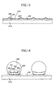
- Figures 11 - 14 are diagrams showing the fabrication process of a semiconductor device according to a second embodiment of the present invention, wherein those parts corresponding to the parts described previously are designated by the same reference numerals and the description thereof will be omitted.
- a dry etching process is conducted at the surface of the pad electrode 220 so as to include the probe flaw 240, an the probe flaw 240 is planarized.
- the Ti layer 260 and the Cu layer 61 are formed on the structure of Figure 12 consecutively by a sputtering process so as to cover the substrate protective film 230 and the pad electrode with respective thicknesses of 300nm and 200nm.
- Embodiment 1 explained wit reference to Figures 6 - 9 is conducted, and the Ni layer 280 is formed on the Cu layer 261 on the pad electrode 220 with the thickness of 4000nm and the Au layer 290 with the thickness of 200nm. Further, a lead-free solder alloy of Sn-Ag system or a lead solder alloy of Sn-Pb system is formed, and the bump electrode 300 is formed by conducting an annealing process.
- the present embodiment enables continuous and uniform formation of the Ti layer 260 and the Cu layer 261 on the pad electrode 220 continuously by planarizing the irregularity step of the probe flaw 240, and it becomes possible to form the bump electrode 300 without forming void.
- the planarization of the probe flaw 240 has been conducted by dry etching.
- Figures 15 - 16 are diagrams showing the manufacturing process of the semiconductor device according to a third embodiment of the present invention, wherein those parts in the drawing corresponding to those parts described previously are designated by the same reference numerals and the description thereof will be omitted.
- the present embodiment forms, after the probe test step, the Ti layer 262 and the Cu layer 263 by a sputtering process so as to cover the pad electrode 220 carrying thereon the probe flaw 240 and the passivation film 230, consecutively with a larger thickness of 500nm, for example.
- the Ni layer 280 is formed on the Cu layer 263 on the pad electrode 220 with the thickness of 4000nm and the Au layer with the thickness of 200nm by an electrolytic plating process as shown in Figure 16. Further, a lead-free solder alloy of the Sn-Ag system or the Pb alloy of the Sn-Pb system is formed. Further, by applying an annealing process to the solder alloy, the bump electrode 300 is formed.
- the step height of the probe flaw 240 is relatively reduced or becomes ignorable, by forming the Ti layer 262 and the Cu layer 263 with a large thickness preferably equal to or larger than the step height of the probe flaw 240, such as the thickness of about 1 ⁇ m. With this, it becomes possible to form the Ti layer 262 and the Cu layer 263 continuously on the pad electrode 220.
- the adhesion layer 260 is not limited to a Ti layer but may be formed of any of Ti, Cr, TiW, Mo, Ta, W, Nb and V.
- the electrode layer 261 is not limited to Cu but can be formed of any of Ni, Cu, Pd, Pt, Au and Ag. Further, the process of forming these is not limited to a sputtering process but evaporation deposition process or MOCVD process can also be used.
- the conductive layer 280 forming the foundation layer of the bump is not limited to the Ni layer but may be formed of an alloy containing Ni and Cu.
- the oxidation prevention layer 290 is not limited to Au but can be formed of any of Au, Pt, Pd and In.
- the bump electrode 300 is not limited to the Sn-Au alloy or Pb-Sn alloy but an alloy of Pd, Ni, Cu, Sn and Pb, or Au or Ag may also be employed.
- the present invention it becomes possible to form a conductive film on a pad electrode stably and continuously even when the pad electrode formed on a substrate carried thereon an irregular flaw.
- a conductive film on the front surface of the pad electrode.
- a bump electrode on such a conductive layer stably, without forming a void.
- the present invention it becomes possible to form a bump electrode also on the pad electrode to which the probe electrode is contacted. Thereby, the need of forming a separate pad electrode for testing is eliminated, and the substrate surface area can be used efficiently. Further, the semiconductor device can be miniaturized.
Landscapes
- Internal Circuitry In Semiconductor Integrated Circuit Devices (AREA)
- Testing Or Measuring Of Semiconductors Or The Like (AREA)
- Electrodes Of Semiconductors (AREA)
- Wire Bonding (AREA)
Abstract
Description
said pad electrode having an irregular flaw,
wherein there is provided a pattern covering said irregular flaw between said pad electrode and said bump electrode.
Claims (15)
- A semiconductor device comprising a substrate, a pad electrode formed on said substrate, and a bump electrode formed on said pad electrode, characterized in that:said pad electrode carries an irregular flaw; andthere is provided a pattern between said pad electrode and said bump electrode so as to cover said irregular flaw.
- The semiconductor device as claimed in claim 1, characterized in that said pattern comprises an inorganic film.
- The semiconductor device as claimed in claim 1, characterized in that said pattern comprises an organic film.
- The semiconductor device as claimed in claim 1, characterized in that said pattern comprises a conductive film.
- The semiconductor device as claimed in claim 1, wherein said pattern comprises a laminated film combining an inorganic film or an organic film or a conductive film.
- A manufacturing method of a semiconductor device, characterized by the steps of:forming a pad electrode on a substrate:;conducting a test by contacting a probe needle to said pad electrode;forming a pattern on a part of surface of said pad electrode so as to cover an irregularity formed by contact of said probe needle;forming a conductive film on said surface of said pad electrode so as to cover said pattern;forming a conductive foundation film on said pad electrode by an electrolytic plating process while using said conductive film as an electrode; andforming a bump electrode on said conductive foundation film.
- The manufacturing method of a semiconductor device as claimed in claim 6, characterized in that said pattern is formed of an inorganic film of a silicon nitride film or a silicon oxide film.
- The manufacturing method of a semiconductor device as claimed in claim 6, characterized in that said pattern is formed of an inorganic film of a polyimide film.
- The manufacturing method of a semiconductor device as claimed in claim 6, characterized in that said pattern comprises a conductive film of Ag, Pt, Pd and Cu of a paste state.
- A manufacturing method of a semiconductor device, characterized by the steps of:forming a pad electrode on a substrate;conducting a test by contacting a probe needle to said pad electrode;planarizing irregularity formed by contact of said probe needle;forming a conductive film on a surface of said pad electrode so as to cover said planarized irregularity;forming a conductive foundation film on said pad electrode by an electrolytic plating process while using said conductive film as an electrode; andforming a bump electrode on said conductive foundation film.
- The manufacturing method of a semiconductor device as claimed in claim 10 characterized in that said planarizing step comprises the step of dry etching said irregular flaw.
- The manufacturing method of a semiconductor device as claimed in claim 10, characterized in that said planarizing step comprises the step of wet etching said irregular flaw.
- The manufacturing method of a semiconductor device as claimed in claim 10, characterized in that said planarizing step comprises the step of fusing said pad electrode at 600 - 800°C.
- The manufacturing method of a semiconductor device characterized in that said polarizing step comprises the step of applying a pressure mechanically to said irregular flaw.
- A manufacturing method of a semiconductor device, characterized by the steps of:wherein said electrode film has a thickness exceeding a step height caused by said irregularity.forming a pad electrode on a substrate;conducting a test by contacting a probe needle to said pad electrode;forming an electrode film on a front surface of said pad electrode so as to cover an irregularity formed by contact of said probe needle;forming a conductive foundation film on said pad electrode by an electrolytic plating process while using said electrode film as an electrode; andforming a bump electrode an said conductive foundation film,
Applications Claiming Priority (1)
| Application Number | Priority Date | Filing Date | Title |
|---|---|---|---|
| PCT/JP2002/006245 WO2004001839A1 (en) | 2002-06-21 | 2002-06-21 | Semiconductor device and its producing method |
Publications (3)
| Publication Number | Publication Date |
|---|---|
| EP1517364A1 true EP1517364A1 (en) | 2005-03-23 |
| EP1517364A4 EP1517364A4 (en) | 2006-06-07 |
| EP1517364B1 EP1517364B1 (en) | 2011-03-16 |
Family
ID=29727367
Family Applications (1)
| Application Number | Title | Priority Date | Filing Date |
|---|---|---|---|
| EP02738780A Expired - Lifetime EP1517364B1 (en) | 2002-06-21 | 2002-06-21 | Semiconductor device and its producing method |
Country Status (8)
| Country | Link |
|---|---|
| US (1) | US7095045B2 (en) |
| EP (1) | EP1517364B1 (en) |
| JP (1) | JP3978449B2 (en) |
| KR (1) | KR100643645B1 (en) |
| CN (2) | CN100382262C (en) |
| DE (1) | DE60239493D1 (en) |
| TW (1) | TW546841B (en) |
| WO (1) | WO2004001839A1 (en) |
Families Citing this family (20)
| Publication number | Priority date | Publication date | Assignee | Title |
|---|---|---|---|---|
| JP4213672B2 (en) * | 2003-04-15 | 2009-01-21 | 富士通マイクロエレクトロニクス株式会社 | Semiconductor device and manufacturing method thereof |
| TWI263856B (en) | 2004-11-22 | 2006-10-11 | Au Optronics Corp | IC chip, IC assembly and flat display |
| DE102005051857A1 (en) * | 2005-05-25 | 2007-02-22 | Fraunhofer-Gesellschaft zur Förderung der angewandten Forschung e.V. | UBM-PAD, solder contact and method of making a solder joint |
| JP4998270B2 (en) | 2005-12-27 | 2012-08-15 | 富士通セミコンダクター株式会社 | Semiconductor device and manufacturing method thereof |
| KR100859641B1 (en) * | 2006-02-20 | 2008-09-23 | 주식회사 네패스 | Semiconductor with solder bump with suppressing growth of inter-metallic compound and fabrication method thereof |
| JP5050384B2 (en) | 2006-03-31 | 2012-10-17 | 富士通セミコンダクター株式会社 | Semiconductor device and manufacturing method thereof |
| JP5238206B2 (en) * | 2006-09-26 | 2013-07-17 | 株式会社フジクラ | Wiring board, electronic component and manufacturing method thereof |
| KR100857365B1 (en) * | 2007-02-28 | 2008-09-05 | 주식회사 네패스 | Bump structure of semiconductor device |
| CN101431037B (en) * | 2007-11-06 | 2011-03-30 | 宏茂微电子(上海)有限公司 | Manufacturing method of wafer level packaging structure |
| JP5627835B2 (en) * | 2007-11-16 | 2014-11-19 | ローム株式会社 | Semiconductor device and manufacturing method of semiconductor device |
| TWI394253B (en) * | 2009-03-25 | 2013-04-21 | 日月光半導體製造股份有限公司 | Package structure of bumped wafer and bumped wafer |
| JP2011165862A (en) * | 2010-02-09 | 2011-08-25 | Sony Corp | Semiconductor device, chip-on-chip mounting structure, method for manufacturing semiconductor device, and method for forming chip-on-chip mounting structure |
| US8492892B2 (en) * | 2010-12-08 | 2013-07-23 | International Business Machines Corporation | Solder bump connections |
| US9941176B2 (en) * | 2012-05-21 | 2018-04-10 | Taiwan Semiconductor Manufacturing Company, Ltd. | Selective solder bump formation on wafer |
| US9537066B2 (en) * | 2013-07-30 | 2017-01-03 | Dowa Electronics Materials Co., Ltd. | Method of manufacturing semiconductor light emitting device, and semiconductor light emitting device |
| US8779604B1 (en) * | 2013-11-06 | 2014-07-15 | Chipmos Technologies Inc. | Semiconductor structure and manufacturing method thereof |
| JP6450560B2 (en) * | 2014-10-24 | 2019-01-09 | 新日本無線株式会社 | Semiconductor device and manufacturing method thereof |
| CN108962431B (en) * | 2017-05-23 | 2024-07-02 | 上海昊佰智造精密电子股份有限公司 | Single-layer conductive cloth and die cutting device for same |
| CN112366131B (en) | 2020-10-21 | 2023-01-03 | 武汉新芯集成电路制造有限公司 | Method for manufacturing semiconductor device |
| CN115708203B (en) * | 2021-08-19 | 2025-08-01 | 长鑫存储技术有限公司 | Semiconductor structure and preparation method thereof |
Family Cites Families (13)
| Publication number | Priority date | Publication date | Assignee | Title |
|---|---|---|---|---|
| JPS61253847A (en) * | 1985-05-02 | 1986-11-11 | Nec Corp | Highly reliable semiconductor device |
| JPS63249346A (en) * | 1987-04-03 | 1988-10-17 | Fujitsu Ltd | Pad in integrated circuit chip and formation thereof |
| JPH01295444A (en) * | 1988-02-09 | 1989-11-29 | Fujitsu Ltd | Manufacture of semiconductor device |
| JPH06267884A (en) * | 1993-03-12 | 1994-09-22 | Mitsubishi Electric Corp | Method for manufacturing semiconductor device |
| KR100327442B1 (en) * | 1995-07-14 | 2002-06-29 | 구본준, 론 위라하디락사 | Bump Structure and Forming Method of Semiconductor Device |
| JP3756234B2 (en) * | 1996-02-22 | 2006-03-15 | ローム株式会社 | Semiconductor device including semiconductor chip and functional test trace repair method for the chip |
| JP3504421B2 (en) * | 1996-03-12 | 2004-03-08 | 株式会社ルネサステクノロジ | Semiconductor device |
| JP3335562B2 (en) * | 1997-08-20 | 2002-10-21 | 富士通株式会社 | Semiconductor chip connection bump forming method |
| JP3638085B2 (en) * | 1998-08-17 | 2005-04-13 | 富士通株式会社 | Semiconductor device |
| US6251694B1 (en) * | 1999-05-26 | 2001-06-26 | United Microelectronics Corp. | Method of testing and packaging a semiconductor chip |
| TW466655B (en) * | 2001-02-23 | 2001-12-01 | Megic Corp | Flip chip and the manufacturing process thereof |
| US6782895B2 (en) * | 2001-08-20 | 2004-08-31 | L'oreal, S.A. | Compositions comprising at least one hydroxide compound and at least one complexing agent, and methods for using the same |
| US6782897B2 (en) * | 2002-05-23 | 2004-08-31 | Taiwan Semiconductor Manufacturing Co., Ltd. | Method of protecting a passivation layer during solder bump formation |
-
2002
- 2002-06-21 CN CNB028291050A patent/CN100382262C/en not_active Expired - Fee Related
- 2002-06-21 JP JP2004515450A patent/JP3978449B2/en not_active Expired - Fee Related
- 2002-06-21 KR KR1020047019063A patent/KR100643645B1/en not_active Expired - Fee Related
- 2002-06-21 EP EP02738780A patent/EP1517364B1/en not_active Expired - Lifetime
- 2002-06-21 WO PCT/JP2002/006245 patent/WO2004001839A1/en not_active Ceased
- 2002-06-21 DE DE60239493T patent/DE60239493D1/en not_active Expired - Lifetime
- 2002-06-21 CN CNB2007101807338A patent/CN100536103C/en not_active Expired - Fee Related
- 2002-06-27 TW TW091114197A patent/TW546841B/en not_active IP Right Cessation
-
2004
- 2004-11-29 US US10/998,182 patent/US7095045B2/en not_active Expired - Fee Related
Also Published As
| Publication number | Publication date |
|---|---|
| TW546841B (en) | 2003-08-11 |
| JPWO2004001839A1 (en) | 2005-10-27 |
| JP3978449B2 (en) | 2007-09-19 |
| KR20040111695A (en) | 2004-12-31 |
| KR100643645B1 (en) | 2006-11-10 |
| CN101145533A (en) | 2008-03-19 |
| EP1517364B1 (en) | 2011-03-16 |
| DE60239493D1 (en) | 2011-04-28 |
| CN100536103C (en) | 2009-09-02 |
| WO2004001839A1 (en) | 2003-12-31 |
| CN100382262C (en) | 2008-04-16 |
| CN1628379A (en) | 2005-06-15 |
| US7095045B2 (en) | 2006-08-22 |
| US20050151250A1 (en) | 2005-07-14 |
| EP1517364A4 (en) | 2006-06-07 |
Similar Documents
| Publication | Publication Date | Title |
|---|---|---|
| EP1517364B1 (en) | Semiconductor device and its producing method | |
| US6756688B2 (en) | Wiring board and its production method, semiconductor device and its production method, and electronic apparatus | |
| US8901733B2 (en) | Reliable metal bumps on top of I/O pads after removal of test probe marks | |
| EP1842233B1 (en) | Method of forming bump sites on bond-pads | |
| US5492235A (en) | Process for single mask C4 solder bump fabrication | |
| US5418186A (en) | Method for manufacturing a bump on a semiconductor chip | |
| US8507317B2 (en) | Solder bump structure for flip chip semiconductor devices and method of manufacturing therefore | |
| US8723322B2 (en) | Method of metal sputtering for integrated circuit metal routing | |
| US6613663B2 (en) | Method for forming barrier layers for solder bumps | |
| US20080023836A1 (en) | Semiconductor device | |
| US20020093098A1 (en) | Semiconductor device and method of formation | |
| US7508082B2 (en) | Semiconductor device and method of manufacturing the same | |
| JP2000183090A (en) | Chip size package and manufacturing method thereof | |
| US6706622B1 (en) | Bonding pad interface | |
| US20040048458A1 (en) | Fabrication method for strengthening flip-chip solder bumps | |
| JP4702827B2 (en) | Semiconductor device and manufacturing method thereof | |
| CN1103119C (en) | Method for Single Mask C4 Solder Bump Fabrication | |
| JPH0494135A (en) | Field effect transistor | |
| JP2000228486A (en) | Semiconductor chip and semiconductor device with chip-on-chip structure | |
| JPH0831831A (en) | Semiconductor integrated circuit device and manufacturing method thereof |
Legal Events
| Date | Code | Title | Description |
|---|---|---|---|
| PUAI | Public reference made under article 153(3) epc to a published international application that has entered the european phase |
Free format text: ORIGINAL CODE: 0009012 |
|
| 17P | Request for examination filed |
Effective date: 20041122 |
|
| AK | Designated contracting states |
Kind code of ref document: A1 Designated state(s): AT BE CH CY DE DK ES FI FR GB GR IE IT LI LU MC NL PT SE TR |
|
| AX | Request for extension of the european patent |
Extension state: AL LT LV MK RO SI |
|
| DAX | Request for extension of the european patent (deleted) | ||
| RBV | Designated contracting states (corrected) |
Designated state(s): DE FR GB |
|
| A4 | Supplementary search report drawn up and despatched |
Effective date: 20060425 |
|
| 17Q | First examination report despatched |
Effective date: 20080411 |
|
| RAP1 | Party data changed (applicant data changed or rights of an application transferred) |
Owner name: FUJITSU MICROELECTRONICS LIMITED |
|
| RAP1 | Party data changed (applicant data changed or rights of an application transferred) |
Owner name: FUJITSU SEMICONDUCTOR LIMITED |
|
| GRAP | Despatch of communication of intention to grant a patent |
Free format text: ORIGINAL CODE: EPIDOSNIGR1 |
|
| GRAS | Grant fee paid |
Free format text: ORIGINAL CODE: EPIDOSNIGR3 |
|
| RIN1 | Information on inventor provided before grant (corrected) |
Inventor name: MISAWA, KAZUHIRO,C/O FUJITSU INTEGRATED MICROTECHN Inventor name: SATOH, AKIRA,C/O FUJITSU INTEGRATED MICROTECHNOLOG Inventor name: TAMAGAWA, MICHIAKI,C/O FUJITSU INTEGRATED MICROTEC Inventor name: WATANABE, EIJI,C/O FUJITSU LIMITED Inventor name: MURATA, KOICHI,C/O FUJITSU LIMITED Inventor name: ISHIGURI, MASAHIKO,C/O FUJITSU LIMITED Inventor name: CHIBA, SHUICHI,C/O FUJITSU LIMITED Inventor name: TOIDA, YASUSHI,C/O FUJITSU INTEGRATED MICROTECHNOL |
|
| GRAA | (expected) grant |
Free format text: ORIGINAL CODE: 0009210 |
|
| AK | Designated contracting states |
Kind code of ref document: B1 Designated state(s): DE FR GB |
|
| REG | Reference to a national code |
Ref country code: GB Ref legal event code: FG4D |
|
| REF | Corresponds to: |
Ref document number: 60239493 Country of ref document: DE Date of ref document: 20110428 Kind code of ref document: P |
|
| REG | Reference to a national code |
Ref country code: DE Ref legal event code: R096 Ref document number: 60239493 Country of ref document: DE Effective date: 20110428 |
|
| PLBE | No opposition filed within time limit |
Free format text: ORIGINAL CODE: 0009261 |
|
| STAA | Information on the status of an ep patent application or granted ep patent |
Free format text: STATUS: NO OPPOSITION FILED WITHIN TIME LIMIT |
|
| 26N | No opposition filed |
Effective date: 20111219 |
|
| GBPC | Gb: european patent ceased through non-payment of renewal fee |
Effective date: 20110621 |
|
| REG | Reference to a national code |
Ref country code: FR Ref legal event code: ST Effective date: 20120229 |
|
| REG | Reference to a national code |
Ref country code: DE Ref legal event code: R097 Ref document number: 60239493 Country of ref document: DE Effective date: 20111219 |
|
| PG25 | Lapsed in a contracting state [announced via postgrant information from national office to epo] |
Ref country code: FR Free format text: LAPSE BECAUSE OF NON-PAYMENT OF DUE FEES Effective date: 20110630 |
|
| PG25 | Lapsed in a contracting state [announced via postgrant information from national office to epo] |
Ref country code: GB Free format text: LAPSE BECAUSE OF NON-PAYMENT OF DUE FEES Effective date: 20110621 |
|
| REG | Reference to a national code |
Ref country code: DE Ref legal event code: R082 Ref document number: 60239493 Country of ref document: DE Representative=s name: REICHERT & LINDNER PARTNERSCHAFT PATENTANWAELT, DE |
|
| REG | Reference to a national code |
Ref country code: DE Ref legal event code: R082 Ref document number: 60239493 Country of ref document: DE Representative=s name: REICHERT & LINDNER PARTNERSCHAFT PATENTANWAELT, DE Effective date: 20150512 Ref country code: DE Ref legal event code: R081 Ref document number: 60239493 Country of ref document: DE Owner name: SOCIONEXT INC., YOKOHAMA-SHI, JP Free format text: FORMER OWNER: FUJITSU SEMICONDUCTOR LTD., YOKOHAMA, KANAGAWA, JP Effective date: 20150512 |
|
| PGFP | Annual fee paid to national office [announced via postgrant information from national office to epo] |
Ref country code: DE Payment date: 20170613 Year of fee payment: 16 |
|
| REG | Reference to a national code |
Ref country code: DE Ref legal event code: R119 Ref document number: 60239493 Country of ref document: DE |
|
| PG25 | Lapsed in a contracting state [announced via postgrant information from national office to epo] |
Ref country code: DE Free format text: LAPSE BECAUSE OF NON-PAYMENT OF DUE FEES Effective date: 20190101 |