EP1517356A2 - Electron-beam lithography method and device - Google Patents
Electron-beam lithography method and device Download PDFInfo
- Publication number
- EP1517356A2 EP1517356A2 EP04255329A EP04255329A EP1517356A2 EP 1517356 A2 EP1517356 A2 EP 1517356A2 EP 04255329 A EP04255329 A EP 04255329A EP 04255329 A EP04255329 A EP 04255329A EP 1517356 A2 EP1517356 A2 EP 1517356A2
- Authority
- EP
- European Patent Office
- Prior art keywords
- electron
- electron beam
- angular position
- reference angular
- substrate
- Prior art date
- Legal status (The legal status is an assumption and is not a legal conclusion. Google has not performed a legal analysis and makes no representation as to the accuracy of the status listed.)
- Granted
Links
Images




Classifications
-
- G—PHYSICS
- G02—OPTICS
- G02B—OPTICAL ELEMENTS, SYSTEMS OR APPARATUS
- G02B5/00—Optical elements other than lenses
- G02B5/18—Diffraction gratings
- G02B5/1847—Manufacturing methods
- G02B5/1857—Manufacturing methods using exposure or etching means, e.g. holography, photolithography, exposure to electron or ion beams
-
- B—PERFORMING OPERATIONS; TRANSPORTING
- B82—NANOTECHNOLOGY
- B82Y—SPECIFIC USES OR APPLICATIONS OF NANOSTRUCTURES; MEASUREMENT OR ANALYSIS OF NANOSTRUCTURES; MANUFACTURE OR TREATMENT OF NANOSTRUCTURES
- B82Y10/00—Nanotechnology for information processing, storage or transmission, e.g. quantum computing or single electron logic
-
- B—PERFORMING OPERATIONS; TRANSPORTING
- B82—NANOTECHNOLOGY
- B82Y—SPECIFIC USES OR APPLICATIONS OF NANOSTRUCTURES; MEASUREMENT OR ANALYSIS OF NANOSTRUCTURES; MANUFACTURE OR TREATMENT OF NANOSTRUCTURES
- B82Y40/00—Manufacture or treatment of nanostructures
-
- H—ELECTRICITY
- H01—ELECTRIC ELEMENTS
- H01J—ELECTRIC DISCHARGE TUBES OR DISCHARGE LAMPS
- H01J37/00—Discharge tubes with provision for introducing objects or material to be exposed to the discharge, e.g. for the purpose of examination or processing thereof
- H01J37/30—Electron-beam or ion-beam tubes for localised treatment of objects
- H01J37/317—Electron-beam or ion-beam tubes for localised treatment of objects for changing properties of the objects or for applying thin layers thereon, e.g. for ion implantation
- H01J37/3174—Particle-beam lithography, e.g. electron beam lithography
-
- H—ELECTRICITY
- H01—ELECTRIC ELEMENTS
- H01J—ELECTRIC DISCHARGE TUBES OR DISCHARGE LAMPS
- H01J2237/00—Discharge tubes exposing object to beam, e.g. for analysis treatment, etching, imaging
- H01J2237/20—Positioning, supporting, modifying or maintaining the physical state of objects being observed or treated
- H01J2237/202—Movement
- H01J2237/20214—Rotation
-
- H—ELECTRICITY
- H01—ELECTRIC ELEMENTS
- H01J—ELECTRIC DISCHARGE TUBES OR DISCHARGE LAMPS
- H01J2237/00—Discharge tubes exposing object to beam, e.g. for analysis treatment, etching, imaging
- H01J2237/20—Positioning, supporting, modifying or maintaining the physical state of objects being observed or treated
- H01J2237/202—Movement
- H01J2237/20278—Motorised movement
-
- H—ELECTRICITY
- H01—ELECTRIC ELEMENTS
- H01J—ELECTRIC DISCHARGE TUBES OR DISCHARGE LAMPS
- H01J2237/00—Discharge tubes exposing object to beam, e.g. for analysis treatment, etching, imaging
- H01J2237/30—Electron or ion beam tubes for processing objects
- H01J2237/317—Processing objects on a microscale
- H01J2237/3175—Lithography
- H01J2237/31761—Patterning strategy
- H01J2237/31766—Continuous moving of wafer
Definitions
- the present invention relates to a method and device of electron-beam lithography suitable for fabricating a diffraction grating, a Fresnel lens, a photonic crystal, or other optical elements with an electron beam.
- a diffraction grating, a Fresnel lens, and the like are fabricated in the following way. First, expose a resist by interference lithography to form a pattern, etch a substrate with the resist as a mask, form an inverted mold with the substrate as a mask, and then transfer the shape of the inverted mold to a resin or the like to form the desired optical element.
- an electron-beam lithography apparatus is frequently used to irradiate a resist applied on a substrate with an electron beam to form a pattern, as disclosed in Japanese Laid-Open Patent Application No. 7-294730 (below, referred to as reference 1), and in Japanese Patent Gazette No. 2853659 (below, referred to as reference 2).
- electron-beam lithography is also used when fabricating a photonic crystal.
- an optical element Differing from a semiconductor element, an optical element usually has a relatively large area, for example, in a range from several mm 2 to several cm 2 , and hence, relative positional accuracy inside the area is important when fabricating the optical element.
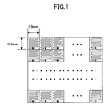
- FIG. 1 is view showing an example of the electron-beam lithography method in the related art.
- an electron beam is deflected in x or y directions to expose a predetermined portion of a surface of a substrate.
- This predetermined portion is referred to as a "unit exposure field", defined to be a region able to be exposed by only deflecting the electron beam without moving a sample stage (or called xy stage) that supports the substrate.
- xy stage sample stage
- y-stage lithography apparatus this electron-beam lithography apparatus is referred to as "xy-stage lithography apparatus”.
- the electron beam is deflected to scan the unit exposure field. If the electron beam is deflected too much, at ends of the unit exposure field, the electron beam becomes de-focused. For this reason, the area of the unit exposure field has to be limited to be small, for example, in the xy-stage lithography apparatus, the unit exposure field is at most 2 mm x 2 mm in area, and usually, only about 0.5 mm x 0.5 mm.
- the highest position alignment precision of the xy-stage lithography apparatus is around 0.05 ⁇ m, and hence, at least uncertainty in position alignment at this level exists between unit exposure fields.
- the xy-stage is moved in the x or y directions.
- Other methods of moving a sample stage are also proposed.
- a disk lithography apparatus a disk material of an optical disk is placed on a turning table, and an electron beam is incident on the disk material while the disk material is rotating to form a pattern on the disk material.
- this kind of lithography apparatus is referred to as an "x ⁇ -stage lithography apparatus”.
- FIG. 2 is a schematic view of an exemplary configuration of the disk lithography apparatus.
- the disk lithography apparatus includes a cylinder 1 and a sample chamber 2.
- a cylinder 1 there are arranged an electron gun 4, an electromagnetic lens 6, blanking electrodes 9, a diaphragm 10, a deflector 11, and an electromagnetic lens 8.
- the sample chamber 2 there are arranged a turning table 14 on which a disk material 13 is arranged, a spindle motor 17 that drives the turning table 14 to rotate, and a translational stage 15 that movably (in a sliding direction) supports the spindle motor 17.
- An electron beam 5 is generated in the electron gun 4 and directed onto the disk material 13 by the electromagnetic lens 6, blanking electrodes 9, deflector 11, and the electromagnetic lens 8.
- the disk lithography apparatus in FIG. 2 further includes a detector 3 that measures the position of the translational stage 15, a motor 16 that drives the translational stage 15, a transverse driver 21 that controls and drives the motor 16, a spindle driver 22 that controls and drives the spindle motor 17, a blanking driver 23 that controls and drives the blanking electrodes 9, a deflector driver 24 that controls and drives the deflector 11, a pulse generator 25 that outputs pulses to the transverse driver 21 and the spindle driver 22 based on the measurement results of the detector 3, and a formatter 26 that outputs control signals to the blanking driver 23 and the deflector driver 24.
- a detector 3 that measures the position of the translational stage 15, a motor 16 that drives the translational stage 15, a transverse driver 21 that controls and drives the motor 16, a spindle driver 22 that controls and drives the spindle motor 17, a blanking driver 23 that controls and drives the blanking electrodes 9, a deflector driver 24 that controls and drives the deflector 11, a pulse generator 25 that outputs
- the cylinder 1 is evacuated to a vacuum higher than 10 -5 torr.
- the electron beam 5 generated in the electron gun 4 in the cylinder 1 is focused by the electromagnetic lens 6, and the size of the electron beam 5 is limited by the diaphragm 10.
- the electron beam 5 is deflected intermittently by the blanking electrodes 9 according to a signal from the formatter 26 to switch the electron beam 5 ON or OFF.
- the electron beam 5 is then focused by the electromagnetic lens 8, and is directed to irradiate the disk material 13.
- the disk material 13 is rotated, together with the turning table 14, at a preset linear velocity, while being moved along a radial direction at preset pitches by the translational stage 15. As a result, the electron beam 5 forms a spiral track on the disk material 13.
- the electron beam 5 may also be deflected periodically by the deflector 11.
- precise position alignment is achievable by measuring the position of the translational stage 15 with the detector 3 when the translational stage 15 is moving.
- the unit exposure field, in which precise position alignment is achievable, is small, and it is not sufficient for forming an optical element.
- the xy stage can be moved in x, y directions repeatedly to expose many unit exposure fields to form a pattern, in this case, position misalignment occurs between unit exposure fields.
- Japanese Laid-Open Patent Application No. 2000-207738 (below, referred to as reference 4) discloses an invention related to this technique.
- exposure can be carried out while modulating the flux of the laser beam along the radial directions, for example, by performing CAV (Constant Angular Velocity) control, to compensate for variation in the laser beam flux for exposure, which is attributed to the dependence of linear velocity on the radius.
- CAV Constant Angular Velocity
- a specific object of the present invention is to provide an electron-beam lithography method and device capable of forming a pattern of any kind of shape with high precision in a large area.
- an electron-beam lithography method for irradiating a rotating substrate with an electron beam while moving an irradiation position of the electron beam on the substrate in a radial direction at predetermined pitches.
- the electron-beam lithography method includes the steps of setting a portion of a region able to be irradiated by the electron beam to be a pattern exposure region; controlling the rotational speed of the substrate to be V/2 ⁇ r at a radial position r at a reference angular position when the irradiation position of the electron beam is in the pattern exposure region, where V represents the linear velocity at the reference angular position; changing the rotational speed to a value corresponding to a next radial position when the irradiation position of the electron beam is out of the pattern exposure region, and controlling the electron beam intermittently according to time after changing the rotational speed relative to the reference angular position.
- the rotational speed is changed at a predetermined angular position out of the pattern exposure region.
- the irradiation position is changed at a predetermined angular position out of the pattern exposure region.
- the irradiation position is changed by a distance equaling zero or integral multiples of the pitch.
- the electron beam is deflected in a direction parallel to a direction at the reference angular position so that tracks of the electron beam in the pattern exposure region are perpendicular to the direction at the reference angular position.
- the electron beam is deflected in a direction perpendicular to a direction at the reference angular position so that a distance from the reference angular position to a position of the electron beam after predetermined time elapses is constant at different radii.
- a plurality of the reference angular positions are arranged; and a plurality of the pattern exposure regions are arranged.
- an electron-beam lithography apparatus that generates an electron beam to irradiate a surface of a rotating substrate to form a pattern.
- the electron-beam lithography apparatus includes a rotation stage that rotates the substrate; a translatory stage that moves the substrate along a radial direction; a detection unit that detects a reference angular position of the translatory stage; a rotation controller that detects a radial position of an irradiation position of the electron beam at reference angular position, and changes a rotational speed of the substrate based on the detected radial position; a deflection unit that deflects the electron beam in the radial direction and in a rotation direction; and an exposure unit that exposes a pattern exposure region with the electron beam in a tangential direction of the rotation stage according to time elapsed relative to the reference angular position, said pattern exposure region being a portion of a region able to be irradiated by the electron beam.
- an x ⁇ -stage electron-beam lithography apparatus by controlling exposure by the electron beam according to time information relative to the reference angular position, it is possible to expose a large area without the problem in position alignment between adjacent exposure fields occurring in an xy-stage electron-beam lithography apparatus of the related art.
- any position inside in the pattern exposure region can be expressed accurately from time information obtained from the radius and the reference angular position, and it is possible to perform exposure in a large area with high precision.
- FIG. 3 is a schematic view showing an exemplary configuration of an electron-beam lithography apparatus according to a first embodiment of the present invention.
- the same reference numbers are used for the same elements as those shown in FIG. 2, and overlapping descriptions are omitted.
- the reference number 30 designates a substrate on which a resist is applied.
- FIG. 4 is schematic view showing the process of forming a pattern by irradiating the substrate 30 with an electron beam while rotating the substrate 30 together with the turning table 14.
- the reference number 12 designates a reference angular position
- the reference number 18 designates an exposure region.
- the exposure region 18 is a rectangle, and one side of the exposure region 18 is set at the reference angular position 12.
- the electron beam 5 forms spiral tracks 7 on the substrate 30. Inside the exposure region 18, the tracks 7 of the electron beam 5 appear as arcs, and are distributed at equal intervals.
- the linear velocity changes along the radial directions, hence, the exposure dose of the electron beam along the radial directions cannot be constant. It may be attempted to modulate the intensity of the electron beam along the radial directions, for example, by making the intensity of the electron beam variable, but, as mentioned above, it is difficult.
- a rotary encoder for example, in FIG. 2, if the diameter of the turning table 14 is 150 mm, and the exposure region is 10 mm x 20 mm, even when 100 million pulses are assigned to one revolution, at a radial position of 60 mm on the turning table, one pulse corresponds to a distance as long as 11 ⁇ m. Thus, it is impossible to obtain accuracy of the exposure position as high as that obtained in the lithography apparatus of the related art.
- the method of electron-beam lithography according to the first embodiment of the present invention is proposed to solve this problem.
- FIG. 5 is a schematic view of a pattern n exposed by the electron-beam lithography method of the present embodiment.
- the reference number 35 designates a selected angular position.
- the selected angular position 35 is set to be out of the exposure region 18.
- the y axis is set to be the reference angular position 12
- the x axis that is, the angular position after the turning table 14 rotates 90 degrees from the reference angular position 12 is set to be the selected angular position 35.
- the method of electron-beam lithography according to the first embodiment of the present invention is executed by using the electron-beam lithography apparatus shown in FIG. 3.
- the rotational speed of the turning table 14 is represented by k (rps)
- a radial position (that is, a radius) at the reference angular position 12 is represented by r (mm)
- a linear velocity at the reference angular position 12 is represented by V (mm/s).
- the rotational speed k is controlled to be V/2 ⁇ r at each radius r.
- the reference angular position 12 is detected from the pulse related to the original point of the turning table 14, and a pulse from a rotary encoder.
- the radial position is changed at the selected angular position 35, which is at a specified position apart from the reference angular position 12, while taking into consideration the time required by radial position control.
- the rotational speed is changed at the same time as the radial position is changed.
- the radial position changes by one pitch after one revolution.
- the radial position may change by one pitch after a plurality of revolutions, or the radial position may change by multiple pitches after one revolution. Therefore, preferably, movement of the translational stage 15 is controlled so that the change of the radial position is zero or integral multiples of the pitch.
- the exposure position of the electron beam 5 can be accurately expressed by using the time from the reference angular position 12 as a parameter.
- the starting position for counting the time is at the reference angular position 12, as illustrated in FIG. 5, this starting position may be at any other appropriate angular position.
- coordinates (x, y) of an exposure position of the electron beam 5 after time t (seconds) elapses from the reference angular position 12 can be expressed by the following equation (1).
- (x, y) (r*sin(2 ⁇ kt), r*cos(2 ⁇ kt)) where, r represents a radius in units of mm.
- FIG. 6 is a view of a coordinate system illustrating the relation expressed by the equation (1).
- the above method is suitable for formation of a circular pattern.
- the xy-stage lithography apparatus which is expressed by x, y coordinates
- it is required to transform the x, y coordinates into x, ⁇ coordinates.
- uncertainties occur in this transformation.
- the uncertainties may be at most half of the pitch.
- the exposure pitch is reduced in order to reduce the uncertainties arising when transforming the x, y coordinates into x, ⁇ coordinates. But this method of reducing the pitch has limits.
- the methods described in the subsequent second and third embodiments are for solving this problem, in which, when irradiating the exposure region 18 using the lithography apparatus shown in FIG. 3, the electron beam 5 is deflected in x or y directions in the exposure region 18.
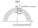
- FIG. 7 is a schematic view showing tracks of the electron beam 5 in the exposure region 18, which are formed by an electron-beam lithography method according to a second embodiment of the present invention.
- the electron beam 5 is deflected in the y direction when exposing in the exposure region 18, which is defined in the first embodiment.
- the deflector 11 is controlled so that the tracks of the electron beam 5 are perpendicular to the y axis (or parallel to the x axis), which is at the reference angular position 12.
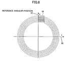
- FIG. 8 is a schematic view showing the tracks of an electron beam in the exposure region 18 and over the substrate 30, according to the present embodiment.
- the radial position and the rotational speed are changed at the selected angular position 35, which is at a specified position apart from the reference angular position 12, while taking into consideration the time required by radial position control.
- the radial position and the rotational speed can be changed at the same time.
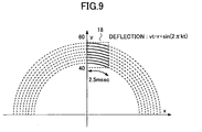
- FIG. 9 is a schematic view showing tracks of the electron beam 5 in the exposure region 18, which are formed by an electron-beam lithography method according to a third embodiment of the present invention.
- the electron beam 5 is deflected in the x direction when exposing the exposure region 18.
- the deflector 11 is controlled so that the distance between the reference angular position 12 (y axis) and the position of the electron beam after a certain time interval elapses from the reference angular position 12 is constant at different radial positions in the exposure region 18.
- the coordinates (x, y) of an exposure position of the electron beam 5 after time t (seconds) elapses from the reference angular position 12 can be simply expressed to be (Vt, r).
- data of drawings created by CAD or other applications, which are described with x, y coordinates can be transformed directly to signals of the formatter 26, and thus uncertainties do not occur when transforming the x, y coordinates into x, ⁇ coordinates.
- unit exposure fields each of which is usually 0.5 mm x 0.5 mm in area, are exposed by repeating deflection in the x direction by a distance of 0.5 mm and deflection and movement in the y direction by one pitch (in this case, the deflected distance is ⁇ 0.25mm).
- the deflection in the y direction results in reduction of the radius
- the radius is set to have a large offset in advance, for example, the offset is 0.25 mm in the above example
- the deflection ⁇ y in the y direction may be 1/2.
- the electron beam is scanned by the same deflection (0.25 mm) as that in the xy-stage lithography apparatus of the related art, by setting an offset in advance, it is possible to expose a region having an area of 7 mm x 7 mm.
- FIGs. 10A through 10C illustrate a diffraction grating formed by utilizing the methods of the second embodiment and the third embodiment, where FIG. 10A is a perspective view of the diffraction grating, FIG. 10B is a graph showing exposure dose, and FIG. 10C shows exposure pulses of different laps of a track of the electron beam.
- the diffraction grating in FIG. 10A includes a glass substrate 40 and a PMMA (polymethylmethacrylate) film 41 on the glass substrate 40.
- the exposure dose is set variable.
- the residual film of the PMMA film 41 after development is modulated, forming a diffraction grating as shown in FIG. 10A.
- the variation of the exposure dose is set in the way illustrated in FIG. 10C.
- FIG. 10C exposure is performed 10 laps by 10 laps, and the respective exposure pulses for the 10 laps are illustrated in FIG. 10C, that is, the width of the exposure pulse for the first lap is the largest, the widths of the exposure pulses for the successive laps decrease gradually, and the width of the exposure pulse for the 10th lap is the smallest.
- the initial position of the electron beam scanning in the exposure region 18 is set as the reference angular position 12.
- the reference angular position 12 may also be set at other positions.
- FIG. 11 is a schematic view showing another example of a pattern exposed by the electron-beam lithography methods of the present invention.
- the -x direction which is 90 degrees earlier than the exposure region 18, is set to be the reference angular position 12, thus, at a radius r (mm), the coordinates (x, y) of an exposure position after t (seconds) elapses from the reference angular position (-x axis) can be expressed by the following equation (6).
- (x, y) (-r*cos(2 ⁇ r/V-t)* 2 ⁇ k, -r*sin(2 ⁇ r/V-t)* 2 ⁇ k)
- the exposure region is two times the exposure region 18 in FIG. 8 and FIG. 9. Therefore, it is possible to easily form a long and thin optical element, such as an f ⁇ lens having a fine diffraction pattern on its surface.
- the translational stage 15 is driven to move at a selected angular position only when necessary, and is repeatedly moved and stopped. In the present embodiment, the translational stage 15 is driven to move continuously in the course of exposure.
- the translational stage 15 is controlled so that a radial position (radius) r (mm) after t (seconds) elapses can be expressed by the following equation (7).
- r [(t*P)/( ⁇ *V)+r0 2 ] 1/2
- P represents a pitch in units of ⁇ m
- V represents a linear velocity in units of (mm/s)
- r0 represents an initial exposure radius in units of (mm).
- the electron beam 5 is deflected in the same way as described in the second and third embodiments.
- the translational stage 15 is moved even in the course of exposure. Assume the translational stage 15 moves through a distance ⁇ r (displacement) after t (seconds) elapses from a radial position r1 (mm) at the reference angular position 12.
- the displacement ⁇ r of the translational stage 15 is less than 7 nm.
- the displacement ⁇ r of the translational stage 15 is negligible, and the same as the second and third embodiments, by deflections in the x and y directions, data of drawings created by CAD or other applications, which are described with x, y coordinates, can be transformed directly to signals of the formatter 26.
- the displacement ⁇ r can be diminished by appropriately setting the deflection ⁇ y in the y direction.
- the translational stage 15 moves more continuously, and when forming a pattern by switching the beam irradiation ON/OFF, it is possible to obtain a position feeding accuracy higher than that in the first embodiment, in which the translational stage 15 moves discontinuously; moreover, it does not take any time to determine the feeding position.
- FIG. 12 is a schematic view showing an example of providing a plurality of exposure regions.
- FIG. 13 is a view of a photonic crystal wave guide path formed by the method shown in FIG. 12.
- an electron-beam resist is applied on a Si wafer, on which a SiO 2 film is formed.
- a plurality of circular patterns each having a diameter of 0.2 ⁇ m are distributed at equal pitches of 0.6 ⁇ m, and the patterns shown in FIG. 13 are formed by RIE (Reactive Ion Etching).
- the wave guide loss of the thus formed photonic crystal wave guide path was measured at a wavelength 1400 nm, and the result was 7 dB/mm, which is sufficiently small.
- the method of lithography of the present embodiment is suitable for forming an optical element larger than several mm 2 with high precision, on which many cylindrical holes, each of which is several hundred nano-meters in diameter, are arranged at intervals of about several hundred nm such as a photonic crystal wave guide path.
Landscapes
- Engineering & Computer Science (AREA)
- Chemical & Material Sciences (AREA)
- Nanotechnology (AREA)
- Physics & Mathematics (AREA)
- General Physics & Mathematics (AREA)
- Crystallography & Structural Chemistry (AREA)
- Manufacturing & Machinery (AREA)
- Mathematical Physics (AREA)
- Theoretical Computer Science (AREA)
- Optics & Photonics (AREA)
- Condensed Matter Physics & Semiconductors (AREA)
- Analytical Chemistry (AREA)
- Electron Beam Exposure (AREA)
- Exposure And Positioning Against Photoresist Photosensitive Materials (AREA)
- Diffracting Gratings Or Hologram Optical Elements (AREA)
Abstract
Description
Claims (9)
- An electron-beam lithography method for irradiating a rotating substrate with an electron beam while moving an irradiation position of the electron beam on the substrate in a radial direction at predetermined pitches, said electron-beam lithography method comprising the steps of:setting a portion of a region able to be irradiated by the electron beam to be a pattern exposure region;controlling a rotational speed of the substrate to be V/2πr at a radial position r at a reference angular position when the irradiation position of the electron beam is in the pattern exposure region, where V represents a linear velocity at the reference angular position;changing the rotational speed to a value corresponding to a next radial position when the irradiation position of the electron beam is out of the pattern exposure region; andcontrolling the electron beam intermittently according to time after changing the rotational speed relative to the reference angular position.
- The electron-beam lithography method as claimed in claim 1, wherein
the rotational speed is changed at a predetermined angular position out of the pattern exposure region. - The electron-beam lithography method as claimed in claim 1, wherein
the irradiation position is changed at a predetermined angular position out of the pattern exposure region. - The electron-beam lithography method as claimed in claim 3, wherein
the irradiation position is changed by a distance equaling zero or integral multiples of the pitch. - The electron-beam lithography method as claimed in claim 1, wherein
a translational stage that moves the substrate in the radial directions is controlled so that a radial position r after time t elapses is expressed by r = [(t*P) / (π*V)+r02]1/2,
where, P represents a pitch, V represents a linear velocity, and r0 represents an initial exposure radius; and
the irradiation position is changed at a predetermined angular position out of the pattern exposure region. - The electron-beam lithography method as claimed in claim 1, wherein
the electron beam is deflected in a direction parallel to a direction at the reference angular position so that tracks of the electron beam in the pattern exposure region are perpendicular to the direction at the reference angular position. - The electron-beam lithography method as claimed in claim 1, wherein
the electron beam is deflected in a direction perpendicular to a direction at the reference angular position so that a distance from the reference angular position to a position of the electron beam after predetermined time elapses is constant at different radii. - The electron-beam lithography method as claimed in claim 1, wherein
a plurality of the reference angular positions are arranged; and
a plurality of the pattern exposure regions are arranged. - An electron-beam lithography apparatus that generates an electron beam to irradiate a surface of a rotating substrate to form a pattern, said electron-beam lithography apparatus comprising:a rotation stage that rotates the substrate;a translational stage that moves the substrate along a radial direction;a detection unit that detects a reference angular position of the translational stage;a rotation controller that detects a radial position of an irradiation position of the electron beam at a reference angular position, and changes a rotational speed of the substrate based on the detected radial position;a deflection unit that deflects the electron beam in the radial directions and in a rotational direction; andan exposure unit that exposes a pattern exposure region with the electron beam in a tangential direction of the rotation stage according to time elapsed relative to the reference angular position, said pattern exposure region being a portion of a region able to be irradiated by the electron beam.
Applications Claiming Priority (2)
| Application Number | Priority Date | Filing Date | Title |
|---|---|---|---|
| JP2003318204A JP4350471B2 (en) | 2003-09-10 | 2003-09-10 | Electron beam drawing method and drawing apparatus |
| JP2003318204 | 2003-09-10 |
Publications (3)
| Publication Number | Publication Date |
|---|---|
| EP1517356A2 true EP1517356A2 (en) | 2005-03-23 |
| EP1517356A3 EP1517356A3 (en) | 2006-08-23 |
| EP1517356B1 EP1517356B1 (en) | 2009-03-04 |
Family
ID=34191259
Family Applications (1)
| Application Number | Title | Priority Date | Filing Date |
|---|---|---|---|
| EP20040255329 Expired - Lifetime EP1517356B1 (en) | 2003-09-10 | 2004-09-02 | Electron-beam lithography method and device |
Country Status (3)
| Country | Link |
|---|---|
| EP (1) | EP1517356B1 (en) |
| JP (1) | JP4350471B2 (en) |
| DE (1) | DE602004019735D1 (en) |
Cited By (7)
| Publication number | Priority date | Publication date | Assignee | Title |
|---|---|---|---|---|
| WO2008011903A1 (en) * | 2006-07-28 | 2008-01-31 | Avago Technologies Wireless Ip (Singapore) Pte. Ltd. | Apparatus and method for processing a wafer |
| CN102866444A (en) * | 2012-09-28 | 2013-01-09 | 西安交通大学 | Precise grating manufacturing method taking time reference as reference |
| CN105892235A (en) * | 2016-04-29 | 2016-08-24 | 珠海市瑞明科技有限公司 | Plate-making equipment and plate-making equipment of shallow grain Fresnel lens |
| CN105904864A (en) * | 2016-04-29 | 2016-08-31 | 珠海市瑞明科技有限公司 | Manufacturing method for hot-stamped and transferred film with Fresnel lens visual effect |
| CN111856636A (en) * | 2020-07-03 | 2020-10-30 | 中国科学技术大学 | A method for controllable fine-tuning of line density distribution of variable-pitch grating mask |
| CN112782941A (en) * | 2019-11-07 | 2021-05-11 | 应用材料公司 | Multiple beamlet charged particle device and method |
| CN113946006A (en) * | 2021-10-09 | 2022-01-18 | 南方科技大学 | Large-area micro-nano grating and preparation method and application thereof |
Families Citing this family (2)
| Publication number | Priority date | Publication date | Assignee | Title |
|---|---|---|---|---|
| JP4803792B2 (en) * | 2005-06-10 | 2011-10-26 | 独立行政法人産業技術総合研究所 | Electron beam writing method and system |
| JP4808447B2 (en) * | 2005-08-01 | 2011-11-02 | 株式会社リコー | Electron beam drawing method and electron beam drawing apparatus |
Family Cites Families (3)
| Publication number | Priority date | Publication date | Assignee | Title |
|---|---|---|---|---|
| US3542453A (en) * | 1967-10-25 | 1970-11-24 | Frederick W Kantor | Grating device composed of elongated layers |
| JP3730782B2 (en) * | 1998-06-29 | 2006-01-05 | パイオニア株式会社 | Optical disc master recording device |
| EP1267340A3 (en) * | 2001-06-11 | 2006-12-06 | Pioneer Corporation | Information recording apparatus and method for recording information and information recording medium |
-
2003
- 2003-09-10 JP JP2003318204A patent/JP4350471B2/en not_active Expired - Fee Related
-
2004
- 2004-09-02 EP EP20040255329 patent/EP1517356B1/en not_active Expired - Lifetime
- 2004-09-02 DE DE200460019735 patent/DE602004019735D1/en not_active Expired - Lifetime
Cited By (10)
| Publication number | Priority date | Publication date | Assignee | Title |
|---|---|---|---|---|
| WO2008011903A1 (en) * | 2006-07-28 | 2008-01-31 | Avago Technologies Wireless Ip (Singapore) Pte. Ltd. | Apparatus and method for processing a wafer |
| US20090224180A1 (en) * | 2006-07-28 | 2009-09-10 | Avago Technologies Wireless Ip(Singapore) Pte. Ltd | Apparatus and method for processing a wafer |
| CN102866444A (en) * | 2012-09-28 | 2013-01-09 | 西安交通大学 | Precise grating manufacturing method taking time reference as reference |
| CN105892235A (en) * | 2016-04-29 | 2016-08-24 | 珠海市瑞明科技有限公司 | Plate-making equipment and plate-making equipment of shallow grain Fresnel lens |
| CN105904864A (en) * | 2016-04-29 | 2016-08-31 | 珠海市瑞明科技有限公司 | Manufacturing method for hot-stamped and transferred film with Fresnel lens visual effect |
| CN112782941A (en) * | 2019-11-07 | 2021-05-11 | 应用材料公司 | Multiple beamlet charged particle device and method |
| CN111856636A (en) * | 2020-07-03 | 2020-10-30 | 中国科学技术大学 | A method for controllable fine-tuning of line density distribution of variable-pitch grating mask |
| CN111856636B (en) * | 2020-07-03 | 2021-10-22 | 中国科学技术大学 | A method for controllable fine-tuning of line density distribution of variable-pitch grating mask |
| CN113946006A (en) * | 2021-10-09 | 2022-01-18 | 南方科技大学 | Large-area micro-nano grating and preparation method and application thereof |
| CN113946006B (en) * | 2021-10-09 | 2024-04-05 | 南方科技大学 | Large-area micro-nano grating and preparation method and application thereof |
Also Published As
| Publication number | Publication date |
|---|---|
| JP4350471B2 (en) | 2009-10-21 |
| EP1517356A3 (en) | 2006-08-23 |
| EP1517356B1 (en) | 2009-03-04 |
| DE602004019735D1 (en) | 2009-04-16 |
| JP2005084490A (en) | 2005-03-31 |
Similar Documents
| Publication | Publication Date | Title |
|---|---|---|
| EP1418576A2 (en) | Electron beam lithography method | |
| CN101025576B (en) | Laser processing device and its processing method | |
| US5289231A (en) | Apparatus for manufacturing disc medium | |
| JP4808447B2 (en) | Electron beam drawing method and electron beam drawing apparatus | |
| EP1517356B1 (en) | Electron-beam lithography method and device | |
| US20090123870A1 (en) | Method of and system for electon beam lithography of micro-pattern and disc substrate having micro-pattern to be transferred | |
| EP1271502B1 (en) | Electron beam recorder and method thereof | |
| EP2179416B1 (en) | Scanned writing of an exposure pattern on a substrate | |
| US7229743B2 (en) | Electron beam lithography method, patterned master carrier for magnetic transfer, lithography method for patterned master carrier for magnetic transfer, and method for producing performatted magnetic recording media | |
| JP2009274347A (en) | Roller mold method for manufacturing | |
| TW202305519A (en) | Exposure apparatus and method of manufacturing article | |
| JP4746677B2 (en) | Disc master production method | |
| US7361456B2 (en) | Method of manufacturing master disk, apparatus of manufacturing master disk, method of detecting moving distance difference of master disk, and apparatus of detecting moving distance difference of master disk | |
| US7141356B2 (en) | Electron beam lithography method | |
| JPH06264272A (en) | Fine working method | |
| JP3975478B2 (en) | Pattern drawing device | |
| JP4314857B2 (en) | Electron beam drawing method, manufacturing method of mother die for optical element molding die, mother die, optical element molding die, and optical element | |
| US7312447B2 (en) | Electron beam depicting method, mother die manufacturing method, mother die, metallic mold manufacturing method, metallic mold and optical element | |
| JP3946572B2 (en) | Electron beam drawing device | |
| JP4448886B2 (en) | Disc master exposure apparatus and adjustment method thereof | |
| US20110188353A1 (en) | Electron beam lithography method, electron beam lithography apparatus, method for producing a mold, and method for producing a magnetic disk medium | |
| JP5232864B2 (en) | Control apparatus, control method, and drawing method for electron beam drawing apparatus | |
| JP3999579B2 (en) | Electron beam recording apparatus and electron beam recording method | |
| JP2004361780A (en) | Method for forming alignment mark and substrate | |
| JP2009186628A (en) | Electron beam drawing method and electron beam drawing apparatus |
Legal Events
| Date | Code | Title | Description |
|---|---|---|---|
| PUAI | Public reference made under article 153(3) epc to a published international application that has entered the european phase |
Free format text: ORIGINAL CODE: 0009012 |
|
| 17P | Request for examination filed |
Effective date: 20040914 |
|
| AK | Designated contracting states |
Kind code of ref document: A2 Designated state(s): AT BE BG CH CY CZ DE DK EE ES FI FR GB GR HU IE IT LI LU MC NL PL PT RO SE SI SK TR |
|
| AX | Request for extension of the european patent |
Extension state: AL HR LT LV MK |
|
| PUAL | Search report despatched |
Free format text: ORIGINAL CODE: 0009013 |
|
| AK | Designated contracting states |
Kind code of ref document: A3 Designated state(s): AT BE BG CH CY CZ DE DK EE ES FI FR GB GR HU IE IT LI LU MC NL PL PT RO SE SI SK TR |
|
| AX | Request for extension of the european patent |
Extension state: AL HR LT LV MK |
|
| RIC1 | Information provided on ipc code assigned before grant |
Ipc: H01J 37/317 20060101AFI20050131BHEP Ipc: G02B 5/18 20060101ALI20060719BHEP Ipc: G11B 7/26 20060101ALI20060719BHEP |
|
| 17Q | First examination report despatched |
Effective date: 20070131 |
|
| AKX | Designation fees paid |
Designated state(s): DE ES FR GB IT NL |
|
| GRAP | Despatch of communication of intention to grant a patent |
Free format text: ORIGINAL CODE: EPIDOSNIGR1 |
|
| GRAS | Grant fee paid |
Free format text: ORIGINAL CODE: EPIDOSNIGR3 |
|
| GRAA | (expected) grant |
Free format text: ORIGINAL CODE: 0009210 |
|
| AK | Designated contracting states |
Kind code of ref document: B1 Designated state(s): DE ES FR GB IT NL |
|
| REG | Reference to a national code |
Ref country code: GB Ref legal event code: FG4D |
|
| REF | Corresponds to: |
Ref document number: 602004019735 Country of ref document: DE Date of ref document: 20090416 Kind code of ref document: P |
|
| PG25 | Lapsed in a contracting state [announced via postgrant information from national office to epo] |
Ref country code: NL Free format text: LAPSE BECAUSE OF FAILURE TO SUBMIT A TRANSLATION OF THE DESCRIPTION OR TO PAY THE FEE WITHIN THE PRESCRIBED TIME-LIMIT Effective date: 20090304 |
|
| NLV1 | Nl: lapsed or annulled due to failure to fulfill the requirements of art. 29p and 29m of the patents act | ||
| PG25 | Lapsed in a contracting state [announced via postgrant information from national office to epo] |
Ref country code: ES Free format text: LAPSE BECAUSE OF FAILURE TO SUBMIT A TRANSLATION OF THE DESCRIPTION OR TO PAY THE FEE WITHIN THE PRESCRIBED TIME-LIMIT Effective date: 20090615 |
|
| PLBE | No opposition filed within time limit |
Free format text: ORIGINAL CODE: 0009261 |
|
| STAA | Information on the status of an ep patent application or granted ep patent |
Free format text: STATUS: NO OPPOSITION FILED WITHIN TIME LIMIT |
|
| 26N | No opposition filed |
Effective date: 20091207 |
|
| PGFP | Annual fee paid to national office [announced via postgrant information from national office to epo] |
Ref country code: FR Payment date: 20101005 Year of fee payment: 7 |
|
| PGFP | Annual fee paid to national office [announced via postgrant information from national office to epo] |
Ref country code: DE Payment date: 20100922 Year of fee payment: 7 |
|
| PG25 | Lapsed in a contracting state [announced via postgrant information from national office to epo] |
Ref country code: IT Free format text: LAPSE BECAUSE OF FAILURE TO SUBMIT A TRANSLATION OF THE DESCRIPTION OR TO PAY THE FEE WITHIN THE PRESCRIBED TIME-LIMIT Effective date: 20090304 |
|
| REG | Reference to a national code |
Ref country code: FR Ref legal event code: ST Effective date: 20120531 |
|
| REG | Reference to a national code |
Ref country code: DE Ref legal event code: R119 Ref document number: 602004019735 Country of ref document: DE Effective date: 20120403 |
|
| PG25 | Lapsed in a contracting state [announced via postgrant information from national office to epo] |
Ref country code: DE Free format text: LAPSE BECAUSE OF NON-PAYMENT OF DUE FEES Effective date: 20120403 |
|
| PG25 | Lapsed in a contracting state [announced via postgrant information from national office to epo] |
Ref country code: FR Free format text: LAPSE BECAUSE OF NON-PAYMENT OF DUE FEES Effective date: 20110930 |
|
| PGFP | Annual fee paid to national office [announced via postgrant information from national office to epo] |
Ref country code: GB Payment date: 20140919 Year of fee payment: 11 |
|
| GBPC | Gb: european patent ceased through non-payment of renewal fee |
Effective date: 20150902 |
|
| PG25 | Lapsed in a contracting state [announced via postgrant information from national office to epo] |
Ref country code: GB Free format text: LAPSE BECAUSE OF NON-PAYMENT OF DUE FEES Effective date: 20150902 |