EP1515370A1 - Solid-state imaging device and solid-state imaging device array - Google Patents
Solid-state imaging device and solid-state imaging device array Download PDFInfo
- Publication number
- EP1515370A1 EP1515370A1 EP03725732A EP03725732A EP1515370A1 EP 1515370 A1 EP1515370 A1 EP 1515370A1 EP 03725732 A EP03725732 A EP 03725732A EP 03725732 A EP03725732 A EP 03725732A EP 1515370 A1 EP1515370 A1 EP 1515370A1
- Authority
- EP
- European Patent Office
- Prior art keywords
- image pickup
- solid
- state image
- supply wiring
- pixels
- Prior art date
- Legal status (The legal status is an assumption and is not a legal conclusion. Google has not performed a legal analysis and makes no representation as to the accuracy of the status listed.)
- Granted
Links
Images


Classifications
-
- H—ELECTRICITY
- H10—SEMICONDUCTOR DEVICES; ELECTRIC SOLID-STATE DEVICES NOT OTHERWISE PROVIDED FOR
- H10F—INORGANIC SEMICONDUCTOR DEVICES SENSITIVE TO INFRARED RADIATION, LIGHT, ELECTROMAGNETIC RADIATION OF SHORTER WAVELENGTH OR CORPUSCULAR RADIATION
- H10F39/00—Integrated devices, or assemblies of multiple devices, comprising at least one element covered by group H10F30/00, e.g. radiation detectors comprising photodiode arrays
- H10F39/10—Integrated devices
- H10F39/12—Image sensors
- H10F39/15—Charge-coupled device [CCD] image sensors
- H10F39/153—Two-dimensional or three-dimensional array CCD image sensors
- H10F39/1536—Frame transfer
-
- H—ELECTRICITY
- H10—SEMICONDUCTOR DEVICES; ELECTRIC SOLID-STATE DEVICES NOT OTHERWISE PROVIDED FOR
- H10F—INORGANIC SEMICONDUCTOR DEVICES SENSITIVE TO INFRARED RADIATION, LIGHT, ELECTROMAGNETIC RADIATION OF SHORTER WAVELENGTH OR CORPUSCULAR RADIATION
- H10F39/00—Integrated devices, or assemblies of multiple devices, comprising at least one element covered by group H10F30/00, e.g. radiation detectors comprising photodiode arrays
- H10F39/10—Integrated devices
- H10F39/12—Image sensors
- H10F39/15—Charge-coupled device [CCD] image sensors
- H10F39/151—Geometry or disposition of pixel elements, address lines or gate electrodes
Definitions
- This invention concerns a solid-state image pickup device and a solid-state image pickup device array.
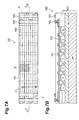
- Fig. 7A shows a top view of a prior-art full-frame transfer solid-state image pickup device (FFT CCD) or frame transfer (FT) CCD for the case of two-phase drive
- Fig. 7B shows a sectional view of the same along arrows IV-IV.
- a CCD 100 comprises a semiconductor substrate 101, transfer electrodes 102, set on a top surface side of semiconductor substrate 101, and supply wiring lines 103, electrically connected to transfer electrodes 102.
- a photosensitive part which picks up an image of light that is made incident on CCD 100, is arranged.
- the photosensitive part has a plurality of pixels E aligned in a horizontal direction and a vertical direction. By light being made incident on pixels E, charges are generated in the interiors of pixels E and image pickup of the image of light is carried out thereby.
- a predetermined number of transfer electrodes 102 are set on top of pixel E with their longitudinal direction being set along the horizontal direction of the photosensitive part and, by being supplied vertical transfer voltages, transfer charges in the vertical direction.
- Supply wiring lines 103 are the wiring for supplying the transfer voltages to the transfer electrodes 102 and are disposed, with their longitudinal direction being set along the vertical direction, at the respective end parts of CCD 100, which are dead zones F where an image of light is not picked up.
- a polycrystalline silicon (polysilicon) or other light transmitting material is used as the material of transfer electrodes 102.
- Supply wiring lines 103 which are formed of aluminum or other metal and are disposed at the respective ends of transfer electrodes 102, are used for supplying voltages to transfer electrodes 102.
- supply wiring lines 103 which are formed of aluminum, etc., block light
- supply wiring lines 103 are installed at dead zones F at the respective end parts of CCD 100 as described above.
- dead zones F are a problem in terms of making effective use of the surface of CCD 100, and thus dead zones F are preferably as small as possible.
- Such dead zones F also present problems in cases where a plurality of solid-state image pickup devices are aligned so as to be adjacent each other in the horizontal direction. That is, by dead zones F existing between the plurality of aligned solid-state image pickup elements, parts of an image of light will not be picked up.
- This invention has been made to resolve the above issues and an object thereof is to provide a solid-state image pickup device, with which dead zones can be made small and a photosensitive part can be made wide, and a solid-state image pickup device array that uses such solid-state image pickup devices.
- this invention provides a solid-state image pickup device comprising: a photosensitive part, having m ⁇ n pixels, formed on a semiconductor substrate, which includes a p-type semiconductor layer and an n-type semiconductor layer, and aligned two-dimensionally along m columns (where m is an integer of 2 or more), which partition a horizontal direction, and n rows (where n is an integer of 2 or more), which partition a vertical direction, and picking up an image of light that is made incident thereon; a transfer electrode, being installed on top of the pixels with the longitudinal direction thereof being set along the horizontal direction of the photosensitive part and being applied a vertical transfer voltage that transfers charges generated in the pixels in the vertical direction; and a supply wiring line, formed of metal or metal silicide, installed so as to cover a part of a light-shielded pixel, which is a predetermined pixel among the pixels, and with the longitudinal direction thereof being set along the vertical direction of the photosensitive part, being electrically connected to the transfer electrode, and
- the photosensitive part can be made wide. Also by eliminating the dead zones, parts at which image pickup cannot be performed can be lessened in cases where a plurality of the solid-state image pickup devices are used upon being made adjacent each other in the horizontal direction. Also, the supply wiring line is arranged to cover only a part of the light-shielded pixel.
- this invention's solid-state image pickup device array is characterized in that a plurality of the above-described solid-state image pickup devices are aligned in a mutually adjacent manner with the photosensitive parts aligned in the horizontal direction. Since the above-described solid-state image pickup device does not require dead zones for installing supply wiring lines, by aligning a plurality of the solid-state image pick-up devices, the intervals between the respective photosensitive parts can be made narrow. Non-image-pickup parts that exist in an image that has been picked up by the solid-state image pickup device array can thus be made small.
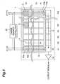
- Fig. 1 is a schematic arrangement diagram of a first embodiment of this invention's solid-state image pickup device as viewed from the top surface side.
- the solid-state image pickup device is equipped with a two-phase drive FFT CCD.
- This FFT CCD has an arrangement wherein charges, which are generated by the incidence of an image of light from the top surface side of a photosensitive part, are transferred in the photosensitive part.
- This solid-state image pickup device is arranged from a CCD 1, which is an FFT CCD, and a charge transfer control part 20.
- CCD 1 is equipped with a photosensitive part 10, a horizontal shift register 15, and an amplifying part 16.
- Photosensitive part 10 is divided in its horizontal direction into m columns H1 to Hm (where m is an integer of 2 or more), each having its longitudinal direction aligned along the vertical direction, and is divided in its vertical direction into n rows V1 to Vn (where n is an integer of 2 or more), each having its longitudinal direction aligned along the horizontal direction, and is thereby arranged from m ⁇ n pixels A.
- m is an integer of 2 or more
- V1 to Vn where n is an integer of 2 or more
- two or four transfer electrodes are installed for each row.
- supply wiring lines 13a and 13b are formed of aluminum or other metal or metal silicide of low electrical resistance and are installed on top of the pixels of columns H1 and Hm, which among the m columns are located at the respective ends of photosensitive part 10, so as to cover a part of each pixel.
- supply wiring lines 13a and 13b are installed in a manner such that one set of wiring lines, comprising the two wiring lines of one each of supply wiring lines 13a and 13b, is installed per column.
- Supply wiring line 13a is electrically connected to corresponding transfer electrode among the two to four transfer electrodes that are installed for each row Vj and supplies transfer voltage P1 to the transfer electrode.
- Supply wiring line 13b is likewise electrically connected to corresponding transfer electrode and supplies transfer voltage P2 to the transfer electrode.
- Horizontal shift register 15 receives the charges, which were generated in the respective pixels A and were transferred in the vertical direction of photosensitive part 10, from photosensitive part 10, transfers these charges in the horizontal direction (arrow b), and outputs the charges to amplifying part 16.
- the charges output from horizontal shift register 15 are amplified by amplifying part 16 and are then output to the exterior of the solid-state image pickup device as output signals according to the respective pixels.
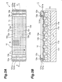
- Fig. 2A and Fig. 2B are (A) a top view and (B) a section along arrows I-I showing a part of the arrangement of CCD 1 of the solid-state image pickup device shown in Fig. 1.
- CCD 1, shown in Fig. 2A and Fig. 2B, comprises a semiconductor substrate 11, transfer electrodes 12a to 12d, supply wiring lines 13a and 13b, and an insulating layer 14.
- Semiconductor substrate 11 comprises a p + type semiconductor substrate 111, which is of a p + conduction type and serves as the base of semiconductor substrate 11, a p-type semiconductor layer 112, which is an epitaxial layer that is formed on the top surface side of p + type semiconductor substrate 111, and an n-type semiconductor layer 113 and a p + type semiconductor layer 114, which are formed further on the top surface side.
- N-type semiconductor layer 113 and p + type semiconductor layer 114 are disposed in alternating manner in the horizontal directions with the vertical direction of photosensitive part 10 being their longitudinal direction.
- N-type semiconductor layer 113 and p-type semiconductor layer 112 form a pn junction, and n-type semiconductor layer 113 serves as a photosensitive region that generates charges upon incidence of an image of light.
- P + -type semiconductor layer 114 form isolation regions C that separate the respective columns Hi.
- Supply wiring line 13a is electrically connected to transfer electrodes 12a and 12b and vertical transfer voltage P1 is supplied to transfer electrodes 12a and 12b.
- supply wiring line 13b is electrically connected to transfer electrodes 12c and 12d and vertical transfer voltage P2 is supplied to transfer electrodes 12c and 12d. That is, with respect to semiconductor substrate 11, the set of transfer electrodes 12a and 12b apply a vertical transfer voltage of one phase and the set of transfer electrodes 12c and 12d apply a vertical transfer voltage of another phase.
- insulating layer 14 which insulates semiconductor substrate 11, transfer electrodes 12a to 12d, and supply wiring lines 13a and 13b from each other, oxide films, etc., that transmit light are used.
- Supply wiring lines 13a and 13b are installed on the top surface of columns H1 and Hm of photosensitive part 10 with their longitudinal direction being set along the direction parallel to the respective columns Hi of photosensitive part 10. Also, a protruding part 131a is disposed at the semiconductor substrate 11 side of the supply wiring line 13a, and protruding part 131a is electrically connected to transfer electrodes 12a and 12b. Likewise, a protruding part 131b (not shown in Fig. 2B) is disposed at the semiconductor substrate 11 side of the supply wiring line 13b, and protruding part 131b is electrically connected to transfer electrodes 12c and 12d.
- the solid-state image pickup device of the present embodiment when an image of light is made incident from the top surface side of photosensitive part 10, the image of light is transmitted through transfer electrodes 12a to 12d and insulating layer 14 and reaches the interiors of the respective pixels A of photosensitive part 10. Charges are then generated in the interiors of the respective pixels A. These charges are held once in the interiors of pixels A and then transferred in the vertical direction by vertical transfer voltages P1 and P2 being applied to the corresponding transfer electrodes 12a to 12d and by these voltages being controlled by charge transfer control part 20. The transferred charges are then output to horizontal shift register 15. The charges are then transferred in the horizontal direction by horizontal shift register 15 and then input into and amplified by amplifying part 16. The amplified charges are output to the exterior of the solid-state image pickup device as output signals according to the respective pixels A.
- this embodiment's solid-state image pickup device provides the following effects. That is, supply wiring lines 13a and 13b, which are formed of a metal or metal silicide that blocks light and were priorly installed at dead zones at the respective ends of a CCD, are installed on top of pixels in the solid-state image pickup device of this embodiment. Since dead zones for installing supply wiring lines 13a and 13b can thus be eliminated from the respective ends of a CCD, photosensitive part 10 can be made wide in CCD 1.
- supply wiring lines 13a and 13b are arranged to cover just a part of each of light-shielded pixels D.
- light is made incident on the other parts of light-shielded pixels D and output signals, which are lowered in output amounts to some degree, are output from the light-shielded pixels D.
- the amount of lowering of the incident light amount on light-shielded pixels D can be corrected based on the output signals that are lowered in output amounts.
- Fig. 3A and Fig. 3B are tables showing (A) an example of output signal data from pixels A and (B) an example of output signal data from light-shielded pixels D and pixels A in an FFT CCD with 1024 columns and 64 rows.
- driving an FFT CCD by TDI drive which shall be described later, is equivalent to adding the signals of the 64 pixels in the vertical direction. It thus becomes adequate to correct the output signals for the 1024 channels in the horizontal direction that correspond to the respective columns.
- both the tables of Fig. 3A and Fig. 3B show variations of the output signals for the horizontal direction.
- the pixel Nos. shown in Fig. 3A indicate the channel Nos. in the horizontal direction.
- the output signals an example of the output signals of channels 1 to 4 and 1021 to 1024 is shown.
- the output signals of channels 5 to 1020 are omitted since these are substantially similar to those of channels 1 to 4 and channels 1021 to 1024.
- the pixel Nos. shown in Fig. 3B indicate the channel Nos. in the horizontal direction.
- the output signals an example of the output signals of channels 1 to 4 and 1021 to 1024 is shown.
- the supply wiring lines are installed on top of the top surfaces of the pixels of columns H2 and H3 and columns H1022 and H1023, and the pixels of all of the corresponding channels are light-shielded pixels.
- reference output signals which are the output signals obtained upon making a light of substantially uniform intensity incident on the photosensitive part. Then based on the reference output signals of the light-shielded pixels, the output signals of the same light-shielded pixels are corrected. Or, the output signals of light-shielded pixels may be corrected based on the reference output signals of pixels adjacent the light-shielded pixels.
- correction based on the output signals of the pixels adjacent the light-shielded pixels may be carried out without using reference output signals. That is, the output signals of the light-shielded pixels may be corrected using the correlation between the output signal values of the light-shielded pixels and the output signal values of the adjacent pixels that are not light-shielded pixels.
- a correction method there is a method wherein, based on reference output signals, a correction factor is computed such that the values obtained by multiplying the reference output signals of the light-shielded pixels by the correction factor become substantially equal to the values of the reference output signals of the pixels besides the light-shielded pixels, and in picking up an image of light, the output signals of the light-shielded-pixels, among the output signals obtained by the image pickup, are corrected by multiplying by the correction factor.
- the output signals of light-shielded pixels can be corrected readily.
- Such binning is especially effective in cases where the present solid-state image pickup device is to be applied to a device with which a problem will not arise even if the resolution is lowered.
- the resolution may be lower in comparison to visible light image pickup in many cases, and with panorama and cephalo x-ray image pickup devices used for treatment in dentistry, the resolution may be approximately 5 to 10Lp/mm.
- a resolution of approximately 2 to 5Lp/mm is sufficient.
- 2 to 5Lp/mm is a resolution, with which 2 to 5 black and white line pairs, drawn within a width of 1mm, can be defined. This corresponds to a pixel dimension of approximately 200 to 500 ⁇ m.
- a plurality of adjacent pixels can be handled as a unit pixel.
- the effects that the supply wiring lines have on the output signals of the unit pixels are thus lessened in comparison to those on the light-shielded pixels, and the output signals of the light-shielded pixels can be corrected favorably.
- the supply wiring lines should be installed so that the columns on which the supply wiring lines are installed will not be adjacent each other.
- supply wiring lines 13a and 13b are installed on pixels of columns at the respective ends of photosensitive part 10.
- vertical transfer voltages P1 and P2 can be applied efficiently onto transfer electrodes 12a to 12d from supply wiring lines 13a and 13b.
- supply wiring lines 13a and 13b at columns substantially at the center of photosensitive part 10, the same effects as those of the present embodiment can be obtained.
- the number of supply wiring lines will be the minimum necessary by the above configurations, the number of light-shielded pixels can be made low.
- Supply wiring lines 13a and 13b are installed as a set of two wiring lines for applying the two-phase vertical transfer voltages P1 and P2 and the two supply wiring lines that form a set are installed above a single column of pixels. By installing the supply wiring lines in this manner, the number of light-shielded pixels D, which are required per set of supply wiring lines and with which the output signals are corrected, can be made low.
- the TDI (Time Delay Integration) drive method can be cited as method of performing image pickup of image pickup subjects that move at a fixed velocity, such as objects on a belt conveyor, etc.
- TDI drive method while performing charge transfer between potential wells at a rate that is in accordance with the movement velocity of the image pickup subjects, further accumulation of charges is performed to thereby perform image pickup of moving images of light without blur.
- Such a drive method is realized by the control of vertical transfer voltages P1 and P2 by the abovementioned charge transfer control part 20.
- charge transfer control part 20 of the solid-state image pickup device performing such charge transfer by the TDI drive method, image pickup objects moving at a fixed velocity can be picked up clearly.
- This TDI drive method is also used often in the abovementioned panorama and cephalo X-ray image pickup devices as well.
- the effect of eliminating dead zones by the above-described arrangement becomes especially effective in a solid-state image pickup device array, wherein a plurality of the solid-state image pickup devices are aligned in a manner such that photosensitive parts 10 are aligned adjacent each other in the horizontal direction.
- Fig. 4 is a schematic arrangement diagram of a solid-state image pickup device array using this invention's solid-state image pickup devices as viewed from the top surface side.
- a plurality of CCDs 1, shown in Fig. 1 are aligned so as to be adjacent each other in the horizontal direction.
- an example of an X-ray image pickup device used for treatment in dentistry shall be described.
- a length of approximately 220mm is required as the length of an effective photosensitive region, which is a region in the solid-state image pickup device wherein image pickup is enabled, and with a panorama X-ray image pickup device, a length of approximately 150mm is required for the effective photosensitive region.
- a plurality of solid-state image pickup devices are thus aligned and set on a ceramic or printed circuit board to obtain the length required of the effective photosensitive region.
- the width of the dead zone at one end part of a photosensitive part is, for example, 100 ⁇ m and the width of the dead zone at the other end is 200 ⁇ m, a dead zone of 300 ⁇ m in total is formed at each seam between photosensitive parts. Due to these dead zones, non-image-pickup parts exist in a picked-up image and this can influence diagnosis in dentistry. The existence of non-image-pickup parts in a picked-up image is thus a problem with prior-art solid-state image pickup device arrays. However, by using the solid-state image pickup device array shown in Fig. 4, dead zones due to the installation of supply wiring lines are eliminated and the non-image-pickup parts can be made small.
- Fig. 5A and Fig. 5B are (A) a top view and (B) a section along arrows II-II showing a part of the arrangement of a CCD 2 of a solid-state image pickup device of a second embodiment.
- CCD 2 shown in Fig. 5A and Fig. 5B comprises a semiconductor substrate 11, transfer electrodes 12a to 12d, supply wiring lines 23a and 23b, and an insulating layer 14.
- transfer electrodes 12a to 12d supply wiring lines 23a and 23b
- insulating layer 14 the arrangement of parts besides supply wiring lines 23a and 23b are the same as those of the solid-state image pickup device of the first embodiment, description thereof shall be omitted.
- Supply wiring lines 23a and 23b are installed on the top surfaces of columns H1, Hm, and a substantially central column with their longitudinal direction being set along the direction parallel to the respective columns Hi of photosensitive part 10. Also, a protruding part 231a is disposed on the supply wiring line 23a and a protruding part 231b is disposed on the supply wiring line 23b, and via these protruding parts, vertical transfer voltage P1 is applied to transfer electrodes 12a and 12b and vertical transfer voltage P2 is applied to transfer electrodes 12c and 12d.
- supply wiring lines 23a and 23b are arranged to cover only a part of each light-shielded pixel D. The amount of lowering of the incident light amount on light-shielded pixels D can thus be corrected based on the output signals that are lowered in output amounts.
- a set of supply wiring lines 23a and 23b are installed on the top surface of the substantially central column of photosensitive part 10.
- the distances between supply wiring lines 23a mutually and the distances between supply wiring lines 23b mutually are thus shortened. Since the influence due to the electrical resistances of transfer electrodes 12a to 12d can thus be restrained at a low level, the charge transfer rate of CCD 2 can be made high and CCD 2 can be driven at high speed.
- Supply wiring lines 23a and 23b may be installed just on the top surface of the substantially central column of photosensitive part 10. By such installation, vertical transfer voltages P1 and P2 can be applied efficiently onto transfer electrodes 12a to 12d from supply wiring lines 23a and 23b. Also, since the number of supply wiring lines becomes the minimum necessary, the number of light-shielded pixels can be made low.
- Fig. 6A and Fig. 6B are (A) a top view and (B) a section along arrows III-III showing a part of the arrangement of a CCD 3 of a solid-state image pickup device of a third embodiment.
- CCD 3 shown in Fig. 6A and Fig. 6B comprises a semiconductor substrate 11, transfer electrodes 12a to 12d, supply wiring lines 33a and 33b, and an insulating layer 14.
- transfer electrodes 12a to 12d supply wiring lines 33a and 33b
- insulating layer 14 the arrangement of parts besides supply wiring lines 33a and 33b are the same as those of the solid-state image pickup device of the first embodiment, description thereof shall be omitted.
- Supply wiring lines 33a and 33b are installed on the top surfaces of arbitrary columns Hi on the top surface of insulating layer 14, with their longitudinal direction being set along the direction parallel to the respective columns Hi of photosensitive part 10.
- supply wiring lines 33a and 33b are installed on mutually different columns.
- a protruding part 331a is disposed on the supply wiring line 33a and a protruding part 331b is disposed on the supply wiring line 33b, and via these protruding parts, vertical transfer voltage P1 is applied to transfer electrodes 12a and 12b and vertical transfer voltage P2 is applied to transfer electrodes 12c and 12d.
- supply wiring lines 33a and 33b are arranged to cover only a part of each light-shielded pixel D. The amount of lowering of the incident light amount on light-shielded pixels D can thus be corrected based on the output signals that are lowered in output amounts.
- supply wiring lines 33a and 33b the two supply wiring lines that form a set for applying the two-phase vertical transfer voltages P1 and P2 are installed on top of pixels of mutually different columns.
- the supply wiring lines being installed in this manner, the area covered by supply wiring lines of each light-shielded pixel is lessened and the lowering of the incident light amount onto the light-shielded pixels is thus made small. The correction of the output signals of the light-shielded pixels can thereby be facilitated.
- This invention's solid-state image pickup device is not restricted to the above-described embodiments and various modifications are possible.
- an arbitrary number thereof may be installed on the top surfaces of pixels at arbitrary locations besides those of the above-described embodiments and may thus be designed as suitable according to the required charge transfer rate, correction method, etc.
- a two-phase drive CCD is used. Besides this, even when a CCD of three-phase drive or higher is used, a solid-state image pickup device by this invention can be arranged favorably by installing the required number of supply wiring lines on top of pixels.
- an FFT CCD is used as the CCD
- another type of CCD may be used instead.
- FT CCD frame transfer type CCD
- This invention's solid-state image pickup device and solid-state image pickup device array can be used as a solid-state image pickup device and solid-state image pickup device array, with which the dead zones can be made small and the photosensitive parts can be made wide. That is, with the solid-state image pickup device, since by the installing of supply wiring lines, which are formed of light-blocking material, on top of pixels, the dead zones for installing supply wiring lines, which existed at the respective end parts in the horizontal direction of the photosensitive part in the prior art, can be eliminated, the photosensitive part can be made wide. Also by eliminating the dead zones of the solid-state image pickup device, parts at which image pickup is not performed can be lessened in cases where a plurality of the solid-state image pickup devices are used adjacent each other in the horizontal direction.
- the supply wiring lines are arranged to cover only a part of the light-shielded pixels. Since light is made incident on the other parts of the light-shielded pixels, output signals, which are lowered to some degree in output amount, are output from the light-shielded pixels. Thus with the solid-state image pickup device of the above arrangement, the lowering of the incident light amount on the light-shielded pixels can be corrected based on the output signal.
Landscapes
- Solid State Image Pick-Up Elements (AREA)
- Transforming Light Signals Into Electric Signals (AREA)
Abstract
Description
Claims (10)
- A solid-state image pickup device comprising:wherein being arranged to enable correction of the amount of lowering of an output signal, output by said light-shielded pixel, due to said supply wiring line.a photosensitive part, having m × n pixels, formed on a semiconductor substrate, which includes a p-type semiconductor layer and an n-type semiconductor layer, and aligned two-dimensionally along m columns (where m is an integer of 2 or more), which partition a horizontal direction, and n rows (where n is an integer of 2 or more), which partition a vertical direction, and picking up an image of light that is made incident thereon;a transfer electrode, being installed on top of said pixels with the longitudinal direction thereof being set along the horizontal direction of said photosensitive part and being applied a vertical transfer voltage that transfers charges generated in said pixels in the vertical direction; anda supply wiring line, formed of metal or metal silicide, installed so as to cover a part of a light-shielded pixel, which is a predetermined pixel among said pixels, and with the longitudinal direction thereof being set along the vertical direction of said photosensitive part, being electrically connected to said transfer electrode, and applying said vertical transfer voltage to said transfer electrode;
- The solid-state image pickup device according to Claim 1, wherein said supply wiring lines are installed on top of said pixels of columns, among said m columns, at the respective ends of said photosensitive part.
- The solid-state image pickup device according to Claim 1 or 2, wherein said supply wiring line is installed on top of said pixels of a substantially central column, among said m columns of said photosensitive part.
- The solid-state image pickup device according to any of Claims 1 to 3, wherein said supply wiring line is installed as a set of k supply wiring lines for applying said vertical transfer voltages of k phases and the k said supply wiring lines that form a set are installed on top of said pixels of one column.
- The solid-state image pickup device according to any of Claims 1 to 3, wherein said supply wiring line is installed as a set of k supply wiring lines for applying said vertical transfer voltages of k phases and the k said supply wiring lines that form a set are installed in a dispersed manner along a plurality of columns.
- The solid-state image pickup device according to any one of Claims 1 to 5, wherein light of substantially uniform intensity is made incident in advance on said photosensitive part to determine a reference output signal and the output signal of said light-shielded pixel is corrected based on said reference output signal.
- The solid-state image pickup device according to any one of Claims 1 to 6, wherein the output signal of said light-shielded pixel is corrected based on the output signal of said pixel adjacent said light-shielded pixel.
- The solid-state image pickup device according to any one of Claims 1 to 7, wherein binning, in which the charges generated in a predetermined number of said pixels are added to form an output signal, is performed.
- The solid-state image pickup device according to any one of Claims 1 to 8, wherein said vertical transfer voltage is controlled by the TDI drive method, in which charges are transferred in the vertical direction at a rate corresponding to the movement velocity of an image pickup subject to perform image pickup without blur of said image of light of said image pickup subject.
- A solid-state image pickup device array wherein a plurality of the solid-state image pickup devices according to any one of Claims 1 to 9 are aligned in a mutually adjacent manner with said photosensitive parts being aligned in the horizontal direction.
Applications Claiming Priority (3)
| Application Number | Priority Date | Filing Date | Title |
|---|---|---|---|
| JP2002153035A JP4246964B2 (en) | 2002-05-27 | 2002-05-27 | Solid-state imaging device and solid-state imaging device array |
| JP2002153035 | 2002-05-27 | ||
| PCT/JP2003/005610 WO2003100862A1 (en) | 2002-05-27 | 2003-05-02 | Solid-state imaging device and solid-state imaging device array |
Publications (3)
| Publication Number | Publication Date |
|---|---|
| EP1515370A1 true EP1515370A1 (en) | 2005-03-16 |
| EP1515370A4 EP1515370A4 (en) | 2006-03-15 |
| EP1515370B1 EP1515370B1 (en) | 2009-04-01 |
Family
ID=29561286
Family Applications (1)
| Application Number | Title | Priority Date | Filing Date |
|---|---|---|---|
| EP03725732A Expired - Lifetime EP1515370B1 (en) | 2002-05-27 | 2003-05-02 | Solid-state imaging device and solid-state imaging device array |
Country Status (6)
| Country | Link |
|---|---|
| US (1) | US7193252B2 (en) |
| EP (1) | EP1515370B1 (en) |
| JP (1) | JP4246964B2 (en) |
| AU (1) | AU2003231373A1 (en) |
| DE (1) | DE60326955D1 (en) |
| WO (1) | WO2003100862A1 (en) |
Cited By (1)
| Publication number | Priority date | Publication date | Assignee | Title |
|---|---|---|---|---|
| EP1571830A3 (en) * | 2004-02-27 | 2007-08-22 | Rigaku Corporation | Method for CCD sensor control, CCD sensor system and X-ray diffraction apparatus |
Families Citing this family (10)
| Publication number | Priority date | Publication date | Assignee | Title |
|---|---|---|---|---|
| JP4714502B2 (en) * | 2005-04-26 | 2011-06-29 | パナソニック株式会社 | Solid-state imaging device |
| US20060267059A1 (en) * | 2005-05-25 | 2006-11-30 | Macronix International Co., Ltd. | Peripheral circuit architecture for array memory |
| JP4731278B2 (en) * | 2005-10-25 | 2011-07-20 | パナソニック株式会社 | Method for driving solid-state imaging device |
| JP5000258B2 (en) * | 2006-10-18 | 2012-08-15 | 浜松ホトニクス株式会社 | Solid-state imaging device |
| JP5470928B2 (en) | 2009-03-11 | 2014-04-16 | ソニー株式会社 | Method for manufacturing solid-state imaging device |
| JP2011056170A (en) * | 2009-09-14 | 2011-03-24 | Fujifilm Corp | Radiographic system and method of controlling the same |
| JP6110154B2 (en) | 2013-02-13 | 2017-04-05 | 浜松ホトニクス株式会社 | Solid-state imaging device and method for manufacturing solid-state imaging device |
| US10903258B2 (en) * | 2017-10-11 | 2021-01-26 | Kla Corporation | Image sensors with grounded or otherwise biased channel-stop contacts |
| JP6788648B2 (en) * | 2018-10-24 | 2020-11-25 | キヤノン株式会社 | Radiography equipment, radiography methods and programs |
| EP4358505B1 (en) * | 2021-07-13 | 2026-05-27 | Hamamatsu Photonics K.K. | X-ray image acquisition device and x-ray image acquisition system |
Family Cites Families (22)
| Publication number | Priority date | Publication date | Assignee | Title |
|---|---|---|---|---|
| JPS57188183A (en) * | 1981-05-15 | 1982-11-19 | Canon Inc | Solid-state image pickup device |
| US4689687A (en) * | 1984-11-13 | 1987-08-25 | Hitachi, Ltd. | Charge transfer type solid-state imaging device |
| JPS62220807A (en) * | 1986-03-20 | 1987-09-29 | Toshiba Corp | star sukyana |
| US4972254A (en) * | 1987-02-24 | 1990-11-20 | Kabushiki Kaisha Toshiba | Solid state image sensors for reproducing high definition images |
| JP2880026B2 (en) * | 1992-08-28 | 1999-04-05 | 富士写真フイルム株式会社 | CCD imaging device and driving method thereof |
| JP3203060B2 (en) | 1992-08-28 | 2001-08-27 | 浜松ホトニクス株式会社 | Radiation detector |
| US5483090A (en) * | 1993-04-09 | 1996-01-09 | Sanyo Electric Co., Ltd. | Solid-state image pickup device and method for manufacturing such device |
| JP3310404B2 (en) * | 1993-07-23 | 2002-08-05 | 浜松ホトニクス株式会社 | Cooling type solid-state imaging device |
| JP2701726B2 (en) * | 1993-12-28 | 1998-01-21 | 日本電気株式会社 | Solid-state imaging device |
| JP3334992B2 (en) * | 1994-02-22 | 2002-10-15 | 浜松ホトニクス株式会社 | CCD solid-state imaging device and manufacturing method |
| US5530475A (en) * | 1994-11-30 | 1996-06-25 | Eastman Kodak Company | Image sensor with oversized vertical shift registers for marker pixel generation |
| US5821547A (en) * | 1997-03-10 | 1998-10-13 | Talmi; Yair | Temporal filter using interline charged coupled device |
| DE19818975A1 (en) * | 1997-08-12 | 1999-02-18 | Hewlett Packard Co | Method for correcting dark current in CMOS imaging sensors |
| JP3426935B2 (en) * | 1997-10-21 | 2003-07-14 | 三洋電機株式会社 | Solid-state imaging device and method of manufacturing solid-state imaging device |
| JP4271753B2 (en) * | 1998-09-21 | 2009-06-03 | 浜松ホトニクス株式会社 | Solid-state imaging device |
| JP2000069373A (en) * | 1999-08-23 | 2000-03-03 | Hamamatsu Photonics Kk | CCD solid-state imaging device |
| DE60045484D1 (en) * | 1999-09-30 | 2011-02-17 | Shimadzu Corp | ULTRA-FAST PICTURE RECEIVER |
| EP1102323B1 (en) | 1999-11-19 | 2012-08-15 | CSEM Centre Suisse d'Electronique et de Microtechnique SA - Recherche et Développement | Method for detecting electromagnetic radiation using an optoelectronic sensor |
| US6744526B2 (en) * | 2001-02-09 | 2004-06-01 | Eastman Kodak Company | Image sensor having black pixels disposed in a spaced-apart relationship from the active pixels |
| JP2002289822A (en) * | 2001-03-23 | 2002-10-04 | Hamamatsu Photonics Kk | X-ray CCD |
| US7218351B2 (en) * | 2002-04-05 | 2007-05-15 | Victor Company Of Japan, Limited | Image-sensing apparatus for compensating video signal of a plurality of channels |
| US9386241B2 (en) * | 2003-07-02 | 2016-07-05 | Verity Instruments, Inc. | Apparatus and method for enhancing dynamic range of charge coupled device-based spectrograph |
-
2002
- 2002-05-27 JP JP2002153035A patent/JP4246964B2/en not_active Expired - Lifetime
-
2003
- 2003-05-02 US US10/515,548 patent/US7193252B2/en not_active Expired - Lifetime
- 2003-05-02 WO PCT/JP2003/005610 patent/WO2003100862A1/en not_active Ceased
- 2003-05-02 DE DE60326955T patent/DE60326955D1/en not_active Expired - Lifetime
- 2003-05-02 EP EP03725732A patent/EP1515370B1/en not_active Expired - Lifetime
- 2003-05-02 AU AU2003231373A patent/AU2003231373A1/en not_active Abandoned
Cited By (1)
| Publication number | Priority date | Publication date | Assignee | Title |
|---|---|---|---|---|
| EP1571830A3 (en) * | 2004-02-27 | 2007-08-22 | Rigaku Corporation | Method for CCD sensor control, CCD sensor system and X-ray diffraction apparatus |
Also Published As
| Publication number | Publication date |
|---|---|
| JP2003347539A (en) | 2003-12-05 |
| US20050151169A1 (en) | 2005-07-14 |
| US7193252B2 (en) | 2007-03-20 |
| DE60326955D1 (en) | 2009-05-14 |
| JP4246964B2 (en) | 2009-04-02 |
| WO2003100862A1 (en) | 2003-12-04 |
| EP1515370B1 (en) | 2009-04-01 |
| AU2003231373A1 (en) | 2003-12-12 |
| EP1515370A4 (en) | 2006-03-15 |
Similar Documents
| Publication | Publication Date | Title |
|---|---|---|
| US20100194946A1 (en) | Solid-state image pickup apparatus and camera | |
| KR102542664B1 (en) | Solid-state imaging device, driving method therefor, and electronic apparatus | |
| CN103650479B (en) | Solid-state imaging device, driving method thereof, manufacturing method, and electronic device | |
| US10658404B2 (en) | Solid state imaging device and imaging apparatus with pixel column having multiple output lines | |
| EP1515370B1 (en) | Solid-state imaging device and solid-state imaging device array | |
| KR101575378B1 (en) | Solid-state imager and x-ray ct apparatus including same | |
| US10685991B2 (en) | Solid-state imaging device | |
| US10048380B2 (en) | Distance-measuring imaging device and solid state imaging element | |
| TWI795796B (en) | Solid camera device, signal processing method of solid camera device, and electronic apparatus | |
| JP2002270809A (en) | Solid-state imaging device and control method thereof | |
| JP3697827B2 (en) | Flat panel type sensor | |
| US7847848B2 (en) | Solid-state imaging device having a plurality of lines formed in at least two layers on semiconductor substrate | |
| US5990503A (en) | Selectable resolution CCD sensor | |
| JP2004129256A (en) | Method for reducing dark current of charge-coupled device in accumulation mode | |
| US7804539B2 (en) | Solid-state imaging device and method of driving same | |
| US10397501B2 (en) | Solid-state image sensor and imaging apparatus | |
| US7589775B2 (en) | Solid-state imaging device | |
| KR100871163B1 (en) | Solid-state imaging device | |
| US7595517B2 (en) | Charge coupled device having diverged channel | |
| JP3592772B2 (en) | Solid-state imaging device | |
| US5929471A (en) | Structure and method for CCD sensor stage selection | |
| JP3397151B2 (en) | Driving method of solid-state imaging device | |
| CN100468761C (en) | Solid-state imaging device and its driving and manufacturing method, camera and its driving method | |
| JP4271753B2 (en) | Solid-state imaging device | |
| JPH06151806A (en) | Solid-state imaging device |
Legal Events
| Date | Code | Title | Description |
|---|---|---|---|
| PUAI | Public reference made under article 153(3) epc to a published international application that has entered the european phase |
Free format text: ORIGINAL CODE: 0009012 |
|
| 17P | Request for examination filed |
Effective date: 20041216 |
|
| AK | Designated contracting states |
Kind code of ref document: A1 Designated state(s): AT BE BG CH CY CZ DE DK EE ES FI FR GB GR HU IE IT LI LU MC NL PT RO SE SI SK TR |
|
| AX | Request for extension of the european patent |
Extension state: AL LT LV MK |
|
| DAX | Request for extension of the european patent (deleted) | ||
| RBV | Designated contracting states (corrected) |
Designated state(s): DE FI FR IT |
|
| A4 | Supplementary search report drawn up and despatched |
Effective date: 20060130 |
|
| 17Q | First examination report despatched |
Effective date: 20060310 |
|
| GRAP | Despatch of communication of intention to grant a patent |
Free format text: ORIGINAL CODE: EPIDOSNIGR1 |
|
| GRAS | Grant fee paid |
Free format text: ORIGINAL CODE: EPIDOSNIGR3 |
|
| GRAA | (expected) grant |
Free format text: ORIGINAL CODE: 0009210 |
|
| AK | Designated contracting states |
Kind code of ref document: B1 Designated state(s): DE FI FR IT |
|
| REF | Corresponds to: |
Ref document number: 60326955 Country of ref document: DE Date of ref document: 20090514 Kind code of ref document: P |
|
| PLBE | No opposition filed within time limit |
Free format text: ORIGINAL CODE: 0009261 |
|
| STAA | Information on the status of an ep patent application or granted ep patent |
Free format text: STATUS: NO OPPOSITION FILED WITHIN TIME LIMIT |
|
| 26N | No opposition filed |
Effective date: 20100105 |
|
| REG | Reference to a national code |
Ref country code: FR Ref legal event code: PLFP Year of fee payment: 14 |
|
| REG | Reference to a national code |
Ref country code: FR Ref legal event code: PLFP Year of fee payment: 15 |
|
| REG | Reference to a national code |
Ref country code: FR Ref legal event code: PLFP Year of fee payment: 16 |
|
| PGFP | Annual fee paid to national office [announced via postgrant information from national office to epo] |
Ref country code: IT Payment date: 20220412 Year of fee payment: 20 Ref country code: FR Payment date: 20220408 Year of fee payment: 20 Ref country code: DE Payment date: 20220329 Year of fee payment: 20 |
|
| PGFP | Annual fee paid to national office [announced via postgrant information from national office to epo] |
Ref country code: FI Payment date: 20220509 Year of fee payment: 20 |
|
| REG | Reference to a national code |
Ref country code: DE Ref legal event code: R071 Ref document number: 60326955 Country of ref document: DE |
|
| P01 | Opt-out of the competence of the unified patent court (upc) registered |
Effective date: 20230509 |