EP1515360B1 - Method and apparatus for manipulating a microscopic sample - Google Patents
Method and apparatus for manipulating a microscopic sample Download PDFInfo
- Publication number
- EP1515360B1 EP1515360B1 EP04076630A EP04076630A EP1515360B1 EP 1515360 B1 EP1515360 B1 EP 1515360B1 EP 04076630 A EP04076630 A EP 04076630A EP 04076630 A EP04076630 A EP 04076630A EP 1515360 B1 EP1515360 B1 EP 1515360B1
- Authority
- EP
- European Patent Office
- Prior art keywords
- sample
- sample carrier
- wire
- carrier
- separation
- Prior art date
- Legal status (The legal status is an assumption and is not a legal conclusion. Google has not performed a legal analysis and makes no representation as to the accuracy of the status listed.)
- Expired - Lifetime
Links
- 238000000034 method Methods 0.000 title claims description 24
- 238000000926 separation method Methods 0.000 claims description 21
- 239000000758 substrate Substances 0.000 claims description 19
- 239000002245 particle Substances 0.000 claims description 8
- 235000012431 wafers Nutrition 0.000 description 17
- 238000004458 analytical method Methods 0.000 description 12
- 230000008878 coupling Effects 0.000 description 6
- 238000010168 coupling process Methods 0.000 description 6
- 238000005859 coupling reaction Methods 0.000 description 6
- 230000008901 benefit Effects 0.000 description 5
- 238000005520 cutting process Methods 0.000 description 5
- 238000010884 ion-beam technique Methods 0.000 description 5
- 230000007246 mechanism Effects 0.000 description 5
- 238000001465 metallisation Methods 0.000 description 4
- 239000000969 carrier Substances 0.000 description 3
- 238000004519 manufacturing process Methods 0.000 description 2
- 239000002184 metal Substances 0.000 description 2
- 239000004065 semiconductor Substances 0.000 description 2
- 230000005540 biological transmission Effects 0.000 description 1
- 230000008859 change Effects 0.000 description 1
- 238000000605 extraction Methods 0.000 description 1
- 239000011888 foil Substances 0.000 description 1
- 238000003384 imaging method Methods 0.000 description 1
- 238000003801 milling Methods 0.000 description 1
- 230000009467 reduction Effects 0.000 description 1
Images


Classifications
-
- G—PHYSICS
- G01—MEASURING; TESTING
- G01N—INVESTIGATING OR ANALYSING MATERIALS BY DETERMINING THEIR CHEMICAL OR PHYSICAL PROPERTIES
- G01N1/00—Sampling; Preparing specimens for investigation
- G01N1/28—Preparing specimens for investigation including physical details of (bio-)chemical methods covered elsewhere, e.g. G01N33/50, C12Q
- G01N1/32—Polishing; Etching
-
- H—ELECTRICITY
- H01—ELECTRIC ELEMENTS
- H01J—ELECTRIC DISCHARGE TUBES OR DISCHARGE LAMPS
- H01J2237/00—Discharge tubes exposing object to beam, e.g. for analysis treatment, etching, imaging
- H01J2237/20—Positioning, supporting, modifying or maintaining the physical state of objects being observed or treated
-
- H—ELECTRICITY
- H01—ELECTRIC ELEMENTS
- H01J—ELECTRIC DISCHARGE TUBES OR DISCHARGE LAMPS
- H01J2237/00—Discharge tubes exposing object to beam, e.g. for analysis treatment, etching, imaging
- H01J2237/26—Electron or ion microscopes
- H01J2237/28—Scanning microscopes
Definitions
- the invention relates to a method of manipulating a microscopic sample to be extracted from a substrate, whereby the manipulating movements are conducted with the aid of a manipulation system consisting of a sample carrier and a manipulator, which method comprises the following steps:
- the invention also relates to a particle-optical apparatus for performing this method.
- Such methods are principally used in the semiconductor industry, where samples of microscopic dimensions are removed from substrates such as wafers so as to make analyses and/or processing steps possible.
- samples have dimensions of the order of magnitude of 10 ⁇ m at a thickness of 100 ⁇ m.
- the analyses can, for example, be conducted with the aid of a TEM (Transmission Electron Microscope), SEM (Scanning Electron Microscope), SIMS (Secondary Ion Mass Spectroscope) or X-ray analytical apparatus.
- the further processing steps may, for example, comprise thinning the sample with the aid of an ion beam as part of an analysis with the aid of a TEM.
- a sample carrier in the form of a needle is moved on a manipulator to a position on a substrate where a sample is to be extracted from a substrate.
- the sample is attached to the extremity of the needle-shaped sample carrier by means of metal deposition.
- the sample attached to the manipulator is brought to another position with the aid of the manipulator.
- the sample is subsequently fixed to a carrier in the form of a TEM grid with the aid of metal deposition.
- the TEM grid has hollows and the sample is attached to the edge of such a hollow.
- a TEM grid consists of a metal foil in which hollows are created that are bordered by bars of said metal. It usually has an external diameter of the order of magnitude of 3 mm, hollows of 15 ⁇ m or larger, bordered by bars with a width of 10 ⁇ m or more and a thickness of 10 ⁇ m or more. Depending on the chosen embodiment of a TEM grid, the hollows may be up to hundreds of ⁇ m in size.
- a disadvantage of the known method is that the sample mounted on the sample carrier has to be positioned with sub-micron accuracy on the TEM grid by the manipulation system, so as to connect the comer points of the sample to the edge of the hollow without hindering the spatial accessibility of the sample during further processing and/or analysis.
- the sample has a size comparable to or smaller than the width of the bars of the TEM grid.
- Another disadvantage of the described method is that it does not offer the possibility of processing or analyzing the sample in apparatus that requires another grid or holder than that on which the sample is affixed.
- a further disadvantage lies in the determination of the position of the sample on the TEM grid, whereby, somewhere on the TEM grid - with a size of the order of magnitude of 3 mm and with hundreds of hollows - the microscopic sample - with a size of the order of magnitude of 10 ⁇ m - is fixed to a bar.
- the invention aims to provide a method that better facilitates manipulation of the microscopic sample according to claim 1.
- Remounting of the sample can occur by release, manipulation and mounting of the sample carrier, which is easier and more effective than release, manipulation and mounting of the microscopic sample. Such remounting may be necessary so as to change the position or orientation of the sample in the case of initially erroneous placement, or so as to mount the sample on another grid or another holder for use in apparatus in which the sample is to undergo subsequent processing or analysis.
- positional determination of the microscopic sample attached to the (relatively large) sample carrier is easier than positional determination of the sample without sample carrier: one first determines the position of the sample carrier and one then localizes the sample attached thereto by following the form of the sample carrier.
- Japanese publication JP2000155081A describes a particle-optical apparatus in which a sample is cut with an ion beam from a substrate and attached to a sample carrier.
- the sample carrier is removably attached to a manipulator. After attaching the sample to the sample carrier the manipulator moves the sample carrier to a sample holder, such as a TEM sample holder.
- the removable sample carrier is there mounted on the sample holder and detached from the manipulator.
- the sample carrier itself comprises a coupling mechanism and a tilted rod to which the sample is attached.
- US patent US6,188,068B1 describes a method in which a sample is formed from a substrate by focused ion beam milling, and a sample carrier for TEM imaging (the support fixture) is attached to the sample. The sample carrier is moved and positioned with a manipulator. Thereafter the sample mounted on the sample carrier is freed from the substrate and moved away from the substrate. US patent US6,188,068B1 does not disclose whether and how the sample carrier is separated from the manipulator.
- the sample carrier is formed by an end portion of a supply of wire, and the separation is applied by separating the end portion of the supply of wire from the supply of wire.
- An attendant advantage of this is that the remaining end of the supply of wire can - in the case of repeated application of the method - now be used as a new end portion of a subsequent sample carrier. Separation can comprise stretching the wire of the supply of wire in such a manner that constriction of the wire occurs, which has the advantage that the newly formed end of the supply of wire has a smaller diameter than the rest of the sample carrier, which simplifies placement of that end upon the microscopic sample to be removed.
- a sample carrier which has a rod-like extremity and the sample being attached to the sample carrier at an extremity of the sample carrier has the advantage that visibility at the location where the extremity of the relatively large sample carrier is attached to the microscopic sample is blocked as little as possible by the sample carrier itself, as a result of which the positioning of the extremity of the sample carrier upon the sample to be removed, before the sample is cut loose, is made as simple as possible.
- the sample carrier is detachably coupled to the manipulator.
- the manipulator - in an automated manner, and thus without human intervention - can remove the sample carrier from, for example, a cassette and, after attachment of the sample to the sample carrier and cutting loose of the sample, can place and release the sample carrier with attached sample into the same or another cassette, after which this cassette can be removed from the apparatus in which this method is performed, so as to allow the samples present in the cassette to undergo processing and/or analyses.
- the sample carrier can have a form that is suitable for use in apparatus for performing analyses and/or processing subsequent to extraction of the sample.
- the sample carrier can hold multiple samples, which can shorten the time necessary for analysis and/or processing. It is also possible to provide the sample carrier with a unique identification code, which simplifies identification of the sample during subsequent analyses and/or processing.
- This example of the apparatus is principally advantageous in environments where large numbers of samples are analyzed, such as in production environments for integrated circuits.
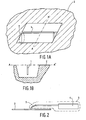
- Figures 1A and 1B show a substrate 2 in the form of a wafer containing a partially cut loose sample 1.
- the cutting loose of the sample can occur in a known manner with an ion beam.
- the underside of the sample 1 is already cut loose, and the sample is only connected to the wafer 2 via the connection 7 between wafer 2 and sample 1.
- the sample 1 nowadays has dimensions of the order of magnitude of 10 ⁇ m (i.e. length perpendicular to the line AA') at a thickness (i.e. dimension in the direction of the line AA') of 100 nm.
- the wafer 2 nowadays has a diameter of 300 mm, and it should be possible to take the sample from any random location on the wafer.
- Figure 1B shows a transverse cross-section according to the line AA' depicted in figure 1A , in which it can clearly be seen that the underside of sample 1 is free from the wafer 2.
- Figure 2 schematically shows a manipulator system 5, consisting of a manipulator 4 and a sample carrier 3.
- the manipulator 4 is able to move the sample carrier 3 within the plane of the wafer 2 to the position of the sample 1 to be removed from the wafer 2 (see figure 1A ) and also perpendicular thereto. In view of the dimensions of the sample 1, this will have to occur with an accuracy of the order of magnitude of 1 ⁇ m.
- Manipulators for positioning wafers with this type of accuracy are known per se.
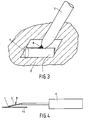
- Figure 3 schematically shows an extremity of the sample carrier 3 (see figure 2 ), which is connected to the manipulator 4 (see figure 2 ) and which is attached to the sample 1, whereby the connection 6 is in the form of a metal deposition. After cutting loose the connection 7 between the sample 1 and the wafer 2 with a particle beam, the sample 1 is only carried by the sample carrier 3.
- Figure 4 schematically shows the manipulator 4, which is positioning the sample carrier 3 (connected thereto) - and the sample 1 attached thereto - above a TEM grid 14.
- the sample carrier 3 is positioned above the TEM grid 14 by the manipulator 4 in such a manner that the sample 1, after separation, is located entirely within one of the hollows of the TEM grid 14 and the sample carrier 3 comes to rest upon one or more of the bars of the TEM grid 14, such as is further depicted in figure 5 .
- Subsequently - using, for example, a laser or particle beam - a separation is applied between the manipulator 4 and the sample carrier 3 at a position 8, whereby the portion of the sample carrier 3 that protrudes with respect to the sample 1 and that remains connected to the sample 1 is large with respect to the sample 1.
- Figure 5 schematically shows the positioning of the sample 1 after a separation has been applied between the sample carrier 3 and the manipulator 4.
- the sample carrier 3 rests upon one bar of the TEM grid 14 and the sample 1 is located entirely within a hollow 17 of the TEM grid 14, as a result of which the sample 1 is easily accessible for the purpose of processing and/or analysis in other apparatus.
- Figure 6 schematically shows an embodiment of the manipulator system 5, whereby the sample carrier 3 (see figure 2 ) is formed by the end portion 9 of a supply 11 of wire.
- separation means 15 are schematically shown here, which means 15 may be mechanical in nature - as will be explained further in figure 7 - but which may also be embodied as severing means that perform the separation with the aid of a laser or particle beam.
- Use of the supply 11 of wire makes it possible, in the case of repeated application of the method, to produce sample carriers 3 in a simple manner.
- the sample carrier 3, and thus the wire from which the sample carrier 3 is formed, should be very thin, in view of the dimensions of the sample 1 upon which the sample carrier 3 is positioned. In this context, one might consider wire such as that used in the semiconductor industry for "bonding" chips, which wire can have a diameter nowadays of 10 ⁇ m.
- Figure 7A schematically shows an embodiment of the mechanical separation means referred to with regard to figure 6 , whereby the end portion 9 is mechanically severed from the supply 11 of wire using knives 16 operating toward one another.
- Figure 7B schematically shows an embodiment of the mechanical separation means referred to with regard to figure 6 , whereby the end portion 9 is mechanically severed from the supply 11 of wire by means of stretching of the supply 11 of wire, achieved by moving apart the clamps 12, as a result of which constriction of the wire of the supply 11 of wire occurs.
- the constriction will have a diameter much smaller than the diameter of the end portion 9, so that the needle-like extremity of the end portion 9 to be newly formed as a result of this constriction will also be much thinner than the diameter of the wire of the supply 11 of wire, so that positioning upon the microscopic sample 1 is facilitated.
- Figure 8 shows - in a front elevation and also in a transverse cross-section according to line AA' - a sample carrier 3 that can be detachably coupled to the manipulator 4 already shown in figure 2 .
- the sample carrier 3 is formed from a relatively thick body 18, which the manipulator 4 can grip for the purpose of coupling, and tapering fingers 19 for attachment of samples 1.
- the form of the sample carrier 3 is chosen in such a manner that it is possible to use it in standard specimen carriers in apparatus in which processing and/or analysis are performed. These may be specimen carriers for use with TEM grids for application in TEM apparatus.
- the sample carrier 3 is embodied to carry several samples 1, thanks to the presence of several fingers 19.
- sample carrier 3 is provided with a (unique) identification code 13, which, during subsequent analyses and/or processing, facilitates identification of the samples attached to the sample carrier 3. This identification is of particular advantage in environments in which large numbers of samples are analyzed, such as in environments for the production of integrated circuits.
- FIG 8B schematically shows a sample carrier 3 such as shown in figure 8A , which is coupled to a manipulator 4 with the aid of a coupling mechanism 10, which coupling mechanism 10 is part of the manipulator 4.
- the mouth of this coupling mechanism 10 is closed using an actuator that is not depicted, whereby the sample carrier 3 becomes clamped.
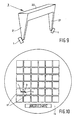
- FIG 9 schematically shows another example of a detachable sample carrier 3, which, in turn, is attached to a flat holder with one or more hollows 17 - such as a TEM grid 14 - such as is further depicted in figure 10 .
- This sample carrier 3 has a U form with a relatively thick middle portion 20 and thin legs 21.
- the relatively thick middle portion 20 can be gripped by a coupling mechanism 10 such as that shown in figure 8B .
- the sample 1 is attached to the thin legs 21.
- Figure 10 schematically shows the sample carrier 3 such as shown in figure 9 attached to a flat holder in the form of a TEM grid 14 with hollows 17, whereby the samples 1 connected to the sample carrier 3 both lie freely within a hollow 17.
- the TEM grid 14 is provided with a unique identification code 13.
Landscapes
- Physics & Mathematics (AREA)
- Health & Medical Sciences (AREA)
- Life Sciences & Earth Sciences (AREA)
- Chemical & Material Sciences (AREA)
- Analytical Chemistry (AREA)
- Biochemistry (AREA)
- General Health & Medical Sciences (AREA)
- General Physics & Mathematics (AREA)
- Immunology (AREA)
- Pathology (AREA)
- Sampling And Sample Adjustment (AREA)
- Manipulator (AREA)
Description
- The invention relates to a method of manipulating a microscopic sample to be extracted from a substrate, whereby the manipulating movements are conducted with the aid of a manipulation system consisting of a sample carrier and a manipulator, which method comprises the following steps:
- attaching the sample to the sample carrier and completely severing the sample from the substrate, and;
- subsequently applying a separation to the sample and the manipulator.
- The invention also relates to a particle-optical apparatus for performing this method.
- Such a method is known from US patent text No. 6,420,722 B2.
- Such methods are principally used in the semiconductor industry, where samples of microscopic dimensions are removed from substrates such as wafers so as to make analyses and/or processing steps possible. Nowadays, such samples have dimensions of the order of magnitude of 10 µm at a thickness of 100 µm. There is a tendency towards still further miniaturization of the structures of interest, and an attendant miniaturization of the samples to be extracted. The analyses can, for example, be conducted with the aid of a TEM (Transmission Electron Microscope), SEM (Scanning Electron Microscope), SIMS (Secondary Ion Mass Spectroscope) or X-ray analytical apparatus. The further processing steps may, for example, comprise thinning the sample with the aid of an ion beam as part of an analysis with the aid of a TEM.
- In the case of the method described in the cited patent text, a sample carrier in the form of a needle is moved on a manipulator to a position on a substrate where a sample is to be extracted from a substrate. Before completely severing the sample from the substrate, the sample is attached to the extremity of the needle-shaped sample carrier by means of metal deposition.
- In
US 6,570,170 , an alternative method is described for removing a sample from a wafer and attaching it to a sample carrier. To this end, the sample is first cut completely loose from the substrate using a particle beam and is then attached to the sample carrier. In the case of both known methods, a situation is achieved whereby the sample is cut loose from the substrate and attached to the sample holder so that the sample can be manipulated with the aid of the sample holder. - After completely cutting the sample loose with the aid of a particle beam, the sample attached to the manipulator is brought to another position with the aid of the manipulator.
- The sample is subsequently fixed to a carrier in the form of a TEM grid with the aid of metal deposition. The TEM grid has hollows and the sample is attached to the edge of such a hollow. After affixing the sample to the TEM grid, the separation between the manipulator and the sample is applied by employing an ion beam to cut loose the metal deposition connection between the sample and manipulator.
- A TEM grid consists of a metal foil in which hollows are created that are bordered by bars of said metal. It usually has an external diameter of the order of magnitude of 3 mm, hollows of 15 µm or larger, bordered by bars with a width of 10 µm or more and a thickness of 10 µm or more. Depending on the chosen embodiment of a TEM grid, the hollows may be up to hundreds of µm in size.
- A disadvantage of the known method is that the sample mounted on the sample carrier has to be positioned with sub-micron accuracy on the TEM grid by the manipulation system, so as to connect the comer points of the sample to the edge of the hollow without hindering the spatial accessibility of the sample during further processing and/or analysis. In this respect, it is important to realize that the sample has a size comparable to or smaller than the width of the bars of the TEM grid.
- Another disadvantage of the described method is that it does not offer the possibility of processing or analyzing the sample in apparatus that requires another grid or holder than that on which the sample is affixed.
- A further disadvantage lies in the determination of the position of the sample on the TEM grid, whereby, somewhere on the TEM grid - with a size of the order of magnitude of 3 mm and with hundreds of hollows - the microscopic sample - with a size of the order of magnitude of 10 µm - is fixed to a bar.
- The invention aims to provide a method that better facilitates manipulation of the microscopic sample according to
claim 1. - By making the sample carrier substantially larger than the microscopic sample and by manipulating the sample carrier, manipulation - with the aid of a macroscopic manipulator - of the microscopic sample attached thereto becomes easier than manipulating the sample without the sample carrier attached thereto.
- When mounting the sample on a TEM grid, with hollows much bigger than the sample, one achieves a substantial reduction in the necessary positioning accuracy, and an attendant increase in the ease of manipulation, if the sample carrier is manipulated in such a manner that the sample is located in its entirety within a hollow and the sample carrier thereby rests on one or more bars of the TEM grid.
- Remounting of the sample can occur by release, manipulation and mounting of the sample carrier, which is easier and more effective than release, manipulation and mounting of the microscopic sample. Such remounting may be necessary so as to change the position or orientation of the sample in the case of initially erroneous placement, or so as to mount the sample on another grid or another holder for use in apparatus in which the sample is to undergo subsequent processing or analysis.
- Finally, positional determination of the microscopic sample attached to the (relatively large) sample carrier is easier than positional determination of the sample without sample carrier: one first determines the position of the sample carrier and one then localizes the sample attached thereto by following the form of the sample carrier.
- It is noted that
Japanese publication JP2000155081A - It is further noted that
US patent US6,188,068B1 describes a method in which a sample is formed from a substrate by focused ion beam milling, and a sample carrier for TEM imaging (the support fixture) is attached to the sample. The sample carrier is moved and positioned with a manipulator. Thereafter the sample mounted on the sample carrier is freed from the substrate and moved away from the substrate.US patent US6,188,068B1 does not disclose whether and how the sample carrier is separated from the manipulator. - According to the invention, the sample carrier is formed by an end portion of a supply of wire, and the separation is applied by separating the end portion of the supply of wire from the supply of wire. An attendant advantage of this is that the remaining end of the supply of wire can - in the case of repeated application of the method - now be used as a new end portion of a subsequent sample carrier. Separation can comprise stretching the wire of the supply of wire in such a manner that constriction of the wire occurs, which has the advantage that the newly formed end of the supply of wire has a smaller diameter than the rest of the sample carrier, which simplifies placement of that end upon the microscopic sample to be removed.
- A sample carrier which has a rod-like extremity and the sample being attached to the sample carrier at an extremity of the sample carrier has the advantage that visibility at the location where the extremity of the relatively large sample carrier is attached to the microscopic sample is blocked as little as possible by the sample carrier itself, as a result of which the positioning of the extremity of the sample carrier upon the sample to be removed, before the sample is cut loose, is made as simple as possible.
- In an example useful for understanding the invention, the sample carrier is detachably coupled to the manipulator. An advantage of this is that the manipulator - in an automated manner, and thus without human intervention - can remove the sample carrier from, for example, a cassette and, after attachment of the sample to the sample carrier and cutting loose of the sample, can place and release the sample carrier with attached sample into the same or another cassette, after which this cassette can be removed from the apparatus in which this method is performed, so as to allow the samples present in the cassette to undergo processing and/or analyses. The sample carrier can have a form that is suitable for use in apparatus for performing analyses and/or processing subsequent to extraction of the sample. The sample carrier can hold multiple samples, which can shorten the time necessary for analysis and/or processing. It is also possible to provide the sample carrier with a unique identification code, which simplifies identification of the sample during subsequent analyses and/or processing. This example of the apparatus is principally advantageous in environments where large numbers of samples are analyzed, such as in production environments for integrated circuits.
- The invention will be elucidated on the basis of figures, in which identical reference symbols indicate corresponding elements.
- Although the figures only explain the method by means of which the sample carrier is attached to the sample before the sample is cut loose from the substrate, it is just as possible to first cut the sample fully loose before attaching the sample to the sample carrier.
- To this end:
-
Figure 1A is a schematic depiction of a wafer with a sample that is partially cut loose; -
Figure 1B is a schematic depiction of a transverse cross-section fromfigure 1A of the wafer with the partially cut loose sample; -
Figure 2 is a schematic depiction of a manipulator system with a wafer; -
Figure 3 is a schematic depiction of a wafer with a partially cut loose sample to which a sample carrier is attached; -
Figure 4 is a schematic depiction of a manipulator system with a sample attached thereto in which the cutting loose of sample carrier and manipulator is occurring; -
Figure 5 is a schematic depiction of a TEM grid upon which is located the sample carrier with sample attached thereto; -
Figure 6 is a schematic depiction of a manipulator system in which the sample carrier is formed by a supply of wire; -
Figure 7A is a schematic depiction of mechanical separation means such as can be used infigure 6 ; -
Figure 7B is a schematic depiction of mechanical separation means such as can be used infigure 6 ; -
Figure 8A depicts a detachable sample carrier according to an example useful for understanding the invention; -
Figure 8B depicts a manipulator with mechanical holding means for manipulating a sample carrier as shown infigure 8A ; -
Figure 9 depicts a detachable sample carrier according to an example useful for understanding the invention for attachment to a flat holder; -
Figure 10 shows a flat holder to which the sample carrier offigure 9 is attached. -
Figures 1A and 1B show asubstrate 2 in the form of a wafer containing a partially cutloose sample 1. The cutting loose of the sample can occur in a known manner with an ion beam. The underside of thesample 1 is already cut loose, and the sample is only connected to thewafer 2 via theconnection 7 betweenwafer 2 andsample 1. Thesample 1 nowadays has dimensions of the order of magnitude of 10 µm (i.e. length perpendicular to the line AA') at a thickness (i.e. dimension in the direction of the line AA') of 100 nm. Thewafer 2 nowadays has a diameter of 300 mm, and it should be possible to take the sample from any random location on the wafer.Figure 1B shows a transverse cross-section according to the line AA' depicted infigure 1A , in which it can clearly be seen that the underside ofsample 1 is free from thewafer 2. -
Figure 2 schematically shows amanipulator system 5, consisting of amanipulator 4 and asample carrier 3. Themanipulator 4 is able to move thesample carrier 3 within the plane of thewafer 2 to the position of thesample 1 to be removed from the wafer 2 (seefigure 1A ) and also perpendicular thereto. In view of the dimensions of thesample 1, this will have to occur with an accuracy of the order of magnitude of 1 µm. Manipulators for positioning wafers with this type of accuracy are known per se. -
Figure 3 schematically shows an extremity of the sample carrier 3 (seefigure 2 ), which is connected to the manipulator 4 (seefigure 2 ) and which is attached to thesample 1, whereby theconnection 6 is in the form of a metal deposition. After cutting loose theconnection 7 between thesample 1 and thewafer 2 with a particle beam, thesample 1 is only carried by thesample carrier 3. -
Figure 4 schematically shows themanipulator 4, which is positioning the sample carrier 3 (connected thereto) - and thesample 1 attached thereto - above aTEM grid 14. Thesample carrier 3 is positioned above theTEM grid 14 by themanipulator 4 in such a manner that thesample 1, after separation, is located entirely within one of the hollows of theTEM grid 14 and thesample carrier 3 comes to rest upon one or more of the bars of theTEM grid 14, such as is further depicted infigure 5 . Subsequently - using, for example, a laser or particle beam - a separation is applied between themanipulator 4 and thesample carrier 3 at aposition 8, whereby the portion of thesample carrier 3 that protrudes with respect to thesample 1 and that remains connected to thesample 1 is large with respect to thesample 1. -
Figure 5 schematically shows the positioning of thesample 1 after a separation has been applied between thesample carrier 3 and themanipulator 4. Thesample carrier 3 rests upon one bar of theTEM grid 14 and thesample 1 is located entirely within a hollow 17 of theTEM grid 14, as a result of which thesample 1 is easily accessible for the purpose of processing and/or analysis in other apparatus. -
Figure 6 schematically shows an embodiment of themanipulator system 5, whereby the sample carrier 3 (seefigure 2 ) is formed by theend portion 9 of asupply 11 of wire. In addition, separation means 15 are schematically shown here, which means 15 may be mechanical in nature - as will be explained further infigure 7 - but which may also be embodied as severing means that perform the separation with the aid of a laser or particle beam. Use of thesupply 11 of wire makes it possible, in the case of repeated application of the method, to producesample carriers 3 in a simple manner. Thesample carrier 3, and thus the wire from which thesample carrier 3 is formed, should be very thin, in view of the dimensions of thesample 1 upon which thesample carrier 3 is positioned. In this context, one might consider wire such as that used in the semiconductor industry for "bonding" chips, which wire can have a diameter nowadays of 10 µm. -
Figure 7A schematically shows an embodiment of the mechanical separation means referred to with regard tofigure 6 , whereby theend portion 9 is mechanically severed from thesupply 11 ofwire using knives 16 operating toward one another. -
Figure 7B schematically shows an embodiment of the mechanical separation means referred to with regard tofigure 6 , whereby theend portion 9 is mechanically severed from thesupply 11 of wire by means of stretching of thesupply 11 of wire, achieved by moving apart theclamps 12, as a result of which constriction of the wire of thesupply 11 of wire occurs. The constriction will have a diameter much smaller than the diameter of theend portion 9, so that the needle-like extremity of theend portion 9 to be newly formed as a result of this constriction will also be much thinner than the diameter of the wire of thesupply 11 of wire, so that positioning upon themicroscopic sample 1 is facilitated. -
Figure 8 shows - in a front elevation and also in a transverse cross-section according to line AA' - asample carrier 3 that can be detachably coupled to themanipulator 4 already shown infigure 2 . In the figure, it can be seen that thesample carrier 3 is formed from a relativelythick body 18, which themanipulator 4 can grip for the purpose of coupling, and taperingfingers 19 for attachment ofsamples 1. The form of thesample carrier 3 is chosen in such a manner that it is possible to use it in standard specimen carriers in apparatus in which processing and/or analysis are performed. These may be specimen carriers for use with TEM grids for application in TEM apparatus. Thesample carrier 3 is embodied to carryseveral samples 1, thanks to the presence ofseveral fingers 19. As a result of the form, placement and direction of thefingers 19, one achieves a situation whereby asample 1 can be attached to the extremity of one of thefingers 19 without the risk that asample 1 that is already attached to anotherfinger 19 will come into contact with thewafer 2, seeing as such contact could damage thesample 1 that is already attached, or could damage the connection between thesample carrier 3 and thesample 1 that is already attached. In addition,sample carrier 3 is provided with a (unique)identification code 13, which, during subsequent analyses and/or processing, facilitates identification of the samples attached to thesample carrier 3. This identification is of particular advantage in environments in which large numbers of samples are analyzed, such as in environments for the production of integrated circuits. -
Figure 8B schematically shows asample carrier 3 such as shown infigure 8A , which is coupled to amanipulator 4 with the aid of acoupling mechanism 10, whichcoupling mechanism 10 is part of themanipulator 4. The mouth of thiscoupling mechanism 10 is closed using an actuator that is not depicted, whereby thesample carrier 3 becomes clamped. -
Figure 9 schematically shows another example of adetachable sample carrier 3, which, in turn, is attached to a flat holder with one or more hollows 17 - such as a TEM grid 14 - such as is further depicted infigure 10 . Thissample carrier 3 has a U form with a relatively thickmiddle portion 20 andthin legs 21. The relatively thickmiddle portion 20 can be gripped by acoupling mechanism 10 such as that shown infigure 8B . Thesample 1 is attached to thethin legs 21. -
Figure 10 schematically shows thesample carrier 3 such as shown infigure 9 attached to a flat holder in the form of aTEM grid 14 withhollows 17, whereby thesamples 1 connected to thesample carrier 3 both lie freely within a hollow 17. In addition, theTEM grid 14 is provided with aunique identification code 13.
Claims (5)
- A method of manipulating a microscopic sample (1) to be extracted from a substrate (2), whereby the manipulating movements are conducted with the aid of a manipulation system consisting of a sample carrier (3) and a manipulator (4), which method comprises the following steps:- attaching the sample to the sample carrier and completely severing the sample from the substrate, and;- subsequently applying a separation to the sample and the manipulator,the separation applied between the manipulator and the sample carrier in such manner that, after applying the separation, a portion of the sample carrier that protrudes with respect to the sample remains attached to the sample,
characterized in that
the sample carrier is formed by an end portion of a supply of wire (11), and the separation is applied by separating the end portion of the supply of wire from the supply of wire, and
the separation is caused by mechanical stretching, using knives operating towards one another, a laser beam, or a particle beam. - A method according to claim 1, whereby the method comprises stretching the wire of the supply of wire (11), at the location of the separation area where the separation is to occur, in such a manner that constriction of the wire occurs.
- A method according to claim 1 or 2, whereby the sample carrier (3) is attached to a flat holder (14) with a hollow (17) in such a manner that the sample (1) is located within the hollow so as to be substantially free all around.
- A method according to claim 3, whereby the flat holder (14) is provided with a unique identification code.
- A particle-optical apparatus for performing the method according to claim 1 or 2, provided with:- a particle source for producing a particle beam to cut a sample (1) loose out of a substrate (2);- a manipulator (4) for moving a sample carrier (3) to a position on a substrate where the sample is to be extracted from the substrate;characterized in that
the particle-optical device is provided with a supply of wire for the purpose of forming a sample carrier and that the particle-optical apparatus is provided with severing means for applying a separation between the supply of wire and an end portion of the supply of wire (11) for the purpose of obtaining the sample carrier.
Applications Claiming Priority (4)
| Application Number | Priority Date | Filing Date | Title |
|---|---|---|---|
| NL1023657A NL1023657C2 (en) | 2003-06-13 | 2003-06-13 | Microscopic sample manipulation method in semiconductor industry, involves applying separation using laser between manipulator and sample carrier, so that portion of carrier protruding from carrier, remains attached to sample |
| NL1023657 | 2003-06-13 | ||
| NL1025503 | 2004-02-17 | ||
| NL1025503A NL1025503C1 (en) | 2004-02-17 | 2004-02-17 | Microscopic sample manipulation method in semiconductor industry, involves applying separation using laser between manipulator and sample carrier, so that portion of carrier protruding from carrier, remains attached to sample |
Publications (2)
| Publication Number | Publication Date |
|---|---|
| EP1515360A1 EP1515360A1 (en) | 2005-03-16 |
| EP1515360B1 true EP1515360B1 (en) | 2011-01-19 |
Family
ID=33513462
Family Applications (1)
| Application Number | Title | Priority Date | Filing Date |
|---|---|---|---|
| EP04076630A Expired - Lifetime EP1515360B1 (en) | 2003-06-13 | 2004-06-03 | Method and apparatus for manipulating a microscopic sample |
Country Status (5)
| Country | Link |
|---|---|
| US (1) | US7005636B2 (en) |
| EP (1) | EP1515360B1 (en) |
| JP (1) | JP4619695B2 (en) |
| CN (1) | CN100373532C (en) |
| DE (1) | DE602004031073D1 (en) |
Families Citing this family (28)
| Publication number | Priority date | Publication date | Assignee | Title |
|---|---|---|---|---|
| DE10362116B4 (en) * | 2003-09-17 | 2008-08-28 | Carl Zeiss Nts Gmbh | Method for preparing a sample for electron microscopic examinations, and gripper used thereby |
| US20060219919A1 (en) * | 2003-11-11 | 2006-10-05 | Moore Thomas M | TEM sample holder and method of forming same |
| US8723144B2 (en) * | 2004-07-14 | 2014-05-13 | Applied Materials Israel, Ltd. | Apparatus for sample formation and microanalysis in a vacuum chamber |
| DE102004036441B4 (en) * | 2004-07-23 | 2007-07-12 | Xtreme Technologies Gmbh | Apparatus and method for dosing target material for generating shortwave electromagnetic radiation |
| WO2006020324A2 (en) * | 2004-07-28 | 2006-02-23 | Moore Thomas M | Method and apparatus for in-situ probe tip replacement inside a charged particle beam microscope |
| EP1812945B1 (en) | 2004-11-03 | 2017-01-25 | Omniprobe, Inc. | Method and apparatus for the automated process of in-situ lift-out |
| EP1817557A4 (en) * | 2004-11-03 | 2010-06-16 | Omniprobe Inc | Apparatus and method of detecting probe tip contact with a surface |
| US20080308727A1 (en) * | 2005-02-03 | 2008-12-18 | Sela Semiconductor Engineering Laboratories Ltd. | Sample Preparation for Micro-Analysis |
| JP5600371B2 (en) * | 2006-02-15 | 2014-10-01 | エフ・イ−・アイ・カンパニー | Sputtering coating of protective layer for charged particle beam processing |
| US7759656B1 (en) * | 2006-03-01 | 2010-07-20 | South Bay Technology, Inc. | Dual air particle sample cassette and methods for using same |
| US7560689B2 (en) * | 2006-03-10 | 2009-07-14 | Canon Kabushiki Kaisha | High-sensitivity mass spectrometer and method |
| US7511282B2 (en) * | 2006-05-25 | 2009-03-31 | Fei Company | Sample preparation |
| EP1863066A1 (en) * | 2006-05-29 | 2007-12-05 | FEI Company | Sample carrier and sample holder |
| EP1883095A1 (en) * | 2006-07-26 | 2008-01-30 | FEI Company | Transfer mechanism for transferring a specimen |
| US8357913B2 (en) | 2006-10-20 | 2013-01-22 | Fei Company | Method and apparatus for sample extraction and handling |
| JP5270558B2 (en) | 2006-10-20 | 2013-08-21 | エフ・イ−・アイ・カンパニー | Method and sample structure for creating S / TEM sample |
| US7884326B2 (en) * | 2007-01-22 | 2011-02-08 | Fei Company | Manipulator for rotating and translating a sample holder |
| EP1953789A1 (en) * | 2007-02-05 | 2008-08-06 | FEI Company | Method for thinning a sample and sample carrier for performing said method |
| US7834315B2 (en) * | 2007-04-23 | 2010-11-16 | Omniprobe, Inc. | Method for STEM sample inspection in a charged particle beam instrument |
| JP4722969B2 (en) | 2007-06-29 | 2011-07-13 | エフ イー アイ カンパニ | How to attach the sample to the manipulator |
| US7659506B2 (en) * | 2007-09-25 | 2010-02-09 | Applied Materials, Israel, Ltd. | Method and system for generating and reviewing a thin sample |
| EP2051280A1 (en) * | 2007-10-18 | 2009-04-22 | The Regents of the University of California | Motorized manipulator for positioning a TEM specimen |
| US8884247B2 (en) * | 2012-09-25 | 2014-11-11 | Fei Company | System and method for ex situ analysis of a substrate |
| US8729469B1 (en) * | 2013-03-15 | 2014-05-20 | Fei Company | Multiple sample attachment to nano manipulator for high throughput sample preparation |
| EP3699948A1 (en) * | 2019-02-21 | 2020-08-26 | FEI Company | Sample holder for a charged particle microscope |
| WO2021067940A1 (en) * | 2019-10-04 | 2021-04-08 | Mitegen, Llc | Sample supports and sample cooling systems for cryo-electron microscopy |
| EP4047632B1 (en) * | 2021-02-23 | 2023-08-09 | Bruker AXS GmbH | Tool for tem grid applications |
| TWI759169B (en) * | 2021-04-15 | 2022-03-21 | 閎康科技股份有限公司 | Sample analysis method and sample preparation method |
Citations (3)
| Publication number | Priority date | Publication date | Assignee | Title |
|---|---|---|---|---|
| JP2000155081A (en) * | 1998-11-24 | 2000-06-06 | Hitachi Ltd | Sample preparation apparatus and method |
| US6188068B1 (en) * | 1997-06-16 | 2001-02-13 | Frederick F. Shaapur | Methods of examining a specimen and of preparing a specimen for transmission microscopic examination |
| US20020167577A1 (en) * | 2001-03-27 | 2002-11-14 | Uwe Kiene | Method and apparatus for printing onto cassettes or specimen slides for histological preparations |
Family Cites Families (11)
| Publication number | Priority date | Publication date | Assignee | Title |
|---|---|---|---|---|
| JP2774884B2 (en) | 1991-08-22 | 1998-07-09 | 株式会社日立製作所 | Method for separating sample and method for analyzing separated sample obtained by this separation method |
| DE69838246T2 (en) * | 1997-09-30 | 2008-01-10 | Jfe Steel Corp. | METHOD FOR OPERATING A MOVABLE OVEN FOR REDUCING OXIDES |
| JP3851464B2 (en) * | 1999-03-04 | 2006-11-29 | 株式会社日立製作所 | Manipulator, probe device using the same, and sample preparation device |
| JP2001272316A (en) * | 2000-03-28 | 2001-10-05 | Matsushita Electric Ind Co Ltd | Method for preparing sample for transmission electron microscope |
| JP2001311681A (en) * | 2000-04-28 | 2001-11-09 | Nippon Steel Corp | Sample preparation method and sampling device for transmission electron microscope observation |
| US6420722B2 (en) * | 2000-05-22 | 2002-07-16 | Omniprobe, Inc. | Method for sample separation and lift-out with one cut |
| JP4178741B2 (en) * | 2000-11-02 | 2008-11-12 | 株式会社日立製作所 | Charged particle beam apparatus and sample preparation apparatus |
| US6570170B2 (en) * | 2001-03-01 | 2003-05-27 | Omniprobe, Inc. | Total release method for sample extraction from a charged-particle instrument |
| JP4088533B2 (en) * | 2003-01-08 | 2008-05-21 | 株式会社日立ハイテクノロジーズ | Sample preparation apparatus and sample preparation method |
| US6927400B2 (en) | 2003-03-13 | 2005-08-09 | Ascend Instruments, Llc | Sample manipulation system |
| JP4205992B2 (en) * | 2003-06-19 | 2009-01-07 | 株式会社日立ハイテクノロジーズ | Sample processing method using ion beam, ion beam processing apparatus, ion beam processing system, and method of manufacturing electronic component using the same |
-
2004
- 2004-06-03 EP EP04076630A patent/EP1515360B1/en not_active Expired - Lifetime
- 2004-06-03 DE DE602004031073T patent/DE602004031073D1/en not_active Expired - Lifetime
- 2004-06-08 US US10/863,547 patent/US7005636B2/en not_active Expired - Lifetime
- 2004-06-09 JP JP2004171730A patent/JP4619695B2/en not_active Expired - Lifetime
- 2004-06-11 CN CNB200410049044XA patent/CN100373532C/en not_active Expired - Lifetime
Patent Citations (3)
| Publication number | Priority date | Publication date | Assignee | Title |
|---|---|---|---|---|
| US6188068B1 (en) * | 1997-06-16 | 2001-02-13 | Frederick F. Shaapur | Methods of examining a specimen and of preparing a specimen for transmission microscopic examination |
| JP2000155081A (en) * | 1998-11-24 | 2000-06-06 | Hitachi Ltd | Sample preparation apparatus and method |
| US20020167577A1 (en) * | 2001-03-27 | 2002-11-14 | Uwe Kiene | Method and apparatus for printing onto cassettes or specimen slides for histological preparations |
Also Published As
| Publication number | Publication date |
|---|---|
| EP1515360A1 (en) | 2005-03-16 |
| JP2005003682A (en) | 2005-01-06 |
| CN100373532C (en) | 2008-03-05 |
| CN1585091A (en) | 2005-02-23 |
| US20040251412A1 (en) | 2004-12-16 |
| JP4619695B2 (en) | 2011-01-26 |
| DE602004031073D1 (en) | 2011-03-03 |
| US7005636B2 (en) | 2006-02-28 |
Similar Documents
| Publication | Publication Date | Title |
|---|---|---|
| EP1515360B1 (en) | Method and apparatus for manipulating a microscopic sample | |
| US6420722B2 (en) | Method for sample separation and lift-out with one cut | |
| US7767979B2 (en) | Method for coupling and disconnecting a co-operative composite structure of a sample carrier and a sample holder | |
| KR100984608B1 (en) | Method, system and device for microscopic examination employing fib-prepared sample grasping element | |
| US6927400B2 (en) | Sample manipulation system | |
| US20060261270A1 (en) | Method for preparing a sample for electron microscopic examinations, and sample supports and transport holders used therefor | |
| US20020121614A1 (en) | Total release method for sample extraction from a charged-particle instrument | |
| JP4185604B2 (en) | Sample analysis method, sample preparation method and apparatus therefor | |
| JPWO1999005506A1 (en) | Sample preparation method and device | |
| EP1953789A1 (en) | Method for thinning a sample and sample carrier for performing said method | |
| EP2778652B1 (en) | Multiple Sample Attachment to Nano Manipulator for High Throughput Sample Preparation | |
| JP2000162102A (en) | Sample preparation apparatus and sample preparation method | |
| US20060017016A1 (en) | Method for the removal of a microscopic sample from a substrate | |
| JP2003194681A (en) | TEM sample preparation method | |
| US20090320624A1 (en) | Method for Preparing Specimens for Atom Probe Analysis and Specimen Assemblies Made Thereby | |
| JP3751062B2 (en) | Sample holder for cross-sectional TEM observation and TEM apparatus including the same | |
| EP1868225A1 (en) | Sample carrier and sample holder | |
| NL1023657C2 (en) | Microscopic sample manipulation method in semiconductor industry, involves applying separation using laser between manipulator and sample carrier, so that portion of carrier protruding from carrier, remains attached to sample | |
| JP2002062226A (en) | FIB sample preparation equipment | |
| NL1025503C1 (en) | Microscopic sample manipulation method in semiconductor industry, involves applying separation using laser between manipulator and sample carrier, so that portion of carrier protruding from carrier, remains attached to sample | |
| JP2004309499A (en) | Sample preparation apparatus and sample preparation method | |
| US20070278421A1 (en) | Sample preparation technique | |
| EP1436601B1 (en) | Method for sample separation and lift-out | |
| EP1612836B1 (en) | Method for the removal of a microscopic sample from a substrate | |
| JP2004301853A (en) | Sample preparation apparatus and sample preparation method |
Legal Events
| Date | Code | Title | Description |
|---|---|---|---|
| PUAI | Public reference made under article 153(3) epc to a published international application that has entered the european phase |
Free format text: ORIGINAL CODE: 0009012 |
|
| 17P | Request for examination filed |
Effective date: 20040603 |
|
| AK | Designated contracting states |
Kind code of ref document: A1 Designated state(s): AT BE BG CH CY CZ DE DK EE ES FI FR GB GR HU IE IT LI LU MC NL PL PT RO SE SI SK TR |
|
| AX | Request for extension of the european patent |
Extension state: AL HR LT LV MK |
|
| AKX | Designation fees paid |
Designated state(s): DE FR GB |
|
| 17Q | First examination report despatched |
Effective date: 20100127 |
|
| GRAP | Despatch of communication of intention to grant a patent |
Free format text: ORIGINAL CODE: EPIDOSNIGR1 |
|
| GRAS | Grant fee paid |
Free format text: ORIGINAL CODE: EPIDOSNIGR3 |
|
| GRAA | (expected) grant |
Free format text: ORIGINAL CODE: 0009210 |
|
| AK | Designated contracting states |
Kind code of ref document: B1 Designated state(s): DE FR GB |
|
| REG | Reference to a national code |
Ref country code: GB Ref legal event code: FG4D |
|
| REF | Corresponds to: |
Ref document number: 602004031073 Country of ref document: DE Date of ref document: 20110303 Kind code of ref document: P |
|
| REG | Reference to a national code |
Ref country code: DE Ref legal event code: R096 Ref document number: 602004031073 Country of ref document: DE Effective date: 20110303 |
|
| PLBE | No opposition filed within time limit |
Free format text: ORIGINAL CODE: 0009261 |
|
| STAA | Information on the status of an ep patent application or granted ep patent |
Free format text: STATUS: NO OPPOSITION FILED WITHIN TIME LIMIT |
|
| 26N | No opposition filed |
Effective date: 20111020 |
|
| REG | Reference to a national code |
Ref country code: DE Ref legal event code: R097 Ref document number: 602004031073 Country of ref document: DE Effective date: 20111020 |
|
| REG | Reference to a national code |
Ref country code: FR Ref legal event code: PLFP Year of fee payment: 13 |
|
| REG | Reference to a national code |
Ref country code: FR Ref legal event code: PLFP Year of fee payment: 14 |
|
| REG | Reference to a national code |
Ref country code: FR Ref legal event code: PLFP Year of fee payment: 15 |
|
| PGFP | Annual fee paid to national office [announced via postgrant information from national office to epo] |
Ref country code: FR Payment date: 20230628 Year of fee payment: 20 Ref country code: DE Payment date: 20230616 Year of fee payment: 20 |
|
| PGFP | Annual fee paid to national office [announced via postgrant information from national office to epo] |
Ref country code: GB Payment date: 20230621 Year of fee payment: 20 |
|
| REG | Reference to a national code |
Ref country code: DE Ref legal event code: R071 Ref document number: 602004031073 Country of ref document: DE |
|
| REG | Reference to a national code |
Ref country code: GB Ref legal event code: PE20 Expiry date: 20240602 |
|
| PG25 | Lapsed in a contracting state [announced via postgrant information from national office to epo] |
Ref country code: GB Free format text: LAPSE BECAUSE OF EXPIRATION OF PROTECTION Effective date: 20240602 |
|
| PG25 | Lapsed in a contracting state [announced via postgrant information from national office to epo] |
Ref country code: GB Free format text: LAPSE BECAUSE OF EXPIRATION OF PROTECTION Effective date: 20240602 |