EP1514596A2 - Substrat, Herstellungsverfahren und Mikrochip - Google Patents
Substrat, Herstellungsverfahren und Mikrochip Download PDFInfo
- Publication number
- EP1514596A2 EP1514596A2 EP04021477A EP04021477A EP1514596A2 EP 1514596 A2 EP1514596 A2 EP 1514596A2 EP 04021477 A EP04021477 A EP 04021477A EP 04021477 A EP04021477 A EP 04021477A EP 1514596 A2 EP1514596 A2 EP 1514596A2
- Authority
- EP
- European Patent Office
- Prior art keywords
- group
- substrate
- monolayer
- liquid
- compatible
- Prior art date
- Legal status (The legal status is an assumption and is not a legal conclusion. Google has not performed a legal analysis and makes no representation as to the accuracy of the status listed.)
- Withdrawn
Links
- 0 CC1C*C(C)CC1 Chemical compound CC1C*C(C)CC1 0.000 description 3
- GDOPTJXRTPNYNR-UHFFFAOYSA-N CC1CCCC1 Chemical compound CC1CCCC1 GDOPTJXRTPNYNR-UHFFFAOYSA-N 0.000 description 3
- JLZMAPBBUAQFKG-UHFFFAOYSA-N CC(C)N1ON1 Chemical compound CC(C)N1ON1 JLZMAPBBUAQFKG-UHFFFAOYSA-N 0.000 description 1
Images
Classifications
-
- C—CHEMISTRY; METALLURGY
- C03—GLASS; MINERAL OR SLAG WOOL
- C03C—CHEMICAL COMPOSITION OF GLASSES, GLAZES OR VITREOUS ENAMELS; SURFACE TREATMENT OF GLASS; SURFACE TREATMENT OF FIBRES OR FILAMENTS MADE FROM GLASS, MINERALS OR SLAGS; JOINING GLASS TO GLASS OR OTHER MATERIALS
- C03C17/00—Surface treatment of glass, not in the form of fibres or filaments, by coating
- C03C17/28—Surface treatment of glass, not in the form of fibres or filaments, by coating with organic material
- C03C17/32—Surface treatment of glass, not in the form of fibres or filaments, by coating with organic material with synthetic or natural resins
-
- B—PERFORMING OPERATIONS; TRANSPORTING
- B01—PHYSICAL OR CHEMICAL PROCESSES OR APPARATUS IN GENERAL
- B01L—CHEMICAL OR PHYSICAL LABORATORY APPARATUS FOR GENERAL USE
- B01L3/00—Containers or dishes for laboratory use, e.g. laboratory glassware; Droppers
- B01L3/50—Containers for the purpose of retaining a material to be analysed, e.g. test tubes
- B01L3/502—Containers for the purpose of retaining a material to be analysed, e.g. test tubes with fluid transport, e.g. in multi-compartment structures
- B01L3/5027—Containers for the purpose of retaining a material to be analysed, e.g. test tubes with fluid transport, e.g. in multi-compartment structures by integrated microfluidic structures, i.e. dimensions of channels and chambers are such that surface tension forces are important, e.g. lab-on-a-chip
- B01L3/502746—Containers for the purpose of retaining a material to be analysed, e.g. test tubes with fluid transport, e.g. in multi-compartment structures by integrated microfluidic structures, i.e. dimensions of channels and chambers are such that surface tension forces are important, e.g. lab-on-a-chip characterised by the means for controlling flow resistance, e.g. flow controllers, baffles or throttle valves
-
- C—CHEMISTRY; METALLURGY
- C03—GLASS; MINERAL OR SLAG WOOL
- C03C—CHEMICAL COMPOSITION OF GLASSES, GLAZES OR VITREOUS ENAMELS; SURFACE TREATMENT OF GLASS; SURFACE TREATMENT OF FIBRES OR FILAMENTS MADE FROM GLASS, MINERALS OR SLAGS; JOINING GLASS TO GLASS OR OTHER MATERIALS
- C03C17/00—Surface treatment of glass, not in the form of fibres or filaments, by coating
- C03C17/001—General methods for coating; Devices therefor
-
- C—CHEMISTRY; METALLURGY
- C03—GLASS; MINERAL OR SLAG WOOL
- C03C—CHEMICAL COMPOSITION OF GLASSES, GLAZES OR VITREOUS ENAMELS; SURFACE TREATMENT OF GLASS; SURFACE TREATMENT OF FIBRES OR FILAMENTS MADE FROM GLASS, MINERALS OR SLAGS; JOINING GLASS TO GLASS OR OTHER MATERIALS
- C03C17/00—Surface treatment of glass, not in the form of fibres or filaments, by coating
- C03C17/28—Surface treatment of glass, not in the form of fibres or filaments, by coating with organic material
- C03C17/30—Surface treatment of glass, not in the form of fibres or filaments, by coating with organic material with silicon-containing compounds
-
- G—PHYSICS
- G01—MEASURING; TESTING
- G01N—INVESTIGATING OR ANALYSING MATERIALS BY DETERMINING THEIR CHEMICAL OR PHYSICAL PROPERTIES
- G01N33/00—Investigating or analysing materials by specific methods not covered by groups G01N1/00 - G01N31/00
- G01N33/48—Biological material, e.g. blood, urine; Haemocytometers
- G01N33/50—Chemical analysis of biological material, e.g. blood, urine; Testing involving biospecific ligand binding methods; Immunological testing
- G01N33/53—Immunoassay; Biospecific binding assay; Materials therefor
- G01N33/543—Immunoassay; Biospecific binding assay; Materials therefor with an insoluble carrier for immobilising immunochemicals
- G01N33/54393—Improving reaction conditions or stability, e.g. by coating or irradiation of surface, by reduction of non-specific binding, by promotion of specific binding
-
- B—PERFORMING OPERATIONS; TRANSPORTING
- B01—PHYSICAL OR CHEMICAL PROCESSES OR APPARATUS IN GENERAL
- B01L—CHEMICAL OR PHYSICAL LABORATORY APPARATUS FOR GENERAL USE
- B01L2300/00—Additional constructional details
- B01L2300/08—Geometry, shape and general structure
- B01L2300/0809—Geometry, shape and general structure rectangular shaped
- B01L2300/0816—Cards, e.g. flat sample carriers usually with flow in two horizontal directions
-
- B—PERFORMING OPERATIONS; TRANSPORTING
- B01—PHYSICAL OR CHEMICAL PROCESSES OR APPARATUS IN GENERAL
- B01L—CHEMICAL OR PHYSICAL LABORATORY APPARATUS FOR GENERAL USE
- B01L2300/00—Additional constructional details
- B01L2300/16—Surface properties and coatings
- B01L2300/161—Control and use of surface tension forces, e.g. hydrophobic, hydrophilic
- B01L2300/165—Specific details about hydrophobic, oleophobic surfaces
-
- B—PERFORMING OPERATIONS; TRANSPORTING
- B01—PHYSICAL OR CHEMICAL PROCESSES OR APPARATUS IN GENERAL
- B01L—CHEMICAL OR PHYSICAL LABORATORY APPARATUS FOR GENERAL USE
- B01L2400/00—Moving or stopping fluids
- B01L2400/08—Regulating or influencing the flow resistance
- B01L2400/084—Passive control of flow resistance
- B01L2400/088—Passive control of flow resistance by specific surface properties
-
- B—PERFORMING OPERATIONS; TRANSPORTING
- B01—PHYSICAL OR CHEMICAL PROCESSES OR APPARATUS IN GENERAL
- B01L—CHEMICAL OR PHYSICAL LABORATORY APPARATUS FOR GENERAL USE
- B01L3/00—Containers or dishes for laboratory use, e.g. laboratory glassware; Droppers
- B01L3/50—Containers for the purpose of retaining a material to be analysed, e.g. test tubes
- B01L3/502—Containers for the purpose of retaining a material to be analysed, e.g. test tubes with fluid transport, e.g. in multi-compartment structures
- B01L3/5027—Containers for the purpose of retaining a material to be analysed, e.g. test tubes with fluid transport, e.g. in multi-compartment structures by integrated microfluidic structures, i.e. dimensions of channels and chambers are such that surface tension forces are important, e.g. lab-on-a-chip
- B01L3/502707—Containers for the purpose of retaining a material to be analysed, e.g. test tubes with fluid transport, e.g. in multi-compartment structures by integrated microfluidic structures, i.e. dimensions of channels and chambers are such that surface tension forces are important, e.g. lab-on-a-chip characterised by the manufacture of the container or its components
-
- B—PERFORMING OPERATIONS; TRANSPORTING
- B01—PHYSICAL OR CHEMICAL PROCESSES OR APPARATUS IN GENERAL
- B01L—CHEMICAL OR PHYSICAL LABORATORY APPARATUS FOR GENERAL USE
- B01L3/00—Containers or dishes for laboratory use, e.g. laboratory glassware; Droppers
- B01L3/50—Containers for the purpose of retaining a material to be analysed, e.g. test tubes
- B01L3/502—Containers for the purpose of retaining a material to be analysed, e.g. test tubes with fluid transport, e.g. in multi-compartment structures
- B01L3/5027—Containers for the purpose of retaining a material to be analysed, e.g. test tubes with fluid transport, e.g. in multi-compartment structures by integrated microfluidic structures, i.e. dimensions of channels and chambers are such that surface tension forces are important, e.g. lab-on-a-chip
- B01L3/502738—Containers for the purpose of retaining a material to be analysed, e.g. test tubes with fluid transport, e.g. in multi-compartment structures by integrated microfluidic structures, i.e. dimensions of channels and chambers are such that surface tension forces are important, e.g. lab-on-a-chip characterised by integrated valves
Definitions
- the present invention relates to a device substrate having a flow channel and a method of manufacturing the same, in particular to a device substrate for use in analysis of DNAs, proteins, and the like and a microchip comprising the device substrate.
- These integrated microchips commonly have on the substrate, a sample inlet unit, storing units for storing reagents and solvents, flow channels for transporting the samples, reaction solutions, and the like, wastewater reservoirs for storing reaction solutions after analysis, and the like, which are arranged like electric circuits.
- the sample, reagents, and the like are transported via the flow channels by capillary phenomenon or by control of applied voltage or pressure.
- a series of procedures wherein, for example, a sample, solvents and reagents are transported, mixed and reacted through respective flow channels; the reaction solution is analyzed at a particular site; and then the reaction solution is fed via a flow channel into a wastewater reservoir, is accomplished on a single chip.
- various functions such as injection, separation, aliquotting, reaction, pump, valve, and the like are accumulated on a single chip.
- flow channels formed on the integrated microchips described above have a very minute structure, generating the problem that it is quite difficult to mix various kinds of liquids efficiently and uniformly due to the turbulence in flow generated therein.
- the integrated microchips also carry the problems that the liquids flowing through the flow channels adhere to the walls of the grooves formed on the substrate due to surface tension or the like and that the reagents and samples in the liquids adhere to the rugged wall surface of the grooves.
- the present invention has been achieved to solve the problems above and an object thereof is to provide a device substrate for use in the microchips whereon a liquid can be transported smoothly through minute flow channel, and a method of manufacturing the same.
- the device substrate according to the present invention is a substrate having a flow channel of a liquid, wherein the substrate has an area non-compatible with the liquid (hereinafter, referred to as "non-compatible area") on the internal surface of the flow channel; the non-compatible area is formed with a monolayer non-compatible with the liquid on the internal surface of the flow channel; and the monolayer is bound to the internal surface via a covalent bond.
- the method of manufacturing the device substrate having a flow channel formed thereon comprises a step of forming an area non-compatible with the liquid by: providing a substrate having an active hydrogen on a surface of the substrate in the flow channel; preparing an organic molecule containing a bonding functional group capable of forming a covalent bond with the active hydrogen on the substrate surface at a terminal and a terminal group non-compatible with the liquid at the other terminal; contacting the organic molecule with the substrate surface having the active hydrogen on the substrate; and connecting a monolayer non-compatible with the liquid to the substrate surface by forming a covalent bond in a reaction of the terminal bonding functional group of the organic molecule and the active hydrogen of the substrate.
- the "monolayer” is a layer connected to the substrate via a covalent bond.
- the monolayer according to the present invention may be a single layer (onae layer) or a laminated layer consisting of multiple layers, if the area non-compatible with the liquid can be formed.
- the monolayer according to the present invention may be a single kind of layer or a combination of multiple monolayers different in structure, shape, dimension, non-compatibility, or the like.
- the samples and reagents above may be liquids per se.
- the structure of the flow channel is not particularly limited, if liquid can flow through, and the flow channel may be, for example, groove, dent, empty hole, hollow, or the like.
- the flow channel may be pipe in shape, or the device per se may have a shape wherein a plurality of pipes, i.e., flow channels, are connected to each other.
- the monolayer non-compatible with the liquid is preferably, for example, "hydrophobic” if the liquid is aqueous and “lipophobic” if the liquid is an oil-based solvent.
- the present invention may also be applied to the case when a liquid passing through the flow channel contains a compound having a terminal bonding functional group described below in a similar manner to the organic compound constituting the monolayer. For example, if a monolayer is previously formed on the substrate surface in the flow channel so that the surface becomes non-compatible with the compound, it is possible to prevent covalent bond formation between the active hydrogen of substrate described below and the compound even when a solution containing the organic molecule passes through the flow channel.
- all area of the internal surface of flow channels may be the non-compatible area.
- the device substrate may have a local area compatible with the liquid (hereinafter, referred to as "compatible area") in the flow channel.
- compatible area the liquid in the flow channel.
- Substrates having non-compatible areas locally on the internal surface of flow channels includes those having non-compatible areas scattered throughout the entire flow channels from one end to the other and those having non-compatible areas continuously throughout and in parts of the flow channels along the traveling direction of liquids.
- An example thereof is a substrate wherein the substrate surface in flow channels is compatible with the liquid and the non-compatible areas are formed continuously along the traveling direction of the liquid on parts of the substrate surface in the flow channel.
- the compatible areas may be the substrate surface itself, or the compatible areas may be formed by treating the substrate surface in the flow channel in some way.
- the non-compatible areas are areas formed by connecting a monolayer non-compatible with the liquid via covalent bonds to the substrate surface in the flow channel.
- Such device substrates having a structure wherein compatible areas are formed locally allows faster movement of the liquid in the flow channel and more uniform mixing of samples and reagents in the flow channel.
- the liquid in the flow channel becomes in contact only with the compatible areas.
- the compatible areas serve as a guide for feeding the liquid.
- Such areas prevent adhesion or retention of the liquid to the internal wall of flow channels and enable faster movement thereof through the channels.
- the layer formed thereon is a monolayer having a nano-order thickness, there is practically no difference in level between the non-compatible area whereon the monolayer is formed and the compatible area whereon no monolayer is formed.
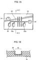
- Figure 1A is a schematic plane view of a device substrate
- Figure 1B is a cross sectional view of the device shown in Figure 1A in the I-I direction.
- Both drawings illustrating a microchip are schematic views provided only for the purpose of describing the present invention in a simpler way, and the dimension and shape therein do not reflect those of an actual microchip.
- the device substrate includes a substrate 10 compatible with the liquids, and substrate 10 comprises sample inlet unit 31, solvent unit 32, reagent units 33a and 33b, dent serving as a wastewater reservoir 34, and flow channels (grooves) 40 for connecting the respective dents.
- monolayers 20 non-compatible with the liquid are formed on the internal surface of flow channel 40 along the traveling direction of the liquid. More specifically, the monolayers 20 are formed all over the internal surface of the groove except parts of the bottom and side faces thereof and the areas whereon no monolayer 20 is formed are areas compatible with the liquid.
- substrates having active hydrogen on the substrate surface in flow channels are preferably used as the compatible substrate.
- the width of the compatible area varies according to the kind of flowing liquid, but is preferably 0.5 ⁇ m or more and more preferably 1 ⁇ m or more. On the other hand considering the ratio of compatible to non-compatible areas, the width is preferably 10 ⁇ m or less and more preferably 5 ⁇ m or less.
- non-compatible areas at some parts of continuous flow channels and compatible areas at the other part thereof, it is also possible to change the flow rate of liquids flowing through the flow channels locally, as the liquids flow more rapidly than in compatible areas due to the decrease in the wettability of the liquids flowing through the flow channels in the non-compatible areas.
- the present invention advantageously provides a device substrate whereon various flow channels different in the flow characteristics of liquids can be formed on the device substrate described above.
- the dimension of the entire device substrate is not particularly limited, but usually 5 to 100 mm in length, 5 to 100 mm in width, and 500 to 5,000 ⁇ m in thickness.
- the width of the flow channels on the substrate is not particularly limited, but usually 10 ⁇ m or more and more preferably 50 ⁇ m or more. On the other hand the width is preferably 300 ⁇ m or less and more preferably 100 ⁇ m or less for miniaturization of the substrate.
- the depth of the flow channels is preferably 10 ⁇ m or more and 100 ⁇ m or less, and more preferably 30 ⁇ m or more and 50 ⁇ m or less, for the same reason. Further, the ratio (area %) of the compatible areas in the entire internal surface of the flow channels is, for example, in the range of about 0.1 to 1%.
- the monolayer may be a single layer or laminated layers consisting of several monolayers.
- the thickness of the monolayer is, for example, in the range of 0.5 to 2 nm; the thickness of the laminated layers may vary according to the number of layers, but is, for example, in the range of 1 to 100 nm, preferably in the range of 1 to 10 nm, and more preferably in the range of 1 to 6 nm; and the number of layers is, for example, in the range of 2 to 100, preferably in the range of 2 to 50, and particularly preferably in the range of 2 to 6.
- Examples of the substrates for use in the present invention are substrates hitherto known in the art including glass substrates, quartz substrates, synthetic quartz substrates, silicon substrates, various polymer substrates such as acrylic substrate, polystyrene substrate, polyvinyl chloride substrate, epoxy resin substrate, silicone resin (polydimethylsilicone) substrate, PMMA (polymethyl methacrylate) substrate, and polycarbonate substrate; ceramic substrates; metal substrates; and the like.
- glass and quartz substrates are preferable, as they have a structure having many hydroxyl groups on the surface thereof.
- the substrates for microchips include those having another substrate adhered or bonded to the substrate described above.
- the substrate having in the internal surfaces of flow channels the areas non-compatible with the liquid flowing through the flow channels is prepared by coating the monolayer non-compatible with the liquid on the surface of the substrate having particular grooves.
- the areas having the active hydrogens may be only on the substrate surface in flow channels whereon the monolayer is desirably formed.
- the monolayer is preferably prepared in the monolayer-forming process of providing as the organic molecule an organic molecule having a functional group capable of forming a covalent bond in reaction with the active hydrogen on the substrate surface at one end of the molecular chain and a characteristic group non-compatible with the liquid to be placed at the other end, bringing the organic molecule into contact with the substrate, and thus progressing a condensation reaction.
- the portion of organic compound other than the active hydrogen may be present on the substrate.
- the portion of organic compound other than the active hydrogen may be present inside the substrate, and the portion of organic compound other than the active hydrogen may bind to the constituent elements of the substrate. More specifically, if a substrate has, for example, a metal oxide as the constituent material and the group having an active hydrogen is -PO 3 H, all of the -PO 3 H group may be exposed or only -OH group of the -PO 3 H group may be exposed.
- the -PO 2 - portions hidden in the substrate may be -PO 2 - per se, or the oxygen bound to P may bind, for example, to a metal atom (metal ion) M 1 in bulk metal oxide, forming a structure of -P-O-M 1 -.
- a metal atom metal ion
- the substrate should have active hydrogens only when a monolayer is formed, and thus may have previously a sufficient amount of active hydrogens for forming a monolayer or the substrate surface in the flow channel may be granted with the active hydrogens before the monolayer-forming process.
- the covalent bond formed by the condensation reaction of the active hydrogen with the terminal functional group of an organic molecule described below is at least one covalent bond selected from the group consisting of M-O, M-N and M-S bonds (M: Si, Ti, Al or Sn), depending on the structure of the characteristic group having the active hydrogen present on the substrate and the kind of the organic molecule, i.e., the raw material for monolayer.
- the bond preferably is preferably a bond containing at least one structure selected from the group consisting of Si-O, Si-N, and Si-S bonds, more preferably a Si-O or Si-N bond, and still more preferably a Si-O bond, from the viewpoint of easier manufacture.
- the organic molecule forming the monolayer has a terminal functional group capable of forming a covalent bond with the substrate surface above at a terminal thereof and a characteristic group non-compatible with the liquid at the other terminal.
- the characteristic group "non-compatible with the liquid” may be selected suitably according to the kind of liquid used, but is preferably, for example, hydrophobic if the solution is aqueous as in the case where the substrate is used as an integrated microchip.
- the terminal group is one of the terminal groups.
- the degree of hydrophobicity is determined relatively according to the liquid to be placed.
- the critical surface energy of the substrate surface is preferably 25 mN/m or less and more preferably 8 mN/m or more at 20°C.
- the critical surface energy is obtained by measuring contact angles by using standard solutions for measuring critical surface energy and a static contact-angle meter, and is a value determined by plotting the energy values of the standard solutions against the values of cosine contact angles, and extrapolating the line to the energy value at a cosine value of 0.
- the difference in critical surface energy between the hydrophilic and hydrophobic portions when the liquid is an aqueous solution may be selected properly according to the area whereon the monolayer is formed and the aqueous solution used, but is preferably 20 mN/m or more and more preferably 40 mN/m or more.
- the aforementioned difference is preferably 75 mN/m or less and more preferably 65 mN/m or less.
- the degree of hydrophobicity is such that when a droplet of 5.3 ⁇ L is dropped on the surface of a monolayer at 20°C, the contact angle between the droplet and the surface is preferably 80 to 180°, more preferably 90 to 180°, and still more preferably 100 to 160°.
- the contact angle may be determined, for example, according to the measuring method specified in JIS R3257: 1999.
- the organic molecule used for forming the hydrophobic monolayer according to the present invention is preferably a molecule having one of the structures represented by the following Formulae (i) to (iii).
- the halogen atom in the trihalogenated silyl groups is F, Cl, Br, or I.
- chlorosilyl group is preferable.
- the alkoxy group in the trialkoxy silyl group above is particularly preferably a group having 1 to 3 carbons. Specific examples thereof include methoxysilyl, ethoxysilyl, and butoxysilyl groups.
- Organic silane compounds having one of the many substituted silyl groups at one of the terminals form a covalent bond with the substrate as described above, and the monolayers formed are more tightly bound to the substrate.
- an organic molecule is covalently bound to the substrate via a siloxane bond (-Si-O-), by a dehydrohalogenation reaction if the organic molecule is a halogenated silyl group; by a dealcoholization reaction if an alkoxy silyl group; or by an isocyanate-removing reaction if an isocyanate silyl group.
- the covalent bond formed between the organic molecule and the substrate varies according to the kind of the group having an active hydrogen on the substrate surface, and when the group having an active hydrogen is, for example, an -NH group, -SiN bond is formed as the covalent bond.
- the terminal bonding functional group is a multiply substituted silyl group
- the silyl group forms covalent bonds at two sites or more, by forming covalent bonds by condensation reaction with the active hydrogen of the substrate not only at one substituent but also at the other substituents as shown in the following General Formula (6). If there are not a sufficient amount of bond-forming active hydrogens on the substrate surface, neighboring organic molecules may bind to each other.
- Q is at least one atom selected from O, N and S; and the Si is covalently bound via each element to the substrate or a neighboring organic silane group.
- the bivalent characteristic group of General Formula (2) or the trivalent characteristic group of General Formula (5) preferably has a main chain having a total carbon number of 8 or more and 22 or less and preferably 8 or more and 18 or less, especially if the substrate is to be used in analytical instruments for analyzing biomacromolecules.
- the main chain means a longer chain having the greatest number of carbons if there is a branched chain in the molecule.
- C 2 H 4 O group is preferable as the cyclic ether group having 2 to 4 carbons. If the organic compound has a C 2 H 4 O group, the thickness of monolayer can be increased easily by using the ring-opening (addition) reaction of the epoxy groups. A sufficient uniformity in layer thickness can also be achieved easily at the same time.
- the organic compound has a C 2 H 4 O group at the terminal end not forming a covalent bond
- it is possible to expand the thickness of the monolayer by bringing an alcohol additionally to the monolayer formed, allowing the ring-opening (addition) reaction of the epoxy group to proceed, and thus connecting the portion of the alcohol other than -OH (hydrocarbon group) thereto.
- CF 3 -, CH 2 Br-, and CH 2 Cl- are preferable, and CF 3 - is more preferable as the halogen-substituted methyl group, for obtaining a sufficiently hydrophobic monolayer more reliably.
- Organic molecules having CF 3 - as the terminal characteristic group are more easily oriented, raising the molecular density of organic compounds when they are aligned on the substrate while the monolayers are formed. Therefore, hydrophobic monolayers can be prepared more reliably.
- the organic molecule having a structure represented by (i) is preferably at least one organic molecule selected from the group consisting of the compounds represented by the following General Formulae (20) to (29) and the derivatives thereof.
- M, Z 1 , Z 2 , and a are the same as those in General Formula (1) of organic molecule (i) above.
- q is an integer of 2 to 22.
- m and n each are an integer satisfying at the same time the conditions shown in the following Formulae (I) to (III): 0 ⁇ m ⁇ 14... (I); 0 ⁇ n ⁇ 15... (II); and 2 ⁇ (m+n) ⁇ 22... (III).
- the organic molecule having a structure of (ii) is preferably at least one organic molecule selected from the group consisting of the compounds represented by the following General Formulae (30) to (39) and the derivatives thereof.
- Z 1 , Z 2 and a are the same as those in General Formula (1) of organic molecule (i) above.
- A represents at least one bivalent characteristic group selected from the group consisting of the characteristic groups represented by General Formula (3), -O-, -COO-, -C 6 H 4 -and the derivatives thereof.
- t is an integer of 1 to 10.
- p is an integer of 1 to 18.
- r and s each are an integer satisfying at the same time the conditions shown by the following Formulae (IV) to (VI): 0 ⁇ r ⁇ 14... (IV); 0 ⁇ s ⁇ 15... (V); and 2 ⁇ (r+s) ⁇ 22... (VI).
- the organic molecule having the structure of (iii) is preferably at least one organic molecule selected from the group consisting of the compounds represented by the following General Formulae (40) to (49) and the derivatives thereof.
- M, Z 1 , Z 2 and a are the same as those in General Formula (1) of organic molecule (i) above.
- t is an integer of 1 to 10.
- p is an integer of 1 to 18.
- r and s each are an integer satisfying at the same time the conditions shown by the following Formulae (IV) to (VI): 0 ⁇ r ⁇ 14... (IV); 0 ⁇ s ⁇ 15... (V); and 2 ⁇ (r+s) ⁇ 22... (VI).
- organic molecules represented by General Formulae (20) to (29) are preferable, from the viewpoints of ensuring the uniformity of monolayer and the molecular density of organic compounds aligned on the particular area when the monolayer is formed.
- the organic molecules represented by the following Formulae (201) to (203) are preferable: CF 3 (CF 2 ) 7 (CH 2 ) 2 SiCl 3 CF 3 (CF 2 ) 7 (CH 2 ) 2 Al(OCH 3 ) 3 CF 3 (CF 2 ) 7 (CH 2 ) 2 TiCl(CH 3 ) 2
- the organic molecules represented by General Formula (21) are preferable: CH 3 (CH 2 ) 7 (CH 2 ) 2 SiCl 3 CH 3 (CH 2 ) 7 AlCl(OC 2 H 5 ) 2 CH 3 (CH 2 ) 7 TiCl(C 3 H 7 ) 2 CH 3 (CH 2 ) 4 SnCl(C 3 H 7 ) 2
- organic molecules represented by General Formulae (30) to (39) are preferable, from the viewpoints of ensuring the uniformity of monolayer and the molecular density of organic compounds aligned on the particular area when the monolayer is formed.
- the organic molecules represented by the following Formulae (301) to (306) are preferable: CF 3 (CF 2 ) 3 (CH 2 ) 2 O(CH 2 ) 15 SiCl 3 CF 3 COO(CH 2 ) 15 SiCl 3 CF 3 (CF 2 ) 3 (CH 2 ) 2 Si(CH 3 ) 2 (CH 2 ) 9 SiCl 3 CF 3 (CF 2 ) 7 Si(CH 3 ) 2 (CH 2 ) 9 SiCl 3 CF 3 (CH 2 ) 2 Si(CH 3 ) 2 (CH 2 ) 15 SiCl 3 CF 3 CH 2 O(CH 2 ) 15 SiCl 3
- the organic molecules represented by the following Formulae (307) to (312) are preferable: CH 3 (CH 2 ) 3 (CH 2 ) 2 O(CH 2 ) 15 SiCl 3 CH 3 COO(CH 2 ) 15 SiCl 3 CH 3 (CH 2 ) 3 (CH 2 ) 2 Si(CH 3 ) 2 (CH 2 ) 9 SiCl 3 CH 3 (CH 2 ) 7 Si(CH 3 ) 2 (CH 2 ) 9 SiCl 3 CH 3 (CH 2 ) 2 Si(CH 3 ) 2 (CH 2 ) 15 SiCl 3 CH 3 CH 2 O(CH 2 ) 15 SiCl 3
- the organic molecule represented by Formula (201) is most preferable.
- organic molecules other than those described above organic molecules described in Jpn. Unexamined Patent Publication Nos. 4-13267, 4-236466, 10-180179, and 4-359031 may be used in the range that provides the advantageous effects of the invention, the contents of which are hereby incorporated by reference.
- reagents include, for example, decyltrichlorosilane manufactured by Sigma-Aldrich, Inc and the like.
- Typical examples of the production methods include the methods described in Jpn. Unexamined Patent Publication Nos. 2-138286 and 4-120082, the contents of which are hereby incorporated by reference.
- the hydrosilylation reaction is preferably carried out in the presence of a platinum catalyst.
- the terminal perfluoroalkyl halogen compounds represented by General Formula (20a) are commercially available short chain compounds and include, for example, F(CF 2 ) 2 CH 2 Cl, F(CF 2 ) 2 CH 2 I, F(CF 2 ) 3 I, and F(CF 2 ) 3 CH 2 Br.
- the hydrogen silanes represented by General Formula (20e) include, for example, HSiCl 3 , HSi(CH 3 )Cl 2 , HSi(CH 3 ) 2 Cl, HSi(OMe) 3 , and HSiCH 3 (OC 2 H 5 ) 2 .
- the Grignard reagents represented by General Formula (20c) are prepared, for example, by first placing magnesium metal in a reaction solvent such as diethylether, tetrahydrofuran, or the like, and then supplying a terminal alkenyl halogenated compound of General Formula (20b) into the solution, for example, at 50 to 60°C.
- the amount of magnesium metal is preferably equimolar to or slightly higher than that of the terminal alkenyl halogenated compound.
- the terminal perfluoroalkene compound of General Formula (20d) is prepared by reacting the Grignard reagent of General Formula (20c) prepared with a terminal perfluoroalkyl halogen compound of General Formula (20a) at room temperature in Grignard reaction.
- the aforementioned Grignard reagent is gradually added into a reaction solvent such as diethylether, tetrahydrofuran, or the like containing the terminal perfluoroalkyl halogen compound of General Formula (20a).
- the terminal perfluoroalkyl halogen compound may be added into a reaction solvent containing the Grignard reagent.
- Cu may also be added as a catalyst.
- the terminal perfluoroalkene compound of General Formula (20d) is obtained after low-boiling compounds such as the reaction solvent and others are removed from the organic phase. If possible, the terminal perfluoroalkene compound may be purified by distillation.
- the desired terminal perfluoroalkyl silane compound is obtained by reacting the terminal perfluoroalkene compound of General Formula (20d) and the hydrogen silane of General Formula (20e), for example, at about 100°C in hydrosilylation reaction.
- organic silane compound represented by General Formula (30) is typically prepared, for example, in the following process:
- Silane compounds represented by General Formula (30a) include, for example, CF 3 (CH 2 ) 2 (CH 3 ) 2 SiCl and CF 3 (CH 2 ) 2 (CH 3 ) 2 SiOCH 3 .
- the hydrosilylation reaction may be carried out at a reaction temperature of 50 to 150°C in the presence of a catalyst, under reflux if the reaction is an atmospheric reaction, or in a state sealed in an autoclave if it is a pressurized reaction, by reacting the equimolar amounts of a terminal perfluoroalkene compound and a silicon compound, or by reacting the terminal perfluoroalkene compound with an excessive amount of the silicon compound as needed for completion of the reaction, as terminal perfluoroalkene compounds are generally expensive.
- an inactive hydrocarbon solvent such as n-hexane, isooctane, toluene, xylene, or the like may be used as needed in the reaction.
- the product is sufficiently pure and usable when the low-boiling compounds including unreacted compounds, reaction solvents, and the like are stripped off after reaction, but may be further purified by distillation if the product is distillable.
- a substrate inherently having a characteristic group with active hydrogen may be used. Also, if the substrate does not have a sufficient amount of active hydrogens, a substrate of which the surface is provided before use with active hydrogens by surface treatment may be used. In particular, if a dense monolayer is desirably formed, the following surface treatment is preferable.
- Methods of providing the substrate with active hydrogens include, for example, methods of oxidizing the surface chemically, treating with plasma in the presence of oxygen, and treating with ozone.
- the methods also include the method of hydrophilizing the substrate, for example, with SiCl 4 , HSiCl 3 , SiCl 3 O-(SiCl 2 -O) ⁇ -SiCl 3 (wherein, ⁇ is an integer of 0 to 6), Si(OH) 4 , HSi(OH) 3 , Si(OH) 3 O-(Si(OH) 2 -O) ⁇ -Si(OH) 3 (wherein, ⁇ is an integer of 0 to 6), or the like.
- the method of oxidizing the surface will be described in more detail.
- the oxidation treatment may be performed, for example, by high-energy irradiation of the surface in the presence of oxygen and a hydrogen atom-supplying substance.
- oxygen in air is decomposed by ultraviolet ray irradiation generating ozone, which in turn reacts with the hydrogen atom-supplying substance and generates active species having an active hydrogen.
- ultraviolet ray irradiation generating ozone which in turn reacts with the hydrogen atom-supplying substance and generates active species having an active hydrogen.
- Substrates having active hydrogens are obtained by the reaction of the unbonded radicals with active species containing active hydrogens.
- Water, ammonia, or the like, for example, is favorably used as the hydrogen atom-supplying substance, from the viewpoints of availability and convenience in handling. If water is used as the hydrogen atom-supplying substance, characteristic groups at least containing the structure represented by -OH are formed. Alternatively, if ammonia is used, characteristic groups at least containing the structure represented by -NH are formed. Corona discharge, oxygen plasma, or other treatment may be used, replacing the ultraviolet-ray irradiation treatment.
- the monolayer non-compatible with liquid is formed on the substrate surface in flow channels in the monolayer-forming process, i.e., by preparing the substrate obtained as described above and coating a certain area therewith on the substrate surface in the flow channel.
- the non-compatible monolayer may be formed, for example, over the entire internal surface of the flow channel in substrate as described as an embodiment of the invention.
- the methods of producing the monolayer are not particularly limited to the methods below, and include those disclosed, for example, in Jpn. Unexamined Patent Publication Nos. 4-13267, 4-236466, and 10-180179, and others, the contents of which are hereby incorporated by reference.
- the monolayer can be formed by bringing the organic molecule above into contact with the substrates having active hydrogens in the manner described above.
- the contact treatment may be carried out either in a gas or liquid phase, liquid phase treatment is preferred because of simplicity in manufacture.
- the substrate is brought into contact with an organic molecule-containing solution, which is prepared by dissolving or suspending the organic molecule in a solvent.
- the solvent is preferably an aprotic solvent, and the moisture in the gas phase in contact with the organic molecule-containing solution is preferably controlled to a relative humidity of 35% or less, as expressed as a relative humidity at 22°C.
- moisture in the gas phase is preferably 25% or less, more preferably 5% or less, as expressed as a relative humidity at 22°C
- the reaction container for use in the process is preferably a sealed system such as a glove box or the like.
- the constituent gas of the gas phase of which the moisture is controlled in the range above is preferably at least one gas selected from the group consisting of noble gases and nitrogen gas.
- air may be used under a condition that sufficiently suppresses oxidation of the organic molecule or aprotic solvent and oxidative degradation of the monolayer.
- air may be used by properly adjusting the temperature of the gas phase and the organic molecule-containing solution, the concentration of organic molecule, the contact time between the organic molecule and the substrate, and the like in the monolayer-forming process.
- an organic molecule-containing solution is first prepared by dissolving the organic molecule in a solvent.
- the aprotic solvent for use in preparing the organic molecule-containing solution may be selected arbitrarily according to the kind of the organic molecule, but is preferably a solvent that dissolves the organic molecule significantly, from the viewpoint of ensuring easy and reliable production of monolayers thinner in thickness (0.5 to 50 nm) and excellent in the uniformity of layer thickness.
- examples thereof include organic solvents such as hexadecane, chloroform, carbon tetrachloride, silicone oil, hexane, toluene, and the like. These solvents may be used alone or in combination of two or more solvents.
- mixed solvents containing hexadecane, chloroform and carbon tetrachloride are preferable as the aprotic solvent.
- Use of the organic solvent in this manner prevents sufficiently, for example, polymerization of the organic molecule caused by the presence of water.
- the use of the organic solvent facilitates the condensation reaction between the terminal bonding functional group of organic molecule and the active hydrogens of substrate.
- the concentration of the organic molecule-containing solution is preferably 10 -4 mol/L or more, more preferably 10 -3 mol/L or more, and most preferably 10 -1 mol/L or less.
- the contact time of the substrate with the organic molecule-containing solution is not particularly limited, but, for example, several seconds to 10 hours and preferably 1 minute to 1 hour.
- the temperature of the organic molecule-containing solution is, for example, 10 to 80°C and preferably in the range of 20 to 30°C.
- the organic molecules are bound to the substrate via covalent bonds [for example, siloxane bond (-Si-O-)], giving a monolayer.
- the monolayer formed in this manner has characteristic groups non-compatible with the liquids described above on the surface, and thus the area on the device substrate according to the present invention where the monolayer is formed, i.e., the entire area of the flow channel, becomes non-compatible with the liquid.
- the methods of forming the monolayer selectively on the substrate surface in the flow channel are not particularly limited and include, for example, the methods described below.
- the chemical absorbent solution, the processing condition, and the like used below are the same as those above, except otherwise specified.
- the first method is a method of forming a monolayer over the entire substrate surface in flow channels and then removing only the monolayer formed in the area whereon the monolayer is not needed, i.e., the compatible area.
- a photomask is additionally formed on the areas to be compatible with liquids of the monolayer (i.e., area wherein the monolayer is not needed).
- the monolayer on the area not covered by the photomask can be removed by irradiating with high-energy ray, for example, ultraviolet ray.
- high-energy ray for example, ultraviolet ray.
- a laser such as an excimer laser or the like is used as the means for the ultraviolet ray irradiation, the ultraviolet ray may be spotted onto particular areas of the monolayer.
- UV-ray irradiation treatment In addition to the ultraviolet-ray irradiation treatment, other method such as corona, plasma, or other treatment may be employed. By conducting these treatments in the presence of oxygen, the monolayer on the substrate surface may be removed by oxidation.
- a monolayer is selectively formed on a substrate surface by forming a resist pattern that covers only the compatible area in the substrate surface in flow channels, bringing the organic molecule described above into contact with the substrate surface whereon the resist pattern is formed, and removing the resist pattern.
- a resist pattern for covering the compatible area is formed.
- the resist pattern can be formed easily by a semiconductor film-producing technology.
- a monolayer is selectively coated on the area not covered by the resist, by bringing an organic molecule to the substrate whereon the resist pattern is formed, and then the resist pattern is removed, to form non-compatible areas.
- the resist pattern may be a positive or negative resist pattern.
- an organic molecule-containing solution is prepared by dissolving the organic molecule in an aprotic solvent. Then, the organic molecule-containing solution and the substrate after the resist pattern is formed are placed in a container such as a glove box or the like, of which the internal moisture in gas phase can be easily controlled in the range described above, to allow a condensation reaction to progress.
- the aprotic solvent used for preparation of the organic molecule-containing solution may be arbitrarily selected according to the kind of the organic molecule, if it is a solvent that does not dissolve the resist pattern, but is preferably a fluorine-based solvent, from the viewpoint of obtaining a monolayer thinner in thickness (0.5 to 50 nm) and superior in the uniformity of layer thickness more easily and reliably.
- the preferable fluorine-based solvents include perfluorocarbon- and hydrofluoroether-derived liquids manufactured by Sumitomo 3M Limited.
- the solvent is preferably "HFE-7200”, “PF-5080”, or “FC-77” (trade name, manufactured by Sumitomo 3M Limited), from the viewpoints of various physical properties of the solvent such as the boiling point suitable for the temperature condition of the processing.
- Reaction conditions such as the concentration and the reaction time of the organic molecule may be similar to those described above.
- the resist pattern can be removed by using, for example, acetone.
- a monolayer is formed selectively by bringing an organic molecule into contact only with the non-compatible area by ink-jet, stamping, or other method.
- the monolayer may be a single layer or a laminated layer having multiple layers.
- the second monolayer may be formed thereon. In such a case, if there are no reactive functional groups on the surface of the first monolayer, active hydrogens may be provided by the surface treatment described above.
- a terminal group not binding to a covalent bond of the first monolayer is a characteristic group containing a group having an unsaturated bond such as a vinyl group or the like
- a characteristic group having at least the structure of -OH can be introduced by irradiating an energy beam such as electron beam, X ray, or the like onto the surface of monolayer under an environment containing moisture and thus changing part of the unsaturated bond-containing group.
- a characteristic group having a an unsaturated bond-containing group such as a vinyl group or the like is bound to the substrate, a characteristic group having at least the structure of -COOH can be introduced, for example, by immersing the substrate in an aqueous potassium permanganate solution and thus changing the structure of part of the unsaturated bond-containing group.
- the thickness of the monolayer may be arbitrarily selected according to the kind (length) of organic molecule or by forming the laminated layer above; or adjusted, for example, by the method of binding additionally a non-compatible molecule to the terminal of the terminal characteristic group of the organic molecule constituting the monolayer after forming the first monolayer.
- the monolayer may be additionally brought into contact, for example, with a Grignard reagent (RMgX) after it is formed.
- a Grignard reagent RMgX
- the contact results in an addition reaction between the terminal characteristic group and RMgX, resulting in connection of the hydrocarbon group (R-) in RMgX to the terminal of the terminal characteristic group.
- R is an alkyl group, halogenated alkyl group, alkenyl group, or halogenated alkenyl group having 1 to 23 carbons
- X is a halogen (F, Cl, Br, or I).
- the monolayer may be additionally brought into contact with an alcohol (ROH) after it is formed.
- R is an alkyl group, halogenated alkyl group, alkenyl group, or halogenated alkenyl group having 1 to 23 carbons
- X is a halogen (F, Cl, Br, or I).
- a desirable device substrate is obtained after the monolayer is formed in the manner described above. If the liquid is an aqueous solution and the hydrophilicity is not satisfactory or desirably increased, the hydrophilicity may be enhanced, for example, by repeating the surface treatment selectively on the areas in flow channels.
- a hydrophilic monolayer is formed on the interior of the flow channels for the hydrophilic surface treatment.
- a hydrophilic monolayer may be formed inside the flow channel on the substrate.
- the hydrophilic monolayer further increases the difference in hydrophilicity between the hydrophilic areas and the hydrophobic monolayer areas formed surrounding them.
- (A) an organic molecule having a terminal functional group capable of forming a covalent bond with a substrate and other terminal group hydrophile with a liquid, or (B) an organic molecule having a terminal functional group capable of forming a covalent bond with a substrate and other terminal group which can be modified to a hydrophilic group after the monolayer may be used.
- Examples of the organic molecules (A) in the former group, which have a hydrophilic terminal group include organic molecules represented by the following General Formula (50).
- T 1 represents a CHO group, COOH group, OH group, NH 2 group, COOR group, PO(OH) 2 group, PO(OH) group, SO 3 H group, SO 2 H group or SH group;
- ⁇ is a number required for making the total molecular length of the compound including the terminal functional group above shorter than or as small as the molecular length of the organic group that forms hydrophobic monolayer;
- Z 4 represents an alkoxy groups having 1 to 5 carbons;
- Z 5 represents at least one atom or atomic group selected from the group consisting of H and alkyl groups having 1 to 5 carbons; and
- ⁇ is an integer of 1 to 3.
- the organic molecules include those wherein the terminal group not forming a covalent bond with the substrate surface is substituted with a group having an active hydrogen such as a hydroxyl, amino, or other group. These organic molecules are immobilized tightly on the substrate by forming a covalent bond when they are brought into contact with the substrate. Because the terminal group opposite to the covalent bond is a hydrophilic group, the liquids flowing in flow channels become in contact only with the areas where the hydrophilic monolayer is formed.
- Organic molecules having a hydrophilic terminal group include the following compounds (501) to (508): H 2 N(CH 2 ) 3 Si(OCH 3 ) 3 OHC(CH 2 ) 3 Si(OCH 2 CH 3 ) 3 HOOC(CH 2 ) 5 Si(OCH 3 ) 3 HO(CH 2 ) 5 Si(OCH 3 ) 3 H 3 COOC(CH 2 ) 5 Si(OCH 2 CH 3 ) 3 (OH) 2 OP(CH 2 ) 3 Si(OCH 3 ) 3 HO 2 S(CH 2 ) 3 Si(OCH 3 ) 3 HS(CH 2 ) 3 Si(OCH 3 ) 3
- the latter organic molecules (B) of providing a monolayer withhydrophilicity is a method of substituting the terminal group of a compound that is hydrophobic when prepared with a hydrophilic group by the aforementioned monolayer-forming process.
- a hydroxyl group (-OH) may be introduced to an organic molecule having a double bond at the terminal, by irradiating the molecule with a high-energy beam such as electron beam, X ray, or the like under an environment containing moisture.
- a carbonyl group for example, by immersing the substrate in an aqueous potassium permanganate solution.
- the compound has, for example, a cyano group (-CN group)
- the cyano group may be converted to an amino group by reducing it in a lithium aluminum hydride solution.
- the ring-opening reaction of an epoxy group may also be used.
- Such organic molecules include those represented by the following General Formula (60): T 2 -(C v H 2v )-Si-(Z 6 ) ⁇ (Z 7 ) 3- ⁇ [wherein, T 2 represents a vinyl, methyl, halogenated methyl, epoxy, or cyano group; v is a number required for making the total molecular length of the compound including the terminal functional group above shorter than or as short as the molecular length of the organic group that forms hydrophobic monolayer; Z 6 represents at least one atom or atomic group selected from the group consisting of F, Cl, Br, I, -OH, -SCN, -NCO, and alkoxy groups having 1 to 5 carbons; Z 7 represents at least one atom or atomic group selected from the group consisting of H and alkyl groups having 1 to 5 carbons; and p is an integer of 1 to 3.]
- T 2 represents a vinyl, methyl, halogenated methyl, epoxy, or cyano group
- v is a number required for
- Covalent bonds are formed and thus a monolayer is formed by bringing the organic molecule having the terminal group above into contact with the substrate.
- the terminal group is a double bond
- the terminal double bond can be converted into a hydrophilic carboxyl group by bringing the compound into contact with an aqueous potassium permanganate solution.
- the total carbon number of the characteristic group of the organic compound above present between the terminal bonding functional group capable of forming a covalent bond and the hydrophilic terminal group is properly determined so that the molecular length of the organic molecule becomes shorter than that of the non-compatible monolayer surrounding the area where the organic molecule is coated as a monolayer.
- the degree of hydrophilicity is determined relative to the surrounding hydrophobic monolayer, and thus the hydrophilic monolayer should only have a greater critical surface energy than that of the hydrophobic monolayer.
- the critical surface energy thereof is preferably more than 20 mN/m, more preferably 60 mN/m or more, and more preferably 75 mN/m or less.
- the hydrophilic monolayer may be formed after a hydrophobic monolayer is formed or in advance to formation of a hydrophobic monolayer.
- a monolayer of the present invention may be changed the compatibility with a liquid
- the particular area of the flow channel can be coated with a monolayer non-compatible with the liquid, i.e., with the monolayer above according to the present invention, properly according to the liquid to be placed. Therefore, even if the liquid to be placed is not an aqueous solution, the present invention may be used in an analogous manner for confining the liquid in particular areas by using the difference in affinity to the liquid.
- the substrates made only of the device substrate according to the present invention may be applied to microchips.
- Substrates in the structure having compatible areas in flow channels may be used in such applications.
- the substrate according to the present invention may be in the structure wherein it is adhered to another substrate.
- a microchip is prepared by using the device substrate having flow channels according to the present invention as the bottom substrate and conjugating a top substrate thereto.
- a substrate having a non-compatible monolayer is favorable used as the top substrate.
- another substrate may be placed atop the substrate via a spacer or the like, in the manner that it faces the substrate described above.
- the other substrate atop preferably has through-holes, for example, for addition of samples, reagents, and the like, and for degasification.
- the bottom substrate has reagent-storing, reaction, measurement, and other units, and flow channels are connected to respective units.
- Substrate, enzyme, reaction-terminating, and other solutions are injected through the through-holes previously placed in the top substrate into the respective units.
- the internal surface of respective storing units is preferably coated with a monolayer non-compatible with the liquids to be placed as well.
- the transportation of respective solutions and the reaction solutions are controlled by a micropump or the like, and the reagents fed into a predetermined reaction unit react therein.
- the reaction time in this reaction unit is properly determined and the reaction is discontinued by injection of a reaction-terminating solution after a particular period of time.
- the reaction solution is fed via a flow channel into a measurement unit for measurement by a spectroscopic method or the like.
- the device substrate according to the present invention may be used for the method of analyzing samples that requires adjustment of the flow rate of liquids by modifying the monolayer, and the flow rate of the liquids may be changed by properly selecting the area and shape of the monolayer in the internal surface of flow channels and the kind of the monolayer. Further, if the monolayer coating the internal surface of flow channels is formed by two or more kinds of monolayers different in compatibility with the liquids, it becomes possible to change the flow rate of the liquids by modifying the difference in compatibility.
- the microchip above may be used in microchip modules in combination with the detection means known in the art.
- Microchips are produced as follows:
- a glass substrate (length: 76 mm, width: 26 mm, and thickness: 2 mm) having units for storing a substrate solution, enzyme solution, and reaction-terminating solution, reaction unit, and measurement unit was prepared as a bottom substrate.
- Flow channels are connected to respective units (substrate-storing unit, enzyme-storing unit, reaction-terminating solution-storing unit); a reaction unit is placed at the intersection of the flow channels; and another flow channel is additionally connected to the reaction unit.
- the flow channel connected to the reaction unit is further connected at the other end to a measurement unit, to which yet another flow channel is connected, which in turn is connected to a discharge outlet.
- the outlet is connected to an external tube for discharge.
- the flow channels above are in the shape of groove having a width of 100 ⁇ m and a depth of 30 ⁇ m, and the respective storing units and the reaction unit are columnar dents having a diameter of 3 mm and a depth of 30 ⁇ m.
- the glass substrate was washed with pure water and air-dried, then washed with ethanol and air-dried, and washed with ultraviolet-ray and ozone.
- the resulting glass substrate was stored in a glove box to which nitrogen gas having a dew point of -55°C is supplied.
- the glass substrate was brought into contact with the trichlorosilane compound described above, as the glass substrate was immersed in a 1.0 weight % non-aqueous solution containing F(CF 2 ) 8 (CH 2 ) 2 SiCl 3 (hydrofluoroether; trade name: HFE7100; manufactured by Sumitomo 3M Limited) at room temperature.
- a glass substrate (length: 76 mm, width: 26 mm, and thickness: 1 mm) was made available as the cover (top substrate) of the bottom substrate, and a monolayer was formed thereon in a similar manner to the bottom substrate.
- the resulting top substrate was adhered to the bottom substrate with the monolayer-formed surface facing the bottom substrate, to give a microchip.
- a substrate (length: 76 mm, width: 26 mm, and thickness: 2mm) whereon two grooves are formed crosswise was made available, and a monolayer was formed on the substrate surface (including the internal surface of grooves) under a condition similar to that of the EXAMPLE 1.
- the width and the depth of the grooves were both 120 ⁇ m, and the distances between the intersection of the cross and the ends of the grooves were 10 mm.
- a top substrate having a monolayer similar to that of EXAMPLE 1 was placed on the substrate, to give a microchip.
- a glass substrate having units for storing substrate solution, enzyme solution and reaction-terminating solution, a reaction unit, and a measurement unit was prepared in the similar manner to EXAMPLE 1 as a bottom substrate. Used was a substrate whereon flow channels (width 100 ⁇ m, depth 30 ⁇ m) were connected to respective storing units (substrate-storing unit, enzyme-storing unit, reaction-terminating solution-storing unit).
- a monolayer was formed in a similar manner to EXAMPLE 1, except that the glass substrate and the organic molecule-containing solution above were used.
- a photomask was placed on the glass substrate whereon the monolayer was formed, for forming hydrophilic areas on the flow-channel bottom faces.
- Ultraviolet ray (light source: 110-W lamp, manufactured by SEN light Corporation) was irradiated for 8 seconds through the photomask. It was found that a device substrate wherein the substrate is exposed in the flow channels could be produced by adjusting the irradiation width at 1 ⁇ m.
- the flow channels of the glass substrate used in EXAMPLE 3 was coated with a positive resist; the photomask identical with that used in EXAMPLE 3 was placed on the substrate; and a resist pattern was formed thereon via a resist-exposure process, developing process, and cleaning process.
- a hydrophobic monolayer was formed on the entire surface in the flow channels of the substrate in the analogous manner to the preparation of the monolayer of EXAMPLE 3.
- the substrate was irradiated with a pulsed laser (540 nm, femtosecond pulse, output: 13 mW, and laser beam diameter: 1.5 ⁇ m). It was confirmed that it was possible to prepare by laser irradiation a device substrate having hydrophilic areas on the bottom faces of flow channels along the traveling direction of liquids.
- a pulsed laser 540 nm, femtosecond pulse, output: 13 mW, and laser beam diameter: 1.5 ⁇ m.
- the device substrate prepared in EXAMPLE 5 was hydrophilized as follows.
- a solution was pushed away on the monolayer of the substrate and adhered only on the areas where the monolayer above was removed. After the solution was evaporated, the device substrate was treated in hot air at 120°C. By this treatment, a hydrophilic monolayer was coated on the areas on the glass substrate where the monolayer was removed. The areas became hydrophilic by the amino groups provided. The fact that a desired hydrophilic monolayer was formed was confirmed by monitoring the presence or absence of the absorptions corresponding to the CH 2 and NH 2 bonds in the infrared absorption spectrum.
- the device substrate of EXAMPLE 3 whereon a compatible area was formed on the bottom faces of flow channels was used.
- microchips prepared in EXAMPLES 1 and 2 were subjected to the following evaluation tests, respectively together with the microchips for comparison whereon monolayer is not formed.
- microchips prepared in EXAMPLE 1 and a microchip whereon no monolayer is formed were evaluated as follows.
- a substrate solution, an enzyme solution, and a reaction-terminating solution were injected into the respective storing units on each microchip through the through-holes which were previously placed in the top substrate in a similar manner to above. Transfer of the respective solutions and the reaction solution was controlled by a micorpump in a conventional manner.
- ⁇ -Galactosidase was dissolved in the buffer solution, to give enzyme solutions at concentrations of 0.1 and 0.5 mg/mL.
- Ortho-nitrophenylgalactosidase was dissolved in the buffer solution, to prepare a 0.1 mg/ml substrate solution.
- the substrate solution and the enzyme solution were fed into the reaction unit to start the reaction.
- Ortho-nitrophenol was generated by the reaction of the enzyme and the substrate in the reaction unit.
- the reaction-terminating solution was injected from the reaction-terminating solution-storing unit via the flow channel connected to the reaction unit, to discontinue the reaction.
- the reaction solution after discontinuation was transferred via the flow channel leading to the measurement unit, wherein the absorption intensity thereof at a wavelength of 420 nm was determined by using ultraviolet and infrared spectrometer.
- the absorption wavelength of the ortho-nitrophenol is 420 nm.
- the absorbance of the microchip for comparison prepared in a similar manner to EXAMPLE 1 except that both the bottom and top substrates were not coated with the monolayer was determined.
- the microchip of EXAMPLE 1 had an average of the absorbencies in multiple measurements (5 times) after respective reaction times of 0.98 and an error of 0.02 or less, when 0.5 mg/mL enzyme solution was used.
- the microchip for comparison had an average of the absorbencies in multiple measurements (5 times) after respective reaction times of 0.67 and an error of about 0.1, when 0.5 mg/mL enzyme solution was used.
- the microchip of EXAMPLE 1 whereon a monolayer is formed is higher in measurement sensitivity and accuracy than that of COMPARATIVE EXAMPLE 1, even when the same enzyme at the same concentration was used. It is probably because transfer and mixing of the liquids are faster and the adhesion of the enzyme and substrate onto the flow channels are prevented.
- microchips prepared from the substrate of EXAMPLE 2 and the substrate of EXAMPLE 2 having no monolayer formed were evaluated as follows.
- a mixed DNA sample containing various DNA fragments was separated by electrophoresis, by injecting the DNA sample at one end of a groove and applying a voltage (100 V/cm) between one end and the other end of the groove.
- a voltage 100 V/cm
- DNA separation from the mixed DNA solution was confirmed both on the microchips of EXAMPLE 2 and for comparison.
- examination of the separation accuracy by a spectroscopic method revealed that the accuracy of the microchip of EXAMPLE 2 is approximately 4 times higher than that of the microchip for comparison. The result indicates that it is possible to improve the separation accuracy and shorten the processing time only by forming a monolayer, for example, without elongation of the processing time, increase in the number of separation operations, or the like which was considered hitherto necessary.
- the device substrate according to the present invention which has the non-compatible monolayer on the internal surface of flow channels permits faster transfer of the liquids in the flow channels, due to the change in wettability to the liquid caused by the noncompatibility of the monolayer.
- presence of the non-compatible areas on the internal surface of the flow channels prevents adhesion and retention of the liquids on the internal surface caused by the surface tension or the like, enabling faster liquid transfer.
- the prevention of the retention of liquids described above permits effective use of trace amounts of samples.
- the layer on the substrate surface in flow channels is a monolayer having a thickness at the nano order, which cause no problems in visual observation and optical analysis. Further, the substrate and the monolayer are bound to each other via covalent bonds, extremely strong bonds, eliminating the concern about the separation of the monolayer during handling.
- the device substrate according to the present invention allows, for example, miniaturization of circuits and more efficient use of smaller amounts of samples, and thus the device substrate according to the present invention is useful in various areas including medical care, development of new drugs, analysis, and the like as the substrates for the various microchips described above, in particular for integrated microchips.
- a device substrate comprising a substrate having a flow channel of a liquid, wherein an internal surface of said flow channel has an area non-compatible with said liquid; said area non-compatible with the liquid is formed by a monolayer non-compatible with said liquid; and said monolayer is connected to said substrate via a covalent bond, which allows smooth flow of the liquid in the minute flow channel.
Landscapes
- Chemical & Material Sciences (AREA)
- Health & Medical Sciences (AREA)
- Life Sciences & Earth Sciences (AREA)
- Engineering & Computer Science (AREA)
- Chemical Kinetics & Catalysis (AREA)
- Immunology (AREA)
- Organic Chemistry (AREA)
- Materials Engineering (AREA)
- Geochemistry & Mineralogy (AREA)
- Hematology (AREA)
- General Chemical & Material Sciences (AREA)
- Urology & Nephrology (AREA)
- Analytical Chemistry (AREA)
- General Health & Medical Sciences (AREA)
- Molecular Biology (AREA)
- Biomedical Technology (AREA)
- Cell Biology (AREA)
- Biotechnology (AREA)
- Microbiology (AREA)
- Clinical Laboratory Science (AREA)
- Dispersion Chemistry (AREA)
- Food Science & Technology (AREA)
- Medicinal Chemistry (AREA)
- Physics & Mathematics (AREA)
- Biochemistry (AREA)
- General Physics & Mathematics (AREA)
- Pathology (AREA)
- Application Of Or Painting With Fluid Materials (AREA)
- Physical Or Chemical Processes And Apparatus (AREA)
Applications Claiming Priority (2)
| Application Number | Priority Date | Filing Date | Title |
|---|---|---|---|
| JP2003320010 | 2003-09-11 | ||
| JP2003320010 | 2003-09-11 |
Publications (2)
| Publication Number | Publication Date |
|---|---|
| EP1514596A2 true EP1514596A2 (de) | 2005-03-16 |
| EP1514596A3 EP1514596A3 (de) | 2005-09-21 |
Family
ID=34132038
Family Applications (1)
| Application Number | Title | Priority Date | Filing Date |
|---|---|---|---|
| EP04021477A Withdrawn EP1514596A3 (de) | 2003-09-11 | 2004-09-09 | Substrat, Herstellungsverfahren und Mikrochip |
Country Status (2)
| Country | Link |
|---|---|
| US (1) | US20050059139A1 (de) |
| EP (1) | EP1514596A3 (de) |
Cited By (2)
| Publication number | Priority date | Publication date | Assignee | Title |
|---|---|---|---|---|
| US20070224082A1 (en) * | 2005-07-26 | 2007-09-27 | Kazufumi Ogawa | Biochemical chip and production method thereof |
| EP2008715A1 (de) * | 2007-06-25 | 2008-12-31 | ibidi GmbH | Probenkammer |
Family Cites Families (16)
| Publication number | Priority date | Publication date | Assignee | Title |
|---|---|---|---|---|
| JP2907515B2 (ja) * | 1990-09-07 | 1999-06-21 | 松下電器産業株式会社 | 末端パーフルオロアルキルシラン化合物及びその製造方法 |
| JPH0763670B2 (ja) * | 1991-02-06 | 1995-07-12 | 松下電器産業株式会社 | 有機コーティング膜の製造方法 |
| ATE235292T1 (de) * | 1994-10-22 | 2003-04-15 | Central Research Lab Ltd | Verfahren und vorichtung fur diffusionsaustausch zwischen nicht mischbare flüssigkeiten |
| US5904824A (en) * | 1997-03-07 | 1999-05-18 | Beckman Instruments, Inc. | Microfluidic electrophoresis device |
| US6143496A (en) * | 1997-04-17 | 2000-11-07 | Cytonix Corporation | Method of sampling, amplifying and quantifying segment of nucleic acid, polymerase chain reaction assembly having nanoliter-sized sample chambers, and method of filling assembly |
| US6576478B1 (en) * | 1998-07-14 | 2003-06-10 | Zyomyx, Inc. | Microdevices for high-throughput screening of biomolecules |
| US6258454B1 (en) * | 1998-09-01 | 2001-07-10 | Agilent Technologies Inc. | Functionalization of substrate surfaces with silane mixtures |
| EP1314472A1 (de) * | 1998-10-09 | 2003-05-28 | Motorola, Inc. | Integrierte Vielschichtmikrofluidbauteile und Verfahren zu ihrer Herstellung |
| US6555389B1 (en) * | 1999-05-11 | 2003-04-29 | Aclara Biosciences, Inc. | Sample evaporative control |
| US7004184B2 (en) * | 2000-07-24 | 2006-02-28 | The Reagents Of The University Of Michigan | Compositions and methods for liquid metering in microchannels |
| CN1187596C (zh) * | 2000-09-21 | 2005-02-02 | 松下电器产业株式会社 | 扫描探针显微镜,及其探针和制造方法,及使用其的分子加工法 |
| SE0004351D0 (sv) * | 2000-11-27 | 2000-11-27 | Helen Andersson | System och metod för tidstyrd vätskehantering för reaktioner och processer i ett mikrofluidiskt flödescellsystem |
| JP2002236131A (ja) * | 2000-12-08 | 2002-08-23 | Minolta Co Ltd | マイクロチップ |
| US7338760B2 (en) * | 2001-10-26 | 2008-03-04 | Ntu Ventures Private Limited | Sample preparation integrated chip |
| WO2003044519A1 (en) * | 2001-11-20 | 2003-05-30 | Nec Corporation | Separation apparatus, method of separation, and process for producing separation apparatus |
| CN100514065C (zh) * | 2003-08-27 | 2009-07-15 | 松下电器产业株式会社 | 微芯片及其制造方法以及使用微芯片的检查方法 |
-
2004
- 2004-09-08 US US10/935,314 patent/US20050059139A1/en not_active Abandoned
- 2004-09-09 EP EP04021477A patent/EP1514596A3/de not_active Withdrawn
Cited By (5)
| Publication number | Priority date | Publication date | Assignee | Title |
|---|---|---|---|---|
| US20070224082A1 (en) * | 2005-07-26 | 2007-09-27 | Kazufumi Ogawa | Biochemical chip and production method thereof |
| US8252249B2 (en) * | 2005-07-26 | 2012-08-28 | Kazufumi Ogawa | Biochemical chip and production method thereof |
| EP2008715A1 (de) * | 2007-06-25 | 2008-12-31 | ibidi GmbH | Probenkammer |
| EP2263797A1 (de) * | 2007-06-25 | 2010-12-22 | ibidi GmbH | Probenkammer |
| US8001857B2 (en) | 2007-06-25 | 2011-08-23 | Ibidi Gmbh | Sample chamber |
Also Published As
| Publication number | Publication date |
|---|---|
| US20050059139A1 (en) | 2005-03-17 |
| EP1514596A3 (de) | 2005-09-21 |
Similar Documents
| Publication | Publication Date | Title |
|---|---|---|
| KR910000751B1 (ko) | 유기폴리머 막(膜) 표면의 실릴(silyl)화 방법 및 이것을 사용한 패턴(pattern) 형성방법 | |
| US7285674B2 (en) | Silane molecules with pre-activated and protein-resistant functionalities and silane films comprising such molecules | |
| US20020125135A1 (en) | Microfluidic surfaces | |
| EP2442908B1 (de) | Verfahren zur oberflächenbehandlung von mikrofluidischen vorrichtungen | |
| Lee et al. | Controlled silanization: high molecular regularity of functional thiol groups on siloxane coatings | |
| WO2006083600A1 (en) | High aspect ratio performance coatings for biological microfludics | |
| EP3207992B1 (de) | Fotochemische modifizierung einer festen oberfläche | |
| WO2008063134A1 (en) | Method of producing a pattern of discriminative wettability | |
| US20030080087A1 (en) | Process for surface modification of a micro fluid component | |
| US7507675B2 (en) | Device manufacturing method and device | |
| JP4505287B2 (ja) | マイクロチップ並びにその製造方法及びそれを用いた検査方法 | |
| Ashraf et al. | Base layer influence on protonated aminosilane gradient wettability | |
| EP1514596A2 (de) | Substrat, Herstellungsverfahren und Mikrochip | |
| JP4606818B2 (ja) | マイクロチップ用基板、その製造方法、マイクロチップ | |
| EP1514595A2 (de) | Mikrochip, Verfahren zu dessen Herstellung und analytische Methode zu dessen Verwendung | |
| US20100015718A1 (en) | Substrate for analyzing coverage of self-assembled molecules and analyzing method using the same | |
| Dinh et al. | Route to smooth silica-based surfaces decorated with novel self-assembled monolayers (SAMs) containing glycidyl-terminated very long hydrocarbon chains | |
| Carvalho et al. | Local light-induced modification of the inside of microfluidic glass chips | |
| JP3952193B2 (ja) | 半導体センシングデバイス | |
| US11884579B2 (en) | Process for modification of a solid surface | |
| US7700348B2 (en) | Biochip and the production method thereof | |
| US11332588B2 (en) | Process for modification of a solid surface | |
| WO2008069479A1 (en) | Substrate for analzing coverage of self-assembled molecules and analyzing method using the same | |
| Kannan | Fabrication of surface amine gradients by controlled-rate infusion for chromatographic applications | |
| Yousefalhaj | Molecular engineering of azidoorganosilane-based SAMs for bioapplications |
Legal Events
| Date | Code | Title | Description |
|---|---|---|---|
| PUAI | Public reference made under article 153(3) epc to a published international application that has entered the european phase |
Free format text: ORIGINAL CODE: 0009012 |
|
| AK | Designated contracting states |
Kind code of ref document: A2 Designated state(s): AT BE BG CH CY CZ DE DK EE ES FI FR GB GR HU IE IT LI LU MC NL PL PT RO SE SI SK TR |
|
| AX | Request for extension of the european patent |
Extension state: AL HR LT LV MK |
|
| PUAL | Search report despatched |
Free format text: ORIGINAL CODE: 0009013 |
|
| AK | Designated contracting states |
Kind code of ref document: A3 Designated state(s): AT BE BG CH CY CZ DE DK EE ES FI FR GB GR HU IE IT LI LU MC NL PL PT RO SE SI SK TR |
|
| AX | Request for extension of the european patent |
Extension state: AL HR LT LV MK |
|
| 17P | Request for examination filed |
Effective date: 20051201 |
|
| AKX | Designation fees paid |
Designated state(s): DE FR GB |
|
| RAP1 | Party data changed (applicant data changed or rights of an application transferred) |
Owner name: PANASONIC CORPORATION |
|
| 17Q | First examination report despatched |
Effective date: 20091203 |
|
| STAA | Information on the status of an ep patent application or granted ep patent |
Free format text: STATUS: THE APPLICATION IS DEEMED TO BE WITHDRAWN |
|
| 18D | Application deemed to be withdrawn |
Effective date: 20120403 |