EP1513039B1 - Übertragung von sicherheitsrelevanten Daten zwischen zwei Speichern - Google Patents
Übertragung von sicherheitsrelevanten Daten zwischen zwei Speichern Download PDFInfo
- Publication number
- EP1513039B1 EP1513039B1 EP03019882A EP03019882A EP1513039B1 EP 1513039 B1 EP1513039 B1 EP 1513039B1 EP 03019882 A EP03019882 A EP 03019882A EP 03019882 A EP03019882 A EP 03019882A EP 1513039 B1 EP1513039 B1 EP 1513039B1
- Authority
- EP
- European Patent Office
- Prior art keywords
- working memory
- data
- security data
- area
- memory
- Prior art date
- Legal status (The legal status is an assumption and is not a legal conclusion. Google has not performed a legal analysis and makes no representation as to the accuracy of the status listed.)
- Expired - Lifetime
Links
Images

Classifications
-
- G—PHYSICS
- G06—COMPUTING OR CALCULATING; COUNTING
- G06F—ELECTRIC DIGITAL DATA PROCESSING
- G06F21/00—Security arrangements for protecting computers, components thereof, programs or data against unauthorised activity
- G06F21/50—Monitoring users, programs or devices to maintain the integrity of platforms, e.g. of processors, firmware or operating systems
- G06F21/55—Detecting local intrusion or implementing counter-measures
-
- G—PHYSICS
- G06—COMPUTING OR CALCULATING; COUNTING
- G06F—ELECTRIC DIGITAL DATA PROCESSING
- G06F21/00—Security arrangements for protecting computers, components thereof, programs or data against unauthorised activity
- G06F21/70—Protecting specific internal or peripheral components, in which the protection of a component leads to protection of the entire computer
- G06F21/78—Protecting specific internal or peripheral components, in which the protection of a component leads to protection of the entire computer to assure secure storage of data
- G06F21/79—Protecting specific internal or peripheral components, in which the protection of a component leads to protection of the entire computer to assure secure storage of data in semiconductor storage media, e.g. directly-addressable memories
-
- G—PHYSICS
- G06—COMPUTING OR CALCULATING; COUNTING
- G06F—ELECTRIC DIGITAL DATA PROCESSING
- G06F21/00—Security arrangements for protecting computers, components thereof, programs or data against unauthorised activity
- G06F21/70—Protecting specific internal or peripheral components, in which the protection of a component leads to protection of the entire computer
- G06F21/82—Protecting input, output or interconnection devices
- G06F21/85—Protecting input, output or interconnection devices interconnection devices, e.g. bus-connected or in-line devices
Definitions
- the present invention relates to the field of safe transfer of security data from one memory to another in an electronic data processing environment.
- the present invention relates to a method of transferring data from a non-volatile memory to a working memory of an electronic data processing device, such an electronic data processing device as well as to a device for blocking write attempts.
- the cellular phones of today have more and more different functions and applications in them.
- One such function is the possibility to make economical transactions.
- security data in the form of private encryption keys.
- the storage of these keys has to be safe and safeguarded from manipulation.
- US 6115819 describes a secure computer architecture having a central processing unit, memories, a trusted access monitor device and a trusted gateway device. Each memory location has a tag representative of a security related attribute associated with the data in that memory.
- the access monitor device has tags representative of other security aspects of the processes that can be processed by the central processing unit. When the central processing unit attempts to perform an access of data in a memory location, the access monitor device compares the respective tags and controls one-way or two-way direction of the signals through a respective gateway device.
- the present invention is thus directed towards solving the problem of protecting the security data from manipulation, when it is moved from a non-volatile memory to a working memory as well as after such relocation.
- One object of the present invention is to provide a method that protects security data from manipulation when the data is moved from a non-volatile memory to a working memory as well as after such relocation.
- the object is achieved by a method of transferring data from a non-volatile memory to a working memory of an electronic data processing device, comprising the steps of:
- a second aspect of the present invention is directed to a method including the features of the first aspect, wherein the area of the security data in the non-volatile memory is pre-defined and pre-stored in a device for blocking write attempts and used at least in relation to activating a blocking.
- a third aspect of the present invention is directed towards a method including the features of the first aspect, wherein the step of copying data comprises copying only the security data from the non-volatile memory to the working memory independently of the central processing unit of the data processing device and copying any further data under the control of the central processing unit of the device.
- a fourth aspect of the present invention is directed towards a method including the features of the third aspect, wherein the area of the security data in the non-volatile memory and the area for storage of the security data in the working memory are pre-defined and wherein the step of activating a blocking of positions of the working memory is triggered by the copying being made to the pre-defined area in the working memory and the blocking is activated for said area.
- a fifth aspect of the present invention is directed towards a method including the features of the first aspect, wherein the step of copying comprises copying all data from the non-volatile memory to the working memory under the control of the central processing unit of the device.
- a sixth aspect of the present invention is directed towards a method including the features of the fifth aspect, wherein the area of the security data in the non-volatile memory is pre-defined and wherein the step of activating a blocking is triggered by a first detection of copying of security data from the pre-defined area in the non-volatile memory to an area of the working memory and the blocking is activated for that area of the working memory.
- a seventh aspect of the present invention is directed towards a method including the features of the first aspect, wherein the step of blocking is achieved by changing the destination address of the data transferred to the working memory.
- An eighth aspect of the present invention is directed towards a method including the features of the first aspect, further comprising the steps of disconnecting a debugging unit at least when copying the security data to the working memory and reconnecting the debugging unit when the blocking has been activated.
- Another object of the present invention is to provide a device for blocking write attempts to security data that protects security data from manipulation when the data is moved from a non-volatile memory to a working memory as well as after such relocation.
- this object is achieved by a device for blocking write attempts to security data transferred from a non-volatile memory to a working memory in an electronic data processing environment that includes a central processing unit and comprising:
- a tenth aspect of the present invention is directed towards a method including the features of the ninth aspect, wherein the area of the security data in the non-volatile memory is pre-defined and pre-stored in the device and used in relation at least to activating a blocking.
- An eleventh aspect of the present invention is directed towards a device including the features of the ninth aspect, further comprising a copy control unit arranged to copy the security data from the non-volatile memory to the working memory also independently of the central processing unit of the data processing environment.
- a twelfth aspect of the present invention is directed towards a device including the features of the eleventh aspect, where the area of the security data in the non-volatile memory and the area for storage of the security data in the working memory are pre-defined and pre-stored in the device and the monitoring unit when activating a blocking is triggered by the copying being made to the pre-defined area in the working memory and activates a blocking of that area.
- a thirteenth aspect of the present invention is directed towards a device including the features of the ninth aspect, where the area of the security data in the non-volatile memory is pre-defined and pre-stored in the device and the monitoring unit when activating a blocking is triggered by a first detection of copying of security data from the pre-defined area in the non-volatile memory to an area of the working memory and activating a blocking for that area of the working memory.
- a fourteenth aspect of the present invention is directed towards a device including the features of the ninth aspect, wherein the monitoring unit is arranged to block write attempts by changing the destination address of data transferred to the working memory.
- a fifteenth aspect of the present invention is directed towards a device including the features of the ninth aspect, wherein the monitoring unit is arranged to disconnect a debugging unit of the electronic data processing environment at least when the security data is copied to the working memory and to reconnect the debugging unit when the blocking has been activated.
- a sixteenth aspect of the present invention is directed towards a device including the features of the ninth aspect, wherein it is implemented in hardware.
- Yet another object is to provide an electronic data processing device that protects security data from manipulation when the data is moved from a non-volatile memory to a working memory as well as after such relocation.
- an electronic data processing device comprising:
- An eighteenth aspect of the present invention is directed towards a device including the features of the seventeenth aspect, wherein the area of the security data in the non-volatile memory is pre-defined and pre-stored in the device for blocking write attempts and used in relation at least to activating a blocking.
- a nineteenth aspect of the present invention is directed towards a device including the features of the seventeenth aspect, wherein the device for blocking write attempts further comprises a copy control unit arranged to copy the security data from the non-volatile memory to the working memory independently of the central processing unit and the central processing unit is arranged to control the copying of further data from the non-volatile memory to the working memory.
- a twentieth aspect of the present invention is directed towards a device including the features of the nineteenth aspect, where the area of the security data in the non-volatile memory and the area for storage of the security data in the working memory are pre-defined and pre-stored in the device for blocking write attempts and the monitoring unit when activating a blocking is triggered by the copying being made to the pre-defined area in the working memory and activates a blocking of that area.
- a twenty-first aspect of the present invention is directed towards a device including the features of the seventeenth aspect, wherein the central processing unit is arranged to control the copying of all data from the non-volatile memory to the working memory.
- a twenty-second aspect of the present invention is directed towards a device including the features of the twenty-first aspect, where the area of the security data in the non-volatile memory is pre-defined and pre-stored in the device for blocking write attempts and the monitoring unit when activating a blocking is triggered by a first detection of copying of security data from the pre-defined area in the non-volatile memory to an area of the working memory and activating a blocking for that area of the working memory.
- a twenty-third aspect of the present invention is directed towards a device including the features of the seventeenth aspect, wherein the monitoring unit is arranged to block write attempts by changing the destination address of data transferred to the working memory.
- a twenty-fourth aspect of the present invention is directed towards a device including the features of the seventeenth aspect, further comprising a debugging unit and wherein the monitoring unit is arranged to disconnect the debugging unit at least when the security data is copied to the working memory and to reconnect the debugging unit when the blocking has been activated.
- a twenty-fifth aspect of the present invention is directed towards a device including the features of the seventeenth aspect, wherein the device for blocking write attempts is implemented in hardware.
- a twenty-sixth aspect of the present invention is directed towards a device including the features of the seventeenth aspect, wherein the device is a portable communication device.
- a twenty-seventh aspect of the present invention is directed towards a device including the features of the twenty-sixth aspect, wherein the device is a cellular phone.
- the invention has the following advantages. It enables the storage of security data in a working memory without risking tampering of this data, which is guaranteed by the independence from the central processing unit. Another advantage is that cheaper memories therefore can be used instead of the memories that would otherwise be needed. It also allows the possibility to keep a debugging unit in the electronic data processing device for debugging software loaded in the device without having to compromise the safety of the security data.
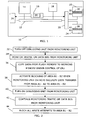
- An electronic data processing device 10 according to a first embodiment of the invention is shown in a block schematic in fig. 1.
- the device is preferably provided in a portable communication device and in the preferred embodiment the device is provided in a cellular phone and then a so-called smartphone.
- a cellular phone is just one example of where the invention can be implemented.
- the invention can for instance also be used in a PDA (personal digital assistant), a palm top computer, a lap top computer and in a PC (personal Computer).
- the device where the electronic data processing device according to the invention is implemented should however have functionality for secure transferring and transactions.
- the device 10 includes a communication bus 12 to which are connected a central processing unit 14, a device for blocking write attempts 16, a ROM memory 18 and an interface 20 towards external memories.
- the device 16 includes a monitoring unit 28, the functioning of which will be described in more detail layer.
- a working memory 22 which preferably is a volatile so-called SD RAM memory and a non-volatile NAND flash memory 24.
- a debugging unit 26 is also connected to the bus 12.
- the NAND flash memory includes an area defined by memory addresses A1 and A2, which area comprises security data 30 in the form of private cryptographic keys.
- the working memory 22 includes a corresponding area defined by memory addresses B1 and B2, which is to receive the private security keys.
- the main functioning of the electronic data processing device is, as is well known to the man skilled in the art, to execute software stored in different memories under the control of the central processing unit.
- Some such software can be some type of transactions software originally stored in the NAND flash memory.
- the information on a NAND flash memory cannot be used directly, but this information has to be transferred to a working memory before being used. If this is done in a straight-forward way, without taking necessary precautions, this data can be tampered with, which is highly undesirable if the data includes private keys to be used in for instance transactions involving money.
- One such source of tampering can be the debugging unit, which is connected to the device in order to debug faulty programs. This debugging unit often has contact with other devices, like computers and servers and can take control of the central processing unit of the electronic processing device and is therefore a potential safety risk for the data that is transferred.
- the device and method according to a first embodiment of the invention takes care of some of these safety aspects. Therefore the performance of the device according to this first embodiment will now be explained with reference being made to fig. 2, which shows a flow chart of a method according to this first embodiment of the invention.
- the data in the flash memory 24 has to be transferred to the working memory 22, which in this first embodiment is done under the control of the central processing unit 14.
- the monitoring unit 28 in device for blocking write attempts 16 disconnects or turns off the debugging unit 26, step 32, in order to safeguard that the security keys in the flash memory 24 will not be tampered with after copying. This turning off is thus done independently from the central processing unit 14.
- the monitoring unit 28 monitors the traffic on the bus 12, step 34. Traffic on the bus is sent using source and destination addresses.
- This unit 14 therefore controls the ROM memory 18, which includes transferral codes for transferring all the data in the flash memory 24 to the working memory 22.
- the data from the flash memory 24 can be stored in any position in the working memory 22.
- the content of the flash memory 24 is transferred sequentially.
- the monitoring unit 28 is set to look out for the memory addresses A1 and A2 defining the area of the security keys 30 in the flash memory on the data bus 12. This information is pre-set and pre-stored in the monitoring unit 28 and therefore provided beforehand in the monitoring unit 28.
- the monitoring unit begins activating blocking through storing the destination address B1. It then waits until the last address A2 of the area is transferred to destination address B2, which it also stores.
- the monitoring unit then locks the data area B1 - B2 of the working memory 22, since then the keys 30 have been copied.
- Fig. 3 shows a device 10 that is similar to the device in fig. 1.
- the device for blocking write attempts 16 also includes a copy control unit 46.
- This unit 46 which in this embodiment is a DMA (Direct Memory Access) unit, takes care of the transfer of the keys in the area A1 - A2 in the flash memory 24 to the area B1 - B2 of the working memory 22.
- the monitoring unit 28 in device 16 here disconnects or turns off the debugging unit 26, step 48, in order to safeguard that the private security keys 30 in the flash memory 24 will not be tampered with after copying.
- the copy control unit 46 copies the keys 30 in the area defined by addresses A1 and A2 in the flash memory 24 to the area defined by addresses B1 and B2 in the working memory 22, step 50.
- both the addresses A1 - A2 and addresses B1 - B2 are pre-defined and pre-stored in the copy control unit 46 and therefore provided beforehand.
- the copy control unit 46 here also transfer this content sequentially.
- the copy control unit 46 has copied these addresses it notifies the monitoring unit 28, which then goes on and activates blocking of the area defined by addresses B1 and B2, step 52.
- the monitoring unit 28 can also have these addresses B1 and B2 pre-stored or receive them from the copy control unit 46 upon signalling of finished copying.
- the monitoring unit 28 then reconnects or turns on the debugging unit 26, step 54, so that it can function yet again. Thereafter the monitoring unit 28 starts monitoring all the traffic on the data bus, step 56.
- the central processing unit 14 transfers the rest of the content from the flash memory 24 to the working memory 22, step 58, which is done in the same way as was described in relation to the first embodiment.
- the monitoring unit 28 then blocks all attempts to write to the area defined by addresses B1 and B2, step 60. This blocking is done in the same way as was described in the first embodiment. Steps 48 - 56 and 60 are all performed by the monitoring unit independently of the central processing unit.
- the device for blocking write attempts 16 including the copy control unit 46 and the monitoring unit 28 is also here provided in the form of hardware for making illegal tampering of the device hard, so that write-protection of the moved security keys can be guaranteed.
- the working memory is emptied, which means that the data in the flash memory has to be transferred each time the device is turned on again or rebooted.
- the present invention has many advantages. It enables the storage of the private security keys in a working memory without risking tampering of these keys, which is guaranteed by the independence of the central processing units. Another advantage is that cheaper memories therefore can be used instead of the memories that would otherwise be needed. It also allows the possibility to keep a debugging unit in the device for debugging software loaded in the device without having to compromise the safety of the security keys.
- the present invention can be varied in many ways. The different method steps do not necessarily all have to be provided in the order described. It is however essential that the debugging unit is turned off before the keys are transferred and that the activating of a blocking or locking follows immediately after the transfer of the keys.
- the flash memory can be included in the device or be an external memory that is connected to the device. It can also include other data than the keys and any software associated with the keys.
- the working memory can of course also include other types of information. It is possible that the flash memory, in the first described embodiment can have the addresses of the defined area in the working memory stored at a specific location, which location the ROM memory then can access for finding out the destination address of the security keys.
- the invention is furthermore not limited to private security keys, but can be applied on any data that needs to be write-protected. In view of this the present invention is therefore only to be limited by the following claims.
Landscapes
- Engineering & Computer Science (AREA)
- Theoretical Computer Science (AREA)
- Computer Security & Cryptography (AREA)
- Computer Hardware Design (AREA)
- Software Systems (AREA)
- Physics & Mathematics (AREA)
- General Engineering & Computer Science (AREA)
- General Physics & Mathematics (AREA)
- Storage Device Security (AREA)
- Techniques For Improving Reliability Of Storages (AREA)
- Debugging And Monitoring (AREA)
- Arrangements For Transmission Of Measured Signals (AREA)
Claims (19)
- Verfahren zum Übertragen von Daten aus einem nichtflüchtigen Speicher (24) in einen Arbeitsspeicher (22) einer elektronischen Datenverarbeitungsvorrichtung (10) mit den folgenden Schritten:Kopieren von Sicherheitsdaten (30) von dem nichtflüchtigen Speicher in den Arbeitsspeicher, wobei die Sicherheitsdaten schreibgeschützt sein sollen (Schritte 36; 50, 58),Aktivieren einer Blockierfunktion für die Sicherheitsdaten in dem Arbeitsspeicher (Schritt 38; 52), wobei der Schritt des Aktivierens durch das Kopieren in den Arbeitsspeicher getriggert wird;Überwachen der gesamten Kommunikation mit dem Arbeitsspeicher (Schritte 34, 42; 56), undBlockieren aller Schreibversuche auf die kopierten Sicherheitsdaten, die in dem Arbeitsspeicher gespeichert sind, gemäß der Blockierfunktion (Schritte 44; 60),wobei zumindest die Schritte des Aktivierens einer Blockierfunktion, des Überwachens der Kommunikation und des Blockierens der Schreibversuche unabhängig von der Zentralverarbeitungseinheit (14) der Datenverarbeitungsvorrichtung durchgeführt werden, so dass die Zentralverarbeitungseinheit die Sicherheitsdaten nicht manipulieren kann.
- Verfahren nach Anspruch 1, wobei der Bereich (A1, A2) der Sicherheitsdaten in dem nichtflüchtigen Speicher in einer Vorrichtung zum Blockieren von Schreibversuchen (16) vordefiniert und vorab gespeichert wird und zumindest mit Bezug zu dem Aktivieren einer Blockierfunktion verwendet wird.
- Verfahren nach Anspruch 1 oder 2, wobei der Schritt des Kopierens von Daten das Kopieren lediglich der Sicherheitsdaten von dem nichtflüchtigen Speicher in den Arbeitsspeicher unabhängig von der Zentralverarbeitungseinheit der Datenverarbeitungsvorrichtung (Schritt 50) und das Kopieren von weiteren Daten unter der Steuerung der Zentralverarbeitungseinheit der Vorrichtung (Schritt 58) umfasst.
- Verfahren nach Anspruch 3, wobei der Bereich (A1, A2) der Sicherheitsdaten in dem nichtflüchtigen Speicher und der Bereich (B1, B2) für den Speicher der Sicherheitsdaten in dem Arbeitsspeicher vordefiniert wird, und wobei der Schritt des Aktivierens einer Blockierfunktion durch das Kopieren in den vorbestimmten Bereich in dem Arbeitsspeicher getriggert wird, und wobei die Blockierfunktion für diesen Bereich des Arbeitsspeichers aktiviert wird.
- Verfahren nach Anspruch 1 oder 2, wobei der Schritt des Kopierens das Kopieren der gesamten Daten von dem nichtflüchtigen Speicher in den Arbeitsspeicher unter der Steuerung der Zentralverarbeitungseinheit der Vorrichtung (Schritt 36) umfasst.
- Verfahren nach Anspruch 5, wobei der Bereich (A1, A2) der Sicherheitsdaten in dem nichtflüchtigen Speicher vordefiniert wird und wobei der Schritt des Aktivierens einer Blockierfunktion durch eine erste Detektion des Kopierens von Sicherheitsdaten von dem vorbestimmten Bereich in den nichtflüchtigen Speicher in einen Bereich (B1, B2) des Arbeitsspeichers getriggert wird und wobei die Blockierfunktion für diesen Bereich des Arbeitsspeichers aktiviert wird.
- Verfahren nach einem der vorangehenden Ansprüche, wobei die Blockierfunktion das Ändern der Zieladresse der in den Arbeitsspeicher übertragenen Daten umfasst.
- Verfahren nach einem der vorangehenden Ansprüche, das weiterhin die Schritte des Trennens einer Debugger-Einheit (Schritt 32; 48) umfasst, zumindest wenn die Sicherheitsdaten in den Arbeitsspeicher kopiert werden, und das erneute Verbinden der Debugger-Einheit (Schritt 40; 54), wenn die Blockierfunktion aktiviert worden ist.
- Vorrichtung (16) zum Blockieren von Schreibversuchen auf Sicherheitsdaten (30), die von einem nichtflüchtigen Speicher (24) in einen Arbeitsspeicher (22) in einer elektronischen Datenverarbeitungseinrichtung (10), die eine Zentralverarbeitungseinheit (14) umfasst, übertragen werden, und die eine Überwachungseinheit (28) umfasst, die ausgebildet ist, um:eine Blockierfunktion zum Blockieren von Sicherheitsdaten in dem Arbeitsspeicher zu aktivieren, wobei die Aktivierung durch ein Kopieren der Sicherheitsdaten von dem nichtflüchtigen Speicher in den Arbeitsspeicher getriggert wird,die gesamte Kommunikation mit dem Arbeitsspeicher zu überwachen, undalle Schreibversuche auf die kopierten Sicherheitsdaten, die in dem Arbeitsspeicher gespeichert sind, gemäß der Blockierfunktion zu blockieren,wobei dieses vollständig unabhängig von der Zentralverarbeitungseinheit der Datenverarbeitungseinrichtung durchgeführt wird, so dass die Zentralverarbeitungseinheit die Sicherheitsdaten nicht manipulieren kann.
- Vorrichtung nach Anspruch 9, wobei der Bereich (A1, A2) der Sicherheitsdaten in dem nichtflüchtigen Speicher in der Vorrichtung vordefiniert und vorab gespeichert ist und mit Bezug auf mindestens das Aktivieren einer Blockierfunktion verwendet wird.
- Vorrichtung nach Anspruch 9 oder 10, die weiterhin eine Kopiersteuereinheit (46) umfasst, die ausgebildet ist, um die Sicherheitsdaten von dem nichtflüchtigen Speicher in den Arbeitsspeicher ebenfalls unabhängig von der Zentralverarbeitungseinheit der Datenverarbeitungseinrichtung zu kopieren.
- Vorrichtung nach Anspruch 11, wobei der Bereich (A1, A2) der Sicherheitsdaten in dem nichtflüchtigen Speicher und der Bereich (B1, B2) zum Speichern der Sicherheitsdaten in dem Arbeitsspeicher in der Vorrichtung vordefiniert und vorab gespeichert werden, und wobei die Überwachungseinheit durch das Kopieren in den vordefinierten Bereich in dem Arbeitsspeicher getriggert wird, wenn eine Blockierfunktion aktiviert wird, und wobei die Blockierfunktion für diesen Bereich des Arbeitsspeichers aktiviert wird.
- Vorrichtung nach Anspruch 9 oder 10, wobei der Bereich der Sicherheitsdaten (A1, A2) in dem nichtflüchtigen Speicher in der Vorrichtung vordefiniert und vorab gespeichert ist, und wobei die Überwachungseinheit, wenn eine Blockierfunktion aktiviert wird, durch eine erste Detektion des Kopierens von Sicherheitsdaten von dem vordefinierten Bereich in den nichtflüchtigen Speicher in einen Bereich (B1, B2) des Arbeitsspeichers getriggert wird und die Blockierfunktion für diesen Bereich des Arbeitsspeichers aktiviert wird.
- Vorrichtung nach einem der Ansprüche 9 bis 13, wobei die Blockierfunktion der Überwachungseinheit das Blockieren von Schreibversuchen umfasst, indem die Zieladresse der Daten, die in den Arbeitsspeicher übertragen werden, geändert wird.
- Vorrichtung nach einem der Ansprüche 9 bis 14, wobei die Überwachungseinheit ausgebildet ist, um eine Debugger-Einheit (26) von der elektronischen Datenverarbeitungseinrichtung zu trennen, zumindest wenn die Sicherheitsdaten in den Arbeitsspeicher kopiert werden, und um die Debugger-Einheit erneut zu verbinden, wenn das Blockieren aktiviert worden ist.
- Vorrichtung nach einem der Ansprüche 9 bis 15, wobei diese in Hardware implementiert wird.
- Elektronische Datenverarbeitungsvorrichtung (10) umfassend einen nichtflüchtigen Speicher (24), der Daten, einschließlich Sicherheitsdaten (30), die schreibgeschützt sein sollen, umfasst, einen Arbeitsspeicher (22), eine Zentralverarbeitungseinheit (14), die ausgebildet ist, um das Kopieren von mindestens einigen Daten aus dem nichtflüchtigen Speicher in den Arbeitsspeicher zu steuern, und eine Vorrichtung zum Blockieren von Schreibversuchen (16) auf Sicherheitsdaten gemäß einem der Ansprüche 9 bis 16 umfasst.
- Elektronische Datenverarbeitungsvorrichtung gemäß Anspruch 17, wobei die Vorrichtung ein tragbares Kommunikationsgerät ist.
- Elektronische Datenverarbeitungsvorrichtung nach Anspruch 18, wobei die Vorrichtung ein Mobiltelefon ist.
Priority Applications (9)
| Application Number | Priority Date | Filing Date | Title |
|---|---|---|---|
| EP03019882A EP1513039B1 (de) | 2003-09-02 | 2003-09-02 | Übertragung von sicherheitsrelevanten Daten zwischen zwei Speichern |
| DE60312159T DE60312159T2 (de) | 2003-09-02 | 2003-09-02 | Übertragung von sicherheitsrelevanten Daten zwischen zwei Speichern |
| AT03019882T ATE355565T1 (de) | 2003-09-02 | 2003-09-02 | Übertragung von sicherheitsrelevanten daten zwischen zwei speichern |
| JP2006524321A JP4739206B2 (ja) | 2003-09-02 | 2004-08-25 | 2つのメモリー間でのセキュリティデータの転送 |
| PCT/EP2004/009462 WO2005022366A1 (en) | 2003-09-02 | 2004-08-25 | Transfer of security data between two memories |
| KR1020067004303A KR101065904B1 (ko) | 2003-09-02 | 2004-08-25 | 두 메모리 사이의 보안성 데이터 전송 |
| US10/569,530 US7865739B2 (en) | 2003-09-02 | 2004-08-25 | Methods and devices for transferring security data between memories |
| BRPI0413866-0A BRPI0413866A (pt) | 2003-09-02 | 2004-08-25 | método de transferência de dados de uma memória não-volátil para uma memória de trabalho, dispositivo para bloquear de tentativas de escrita para dados de segurança, e, dispositivo para processamento de dados eletrÈnicos |
| CN200480025206.4A CN100478825C (zh) | 2003-09-02 | 2004-08-25 | 在两个存储器之间传输安全数据 |
Applications Claiming Priority (1)
| Application Number | Priority Date | Filing Date | Title |
|---|---|---|---|
| EP03019882A EP1513039B1 (de) | 2003-09-02 | 2003-09-02 | Übertragung von sicherheitsrelevanten Daten zwischen zwei Speichern |
Publications (2)
| Publication Number | Publication Date |
|---|---|
| EP1513039A1 EP1513039A1 (de) | 2005-03-09 |
| EP1513039B1 true EP1513039B1 (de) | 2007-02-28 |
Family
ID=34130102
Family Applications (1)
| Application Number | Title | Priority Date | Filing Date |
|---|---|---|---|
| EP03019882A Expired - Lifetime EP1513039B1 (de) | 2003-09-02 | 2003-09-02 | Übertragung von sicherheitsrelevanten Daten zwischen zwei Speichern |
Country Status (5)
| Country | Link |
|---|---|
| EP (1) | EP1513039B1 (de) |
| JP (1) | JP4739206B2 (de) |
| CN (1) | CN100478825C (de) |
| AT (1) | ATE355565T1 (de) |
| DE (1) | DE60312159T2 (de) |
Families Citing this family (2)
| Publication number | Priority date | Publication date | Assignee | Title |
|---|---|---|---|---|
| US10360143B2 (en) * | 2010-07-01 | 2019-07-23 | Qualcomm Incorporated | Parallel use of integrated non-volatile memory and main volatile memory within a mobile device |
| CN106775448A (zh) * | 2016-11-15 | 2017-05-31 | 航天信息股份有限公司 | 一种加密卡的文件存储方法及安全删除方法 |
Family Cites Families (8)
| Publication number | Priority date | Publication date | Assignee | Title |
|---|---|---|---|---|
| JPH01261760A (ja) * | 1988-04-13 | 1989-10-18 | Canon Inc | コンピュータ装置 |
| US5561817A (en) * | 1993-08-16 | 1996-10-01 | Thermo King Corporation | Method of securely controlling direct memory access (DMA) of a shared memory by a DMA device on an expansion board |
| US5491827A (en) * | 1994-01-14 | 1996-02-13 | Bull Hn Information Systems Inc. | Secure application card for sharing application data and procedures among a plurality of microprocessors |
| US6115819A (en) * | 1994-05-26 | 2000-09-05 | The Commonwealth Of Australia | Secure computer architecture |
| FR2725537B1 (fr) * | 1994-10-11 | 1996-11-22 | Bull Cp8 | Procede de chargement d'une zone memoire protegee d'un dispositif de traitement de l'information et dispositif associe |
| US5634099A (en) * | 1994-12-09 | 1997-05-27 | International Business Machines Corporation | Direct memory access unit for transferring data between processor memories in multiprocessing systems |
| US5825878A (en) * | 1996-09-20 | 1998-10-20 | Vlsi Technology, Inc. | Secure memory management unit for microprocessor |
| JP2000020401A (ja) * | 1998-07-07 | 2000-01-21 | Seiko Epson Corp | Cpu装置、情報処理装置およびその制御方法 |
-
2003
- 2003-09-02 EP EP03019882A patent/EP1513039B1/de not_active Expired - Lifetime
- 2003-09-02 AT AT03019882T patent/ATE355565T1/de not_active IP Right Cessation
- 2003-09-02 DE DE60312159T patent/DE60312159T2/de not_active Expired - Lifetime
-
2004
- 2004-08-25 JP JP2006524321A patent/JP4739206B2/ja not_active Expired - Fee Related
- 2004-08-25 CN CN200480025206.4A patent/CN100478825C/zh not_active Expired - Fee Related
Also Published As
| Publication number | Publication date |
|---|---|
| CN1846187A (zh) | 2006-10-11 |
| JP2007504521A (ja) | 2007-03-01 |
| DE60312159T2 (de) | 2007-10-31 |
| JP4739206B2 (ja) | 2011-08-03 |
| ATE355565T1 (de) | 2006-03-15 |
| DE60312159D1 (de) | 2007-04-12 |
| EP1513039A1 (de) | 2005-03-09 |
| CN100478825C (zh) | 2009-04-15 |
Similar Documents
| Publication | Publication Date | Title |
|---|---|---|
| US11507654B2 (en) | Secure environment in a non-secure microcontroller | |
| EP2263187B1 (de) | Peripheriegerät mit sperrmechanismus | |
| JP6306578B2 (ja) | メモリ保護装置及び保護方法 | |
| CN1182678C (zh) | 安全引导 | |
| KR100319677B1 (ko) | 메모리액세스제어회로 | |
| CN107003936B (zh) | 具有非可读页的存储器保护 | |
| JP5114617B2 (ja) | 秘密鍵を保護する、セキュア端末、プログラム、および方法 | |
| US7523279B2 (en) | Information processing apparatus for accessing memory spaces including a user memory space and a secure memory space | |
| WO2004107176A1 (en) | Method and apparatus for determining access permission | |
| US20080263256A1 (en) | Logic Device with Write Protected Memory Management Unit Registers | |
| EP3084593B1 (de) | Aktualisierbarer funk in einem integrierten schaltkreis | |
| CN101084504A (zh) | 具有改进的器件安全性的集成电路 | |
| CA2381162C (en) | Data processing device having protected memory and corresponding method | |
| US7865739B2 (en) | Methods and devices for transferring security data between memories | |
| EP1513039B1 (de) | Übertragung von sicherheitsrelevanten Daten zwischen zwei Speichern | |
| KR102036256B1 (ko) | 보안성이 강화된 안드로이드 임베디드 보드 | |
| CN108009436B (zh) | 一种soc芯片的多用户管理方法、系统及soc芯片 | |
| CN106845296A (zh) | 一种保护密码的方法、系统及一种主板、连接器 | |
| TWI221070B (en) | Increasing code separation between applications |
Legal Events
| Date | Code | Title | Description |
|---|---|---|---|
| PUAI | Public reference made under article 153(3) epc to a published international application that has entered the european phase |
Free format text: ORIGINAL CODE: 0009012 |
|
| AK | Designated contracting states |
Kind code of ref document: A1 Designated state(s): AT BE BG CH CY CZ DE DK EE ES FI FR GB GR HU IE IT LI LU MC NL PT RO SE SI SK TR |
|
| AX | Request for extension of the european patent |
Extension state: AL LT LV MK |
|
| 17P | Request for examination filed |
Effective date: 20050826 |
|
| AKX | Designation fees paid |
Designated state(s): AT BE BG CH CY CZ DE DK EE ES FI FR GB GR HU IE IT LI LU MC NL PT RO SE SI SK TR |
|
| RIC1 | Information provided on ipc code assigned before grant |
Ipc: G06F 21/20 20060101AFI20060627BHEP |
|
| GRAP | Despatch of communication of intention to grant a patent |
Free format text: ORIGINAL CODE: EPIDOSNIGR1 |
|
| GRAS | Grant fee paid |
Free format text: ORIGINAL CODE: EPIDOSNIGR3 |
|
| GRAA | (expected) grant |
Free format text: ORIGINAL CODE: 0009210 |
|
| AK | Designated contracting states |
Kind code of ref document: B1 Designated state(s): AT BE BG CH CY CZ DE DK EE ES FI FR GB GR HU IE IT LI LU MC NL PT RO SE SI SK TR |
|
| PG25 | Lapsed in a contracting state [announced via postgrant information from national office to epo] |
Ref country code: CH Free format text: LAPSE BECAUSE OF FAILURE TO SUBMIT A TRANSLATION OF THE DESCRIPTION OR TO PAY THE FEE WITHIN THE PRESCRIBED TIME-LIMIT Effective date: 20070228 Ref country code: SI Free format text: LAPSE BECAUSE OF FAILURE TO SUBMIT A TRANSLATION OF THE DESCRIPTION OR TO PAY THE FEE WITHIN THE PRESCRIBED TIME-LIMIT Effective date: 20070228 Ref country code: AT Free format text: LAPSE BECAUSE OF FAILURE TO SUBMIT A TRANSLATION OF THE DESCRIPTION OR TO PAY THE FEE WITHIN THE PRESCRIBED TIME-LIMIT Effective date: 20070228 Ref country code: DK Free format text: LAPSE BECAUSE OF FAILURE TO SUBMIT A TRANSLATION OF THE DESCRIPTION OR TO PAY THE FEE WITHIN THE PRESCRIBED TIME-LIMIT Effective date: 20070228 Ref country code: NL Free format text: LAPSE BECAUSE OF FAILURE TO SUBMIT A TRANSLATION OF THE DESCRIPTION OR TO PAY THE FEE WITHIN THE PRESCRIBED TIME-LIMIT Effective date: 20070228 Ref country code: LI Free format text: LAPSE BECAUSE OF FAILURE TO SUBMIT A TRANSLATION OF THE DESCRIPTION OR TO PAY THE FEE WITHIN THE PRESCRIBED TIME-LIMIT Effective date: 20070228 Ref country code: FI Free format text: LAPSE BECAUSE OF FAILURE TO SUBMIT A TRANSLATION OF THE DESCRIPTION OR TO PAY THE FEE WITHIN THE PRESCRIBED TIME-LIMIT Effective date: 20070228 Ref country code: BE Free format text: LAPSE BECAUSE OF FAILURE TO SUBMIT A TRANSLATION OF THE DESCRIPTION OR TO PAY THE FEE WITHIN THE PRESCRIBED TIME-LIMIT Effective date: 20070228 |
|
| REG | Reference to a national code |
Ref country code: GB Ref legal event code: FG4D |
|
| REG | Reference to a national code |
Ref country code: CH Ref legal event code: EP |
|
| REF | Corresponds to: |
Ref document number: 60312159 Country of ref document: DE Date of ref document: 20070412 Kind code of ref document: P |
|
| REG | Reference to a national code |
Ref country code: IE Ref legal event code: FG4D |
|
| PG25 | Lapsed in a contracting state [announced via postgrant information from national office to epo] |
Ref country code: BG Free format text: LAPSE BECAUSE OF EXPIRATION OF PROTECTION Effective date: 20070529 |
|
| PG25 | Lapsed in a contracting state [announced via postgrant information from national office to epo] |
Ref country code: SE Free format text: LAPSE BECAUSE OF FAILURE TO SUBMIT A TRANSLATION OF THE DESCRIPTION OR TO PAY THE FEE WITHIN THE PRESCRIBED TIME-LIMIT Effective date: 20070531 |
|
| PG25 | Lapsed in a contracting state [announced via postgrant information from national office to epo] |
Ref country code: ES Free format text: LAPSE BECAUSE OF FAILURE TO SUBMIT A TRANSLATION OF THE DESCRIPTION OR TO PAY THE FEE WITHIN THE PRESCRIBED TIME-LIMIT Effective date: 20070608 |
|
| PG25 | Lapsed in a contracting state [announced via postgrant information from national office to epo] |
Ref country code: PT Free format text: LAPSE BECAUSE OF FAILURE TO SUBMIT A TRANSLATION OF THE DESCRIPTION OR TO PAY THE FEE WITHIN THE PRESCRIBED TIME-LIMIT Effective date: 20070730 |
|
| NLV1 | Nl: lapsed or annulled due to failure to fulfill the requirements of art. 29p and 29m of the patents act | ||
| ET | Fr: translation filed | ||
| REG | Reference to a national code |
Ref country code: CH Ref legal event code: PL |
|
| PG25 | Lapsed in a contracting state [announced via postgrant information from national office to epo] |
Ref country code: SK Free format text: LAPSE BECAUSE OF FAILURE TO SUBMIT A TRANSLATION OF THE DESCRIPTION OR TO PAY THE FEE WITHIN THE PRESCRIBED TIME-LIMIT Effective date: 20070228 |
|
| PG25 | Lapsed in a contracting state [announced via postgrant information from national office to epo] |
Ref country code: CZ Free format text: LAPSE BECAUSE OF FAILURE TO SUBMIT A TRANSLATION OF THE DESCRIPTION OR TO PAY THE FEE WITHIN THE PRESCRIBED TIME-LIMIT Effective date: 20070228 Ref country code: RO Free format text: LAPSE BECAUSE OF FAILURE TO SUBMIT A TRANSLATION OF THE DESCRIPTION OR TO PAY THE FEE WITHIN THE PRESCRIBED TIME-LIMIT Effective date: 20070228 |
|
| PLBE | No opposition filed within time limit |
Free format text: ORIGINAL CODE: 0009261 |
|
| STAA | Information on the status of an ep patent application or granted ep patent |
Free format text: STATUS: NO OPPOSITION FILED WITHIN TIME LIMIT |
|
| 26N | No opposition filed |
Effective date: 20071129 |
|
| PG25 | Lapsed in a contracting state [announced via postgrant information from national office to epo] |
Ref country code: GR Free format text: LAPSE BECAUSE OF FAILURE TO SUBMIT A TRANSLATION OF THE DESCRIPTION OR TO PAY THE FEE WITHIN THE PRESCRIBED TIME-LIMIT Effective date: 20070529 Ref country code: IT Free format text: LAPSE BECAUSE OF FAILURE TO SUBMIT A TRANSLATION OF THE DESCRIPTION OR TO PAY THE FEE WITHIN THE PRESCRIBED TIME-LIMIT Effective date: 20070228 Ref country code: MC Free format text: LAPSE BECAUSE OF NON-PAYMENT OF DUE FEES Effective date: 20070930 |
|
| PG25 | Lapsed in a contracting state [announced via postgrant information from national office to epo] |
Ref country code: IE Free format text: LAPSE BECAUSE OF NON-PAYMENT OF DUE FEES Effective date: 20070903 |
|
| PG25 | Lapsed in a contracting state [announced via postgrant information from national office to epo] |
Ref country code: EE Free format text: LAPSE BECAUSE OF FAILURE TO SUBMIT A TRANSLATION OF THE DESCRIPTION OR TO PAY THE FEE WITHIN THE PRESCRIBED TIME-LIMIT Effective date: 20070228 |
|
| PG25 | Lapsed in a contracting state [announced via postgrant information from national office to epo] |
Ref country code: CY Free format text: LAPSE BECAUSE OF FAILURE TO SUBMIT A TRANSLATION OF THE DESCRIPTION OR TO PAY THE FEE WITHIN THE PRESCRIBED TIME-LIMIT Effective date: 20070228 |
|
| PG25 | Lapsed in a contracting state [announced via postgrant information from national office to epo] |
Ref country code: LU Free format text: LAPSE BECAUSE OF NON-PAYMENT OF DUE FEES Effective date: 20070902 |
|
| PG25 | Lapsed in a contracting state [announced via postgrant information from national office to epo] |
Ref country code: TR Free format text: LAPSE BECAUSE OF FAILURE TO SUBMIT A TRANSLATION OF THE DESCRIPTION OR TO PAY THE FEE WITHIN THE PRESCRIBED TIME-LIMIT Effective date: 20070228 Ref country code: HU Free format text: LAPSE BECAUSE OF FAILURE TO SUBMIT A TRANSLATION OF THE DESCRIPTION OR TO PAY THE FEE WITHIN THE PRESCRIBED TIME-LIMIT Effective date: 20070901 |
|
| REG | Reference to a national code |
Ref country code: FR Ref legal event code: PLFP Year of fee payment: 14 |
|
| REG | Reference to a national code |
Ref country code: FR Ref legal event code: PLFP Year of fee payment: 15 |
|
| REG | Reference to a national code |
Ref country code: FR Ref legal event code: PLFP Year of fee payment: 16 |
|
| PGFP | Annual fee paid to national office [announced via postgrant information from national office to epo] |
Ref country code: NO Payment date: 20180913 Year of fee payment: 7 |
|
| PGFP | Annual fee paid to national office [announced via postgrant information from national office to epo] |
Ref country code: GB Payment date: 20180829 Year of fee payment: 16 |
|
| GBPC | Gb: european patent ceased through non-payment of renewal fee |
Effective date: 20190902 |
|
| PG25 | Lapsed in a contracting state [announced via postgrant information from national office to epo] |
Ref country code: GB Free format text: LAPSE BECAUSE OF NON-PAYMENT OF DUE FEES Effective date: 20190902 Ref country code: FR Free format text: LAPSE BECAUSE OF NON-PAYMENT OF DUE FEES Effective date: 20190930 |
|
| PGFP | Annual fee paid to national office [announced via postgrant information from national office to epo] |
Ref country code: DE Payment date: 20200819 Year of fee payment: 18 |
|
| REG | Reference to a national code |
Ref country code: DE Ref legal event code: R119 Ref document number: 60312159 Country of ref document: DE |
|
| PG25 | Lapsed in a contracting state [announced via postgrant information from national office to epo] |
Ref country code: DE Free format text: LAPSE BECAUSE OF NON-PAYMENT OF DUE FEES Effective date: 20220401 |