EP1511264B1 - Adaptive imbalance correction based on amplitude distribution - Google Patents
Adaptive imbalance correction based on amplitude distribution Download PDFInfo
- Publication number
- EP1511264B1 EP1511264B1 EP04019674A EP04019674A EP1511264B1 EP 1511264 B1 EP1511264 B1 EP 1511264B1 EP 04019674 A EP04019674 A EP 04019674A EP 04019674 A EP04019674 A EP 04019674A EP 1511264 B1 EP1511264 B1 EP 1511264B1
- Authority
- EP
- European Patent Office
- Prior art keywords
- modulation
- amplitude
- probability density
- complex signal
- amplitude probability
- Prior art date
- Legal status (The legal status is an assumption and is not a legal conclusion. Google has not performed a legal analysis and makes no representation as to the accuracy of the status listed.)
- Expired - Lifetime
Links
- 230000003044 adaptive effect Effects 0.000 title description 5
- 238000012937 correction Methods 0.000 title description 5
- 238000000034 method Methods 0.000 claims abstract description 24
- 230000006735 deficit Effects 0.000 claims abstract description 14
- 230000006872 improvement Effects 0.000 abstract description 2
- 230000008569 process Effects 0.000 description 10
- 230000010354 integration Effects 0.000 description 8
- 238000010586 diagram Methods 0.000 description 7
- 230000000694 effects Effects 0.000 description 6
- 230000008859 change Effects 0.000 description 4
- 230000006870 function Effects 0.000 description 4
- 230000001186 cumulative effect Effects 0.000 description 3
- 230000007812 deficiency Effects 0.000 description 3
- 230000001419 dependent effect Effects 0.000 description 3
- 238000001514 detection method Methods 0.000 description 3
- 238000009825 accumulation Methods 0.000 description 2
- 230000005540 biological transmission Effects 0.000 description 2
- 238000006243 chemical reaction Methods 0.000 description 2
- 238000004891 communication Methods 0.000 description 2
- 230000007246 mechanism Effects 0.000 description 2
- 230000004044 response Effects 0.000 description 2
- 238000004088 simulation Methods 0.000 description 2
- 230000032683 aging Effects 0.000 description 1
- 238000013459 approach Methods 0.000 description 1
- 230000006399 behavior Effects 0.000 description 1
- 238000007796 conventional method Methods 0.000 description 1
- 230000003247 decreasing effect Effects 0.000 description 1
- 238000013507 mapping Methods 0.000 description 1
- 239000011159 matrix material Substances 0.000 description 1
- 238000010606 normalization Methods 0.000 description 1
- 230000001105 regulatory effect Effects 0.000 description 1
- 238000005070 sampling Methods 0.000 description 1
- 239000007787 solid Substances 0.000 description 1
- 238000001228 spectrum Methods 0.000 description 1
- 238000012360 testing method Methods 0.000 description 1
- 230000009466 transformation Effects 0.000 description 1
Images


Classifications
-
- H—ELECTRICITY
- H04—ELECTRIC COMMUNICATION TECHNIQUE
- H04L—TRANSMISSION OF DIGITAL INFORMATION, e.g. TELEGRAPHIC COMMUNICATION
- H04L27/00—Modulated-carrier systems
- H04L27/32—Carrier systems characterised by combinations of two or more of the types covered by groups H04L27/02, H04L27/10, H04L27/18 or H04L27/26
- H04L27/34—Amplitude- and phase-modulated carrier systems, e.g. quadrature-amplitude modulated carrier systems
- H04L27/36—Modulator circuits; Transmitter circuits
- H04L27/362—Modulation using more than one carrier, e.g. with quadrature carriers, separately amplitude modulated
- H04L27/364—Arrangements for overcoming imperfections in the modulator, e.g. quadrature error or unbalanced I and Q levels
-
- H—ELECTRICITY
- H04—ELECTRIC COMMUNICATION TECHNIQUE
- H04L—TRANSMISSION OF DIGITAL INFORMATION, e.g. TELEGRAPHIC COMMUNICATION
- H04L27/00—Modulated-carrier systems
- H04L27/0014—Carrier regulation
- H04L2027/0016—Stabilisation of local oscillators
-
- H—ELECTRICITY
- H04—ELECTRIC COMMUNICATION TECHNIQUE
- H04L—TRANSMISSION OF DIGITAL INFORMATION, e.g. TELEGRAPHIC COMMUNICATION
- H04L27/00—Modulated-carrier systems
- H04L27/0014—Carrier regulation
- H04L2027/0018—Arrangements at the transmitter end
Definitions
- the invention relates to a method for measuring and optimising critical parameters of a modulator in a communication system which utilise multilevel constellations e.g. QAM.
- the adjustment is performed during normal operation of the system.
- disturbance of the reception can occur in more or less degree, depending on the structure of the demodulator.
- One aspect of the problem is the individual differences from unit to unit. This can be handled by an individual tuning procedure. More serious, however, is drift of the impairments caused by a shift in temperature, LO (carrier) frequency or ageing while the equipment is in normal service. In order to handle this, an adaptive mechanism is required.
- EP0617532 to Nokia Corporation teaches a vector modulation system and a radio telephone comprising the vector modulation system adapted to correct or compensate amplitude and phase differences in a modulated data signal generated by a quadrature modulator, by measuring narrow band envelope powers at first and second selected frequencies of the signal, and generating a compensation or correction signal based on a comparison of the measured narrow band envelope powers at the first and second selected frequencies.
- the present invention provides a method for optimizing the performance of a modulator device, the features of which method are recited in the accompanying independent patent claim 1.
- the present invention provides an apparatus for optimizing the performance of a modulator device, the features of which apparatus are recited in the accompanying independent patent claim 3.
- the present invention provides a solution that includes a simple digital implementation that does not have specific requirements for high-speed AD/DA (analog-to-digital/digital-to-analog) devices or critical timing, which otherwise would represent a problem in conventional techniques utilising correlation methods.
- AD/DA analog-to-digital/digital-to-analog
- ⁇ is the frequency of the carrier
- r(t) is the amplitude
- ⁇ (t) the phase of the modulating signal
- This expression basically shows how amplitude and phase are modulated onto the carrier.
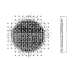
- FIG. 3 A 128 cross constellation ( as constituted by a twelve by twelve matrix with four elements omitted at each of the outer corners) is shown, with the grayscale shaded areas conceptually indicating the probability density for the vector to be in a given position in the modulation space at a selected point in time, denoted by "t".
- the reference system is drawn in solid lines.
- Fig. 4 we first observe that the constellation has an angular structure, implying that the circular indications of probability density used to illustrate are not giving an exact and correct picture of the situation.
- the inventors have found that a first-order estimate of distortions can be based on a rotational invariant probability distribution in modulation space, as represented by the gray shaded areas in figure 3 .
- altough the illustration given in figure 3 with different shades of gray for different probability density values indicate a stepwise variation, the variation typically is smooth and continuous.
- the stepped appearance generally is due to a resolution limitation of the tool used to generate the graphical illustration.
- the inventors have performed simulations to show the relative frequency of the different amplitudes occuring in the modulation space, by computing integration of the density for a large number of amplitudes for to different conditions of impairments, with results as shown in Fig. 4 .
- the curve diagrams generally indicate that the probability density of having a particular amplitude occuring increases almost linearly over a significant amplitude range. Since the amplitude frequency (i.e.
- the rate at which a particular amplitude occurs may be interpreted as the result of performing an integration of the probability density for a particular phase and amplitude in the modulation space, around the circle defined by the amplitude, the shades of gray that are shown in figure 3 has support to be understood as a "colour picture" wherein a particular color is indicative of a corresponding probability density.
- colour picture wherein a particular color is indicative of a corresponding probability density.
- FIG 3 an example of a circle for integration at one particular amplitude in a case with no significant LO leakage is indicated by a circle drawn in solid, while a circle for integration at a corresponding amplitude in a case with some LO leakage is indicated by a circle drawn in a broken line.
- impairments such as e.g. I/Q orthogonality error or I/Q gain difference
- the distribution indicated in fig 3 could be further distorted into e.g. an elliptic shape, which again by comptuing the integration around circles for various amplitudes would lead to a differently shaped amplitude distribution curve than those already shown in fig. 4 .
- the effect of this understanding is that if the origin is shifted slightly, like an LO leakage would do, one should not expect to see changes in the lower part of the envelope amplitude distribution curve.
- the inventors have found that at some point along the curve, with LO-leakage present, the resulting "modified" distribution curve B falls below the "original" curve A (i.e. the distribution curve generated from data representing no significant LO leakage), while becoming higher towards the upper end.
- a quadrature error is understood to mean that when mapping the component functions onto a plane, the coordinate axes are not orthogonal. If we assume that the I- component is aligned with an orthogonal coordinate system x,y, we can say that the Q- component has an angle ⁇ with the I-axis. The effect ⁇ not being 90° is that the circular indications of probability are reshaped to become ellipses. As every area element is reduced by cos ⁇ by this transformation, the probability density in every mapped point is inversely scaled.
- V OPT the point of intersection
- E C will be a good measure for the wanted "tail area" ifN is made sufficiently large.
- the estimate for E C will in a practical implementation be extracted from the envelope of the RF signal. Feeding the envelope to a comparator and setting the reference to E Thresh will give us the desired c(t).
- This two state signal i.e. c(t)
- the solution to the imbalance problem is then reduced to the task of minimising E C with respect to (i), (ii) and (iii). This can be done by varying the three imbalance parameters and measure the corresponding change in E C .
- a possible process for this is shown in Fig. 2 .
- An alternative process may be employed with the same detector solution, however, giving a different response pattern. The essential part, though, is to use the detector output information in a valid manner.
- Fig. 1 shows a simplified block diagram of a quadrature modulator with an exemplary embodyment of the invention.
- I- and Q-data are entering the block with reference number 20.
- This block performs a traditional quadrature adjustment by adding controlled cross talk of I onto Q and vice versa.
- I- and Q-channel gain are scaled by a factor with opposite sign for I-and Q-channel.
- the magnitude of both quadrature and gain adjustment are output from 10.
- I- and Q-data are further passed on to D/A converters 60 and the ordinary unwanted images from the conversion process are filtered in 80 before the signal is converted to RF or IF in 100 .
- the conversion stage is done in quadrature, meaning that the local oscillator signal from 90 is phase shifted in 110 so that the LO feeding the Q-channel mixer is 90° out of phase with respect to the LO feeding the I-channel mixer.
- a diode-based detector 130 will give us a squared estimate of the envelope, but as long as the response is monotonic this satisfies our needs.
- the output from 130 is split and one part led to a comparator 120 .
- the envelope is compared to a configurable threshold from 55. This threshold can be thought of as a trigger on the envelope: If the instantaneous envelope value is above the trigger, a logical 1 is the output from 120 , otherwise a logical 0 is the output.
- This comparator value is sampled and accumulated in the digital domain in 30 according to Equation 4. After each NT second the adaptive process for imbalance correction 10 receives a new estimate for E C and outputs an adjustment.
- Block 10 has four outputs for adjustment of imbalance according to (i),(ii) and (iii), where the LO leakage occupies two of the outputs.
- DC_I and DC_Q are converted to analogue DC voltages at the output of 50 and applied as DC correction voltages at the input stage of 100 .
- the other branch from the envelope detector 130 is low pass filtered in 140 and so that the mean value of the RF signal is extracted and sampled in 70. This information is required in order to ensure that the E Thresh parameter approximately follows gain variations of the IF/RF signal.
- the E Thresh is continuously adjusted in the Envelope Threshold Compensation block 40. Denote the output from 70 as E MEAN .
- the inventors have found that good correspondence with Vopt is achieved by setting the value of A to about 4 dB. The optimum setting of A and C is reached when a gain difference at IF/RF has minimum impact on the estimate for E C .
- a new parameter value is computed and applied to the hardware. Then the accumulate time window counter ATW is started in 13 to keep track of the configurable integration time. The next step 14 samples and accumulates the comparator output according to Equation 4.
- the Env_Count variable is equivalent to E c except for the lack of normalisation. This accumulation is performed until the test in block 15 indicates that the ATW counter has reached the integration time NT. A comparison of the current Env_count against the stored Env_count from last iteration is performed in 16 . If the new estimate is greater than the old, we are obviously moving the parameter in the wrong direction and hence the direction property for this parameter is inverted in 17 so that the next time the parameter is tuned it will be in an opposite direction of the current one.
- the adjustment of the parameter is temporarily stopped and the parameter selector k, increases by one, meaning that a different parameter will be tuned next time. k wraps around when it reaches 3. If the output from 15 is NO, the adjustment was successful and no change of direction or parameter is performed. The process ends up in 18 where the obtained estimate gets status as the old estimate. This means that the process has a memory of one envelope count estimate. The process then goes into an infinite loop back to 12 . In this way we cycle through the four parameters and perform an independent adjustment of each.
- the described system can be improved by introducing a enable/disable signal for the Env_Count accumulation variable.
- the idea is to enable counting only when the modulation trajectory corresponds to certain transmitted symbol sequences, e.g. selected corner points when detecting quadrature error.
- ⁇ Env_count Env_count-Env_Count_Old.
- This delta information can be used to define a variable step size for the parameters. Another way to improve the variance is to have larger memory on the Env_Count variable.
Landscapes
- Engineering & Computer Science (AREA)
- Computer Networks & Wireless Communication (AREA)
- Signal Processing (AREA)
- Digital Transmission Methods That Use Modulated Carrier Waves (AREA)
- Transmitters (AREA)
- Optical Communication System (AREA)
- Ultra Sonic Daignosis Equipment (AREA)
- Variable-Direction Aerials And Aerial Arrays (AREA)
Abstract
Description
- The invention relates to a method for measuring and optimising critical parameters of a modulator in a communication system which utilise multilevel constellations e.g. QAM. The adjustment is performed during normal operation of the system.
- In the field of digital communication, a common technique is to modulate a carrier with in-phase (I) and quadrature-phase (Q) data. Even though completely digital solutions exist, their practical use is often limited by the fact that a high sampling rate is required to generate a reasonably high carrier frequency. It is therefore still preferable for many applications, such as e.g. direct modulation on the transmission frequency, to perform this operation by means of a conventional modulator (mixer) operating in the analogue domain.
- In the analog process mentioned above, some deficiencies, not found in its digital counterpart, are typical. The invention focuses on correction of the three principal impairments of quadrature modulators:
- (i) Carrier wave leakage at the output of the modulator. Applying a variable DC source at the baseband input of the modulator can compensate for this.
- (ii) Differences in I- and Q-channel gain from DAC through modulator will cause mismatch between I- and Q signal levels. Scaling the baseband I and Q can align the level of the two components.
- (iii) The 0°/90° phase alignment of I and Q in the analogue modulator will not be precise, and imbalance will cause a loss of orthogonality between the I- and Q axis. This can be mitigated by cross-leakage between the baseband I and Q components
- In all cases disturbance of the reception can occur in more or less degree, depending on the structure of the demodulator.
- One aspect of the problem is the individual differences from unit to unit. This can be handled by an individual tuning procedure. More serious, however, is drift of the impairments caused by a shift in temperature, LO (carrier) frequency or ageing while the equipment is in normal service. In order to handle this, an adaptive mechanism is required.
- Of the three listed impairments, (i) is the most crucial to handle in a transmitter, as this more readily may cause a conflict with the regulatory spectrum mask requirements than (ii) and (iii).
- The aforementioned problems have been known for some time, and various techniques exist for adjusting and minimising such deficiencies.
-
EP0617532 to Nokia Corporation teaches a vector modulation system and a radio telephone comprising the vector modulation system adapted to correct or compensate amplitude and phase differences in a modulated data signal generated by a quadrature modulator, by measuring narrow band envelope powers at first and second selected frequencies of the signal, and generating a compensation or correction signal based on a comparison of the measured narrow band envelope powers at the first and second selected frequencies. - Four drawings are included to support the understanding of the invention.
-
Fig. 1 is a functional block diagram of a modulator comprising a compensation of imperfections according to the invention. -
Fig. 2 is a flow diagram describing a possible adaptive process for adjustment of the imbalance compensation. -
Fig. 3 shows a 128 QAM cross constellation and the influence of a DC offset due to an LO leakage component. -
Fig. 4 shows the amplitude distribution change due to an LO leakage component. - The present invention provides a method for optimizing the performance of a modulator device, the features of which method are recited in the accompanying
independent patent claim 1. - Further advantageous features of the method of the present invention for optimizing the performance of a modulator device are recited in the accompanying
dependent patent claim 2. - The present invention provides an apparatus for optimizing the performance of a modulator device, the features of which apparatus are recited in the accompanying
independent patent claim 3. - Further advantageous features of the apparatus of the present invention for optimizing the performance of a modulator device are recited in the accompanying dependent patent claim 4.
- The present invention provides a solution that includes a simple digital implementation that does not have specific requirements for high-speed AD/DA (analog-to-digital/digital-to-analog) devices or critical timing, which otherwise would represent a problem in conventional techniques utilising correlation methods.
- Furthermore, the present invention provides a method and an arrangement that exhibit the features recited in the accompanying patent claims.
- Assume that a modulated signal is provided in the form

where ω is the frequency of the carrier, r(t) is the amplitude and ϕ(t) the phase of the modulating signal - This expression basically shows how amplitude and phase are modulated onto the carrier.
- If part of the constant frequency signal ω is added to the signal, the resultant output is

- Here it can be seen that the amplitude and phase modulation become distorted, and the task is to find some significant effect of that distortion.
- Seeing from
equation 2 that the output signal effectively moves the whole modulation pattern in modulation space, we have made the illustration inFig. 3 . A 128 cross constellation ( as constituted by a twelve by twelve matrix with four elements omitted at each of the outer corners) is shown, with the grayscale shaded areas conceptually indicating the probability density for the vector to be in a given position in the modulation space at a selected point in time, denoted by "t". For convenience, the reference system is drawn in solid lines. - If an LO leakage is present, in the illustration used herein, that will correspond to moving the reference system in the modulation space, such as the shift illustrated by the dotted lines. Asking for the probability density of having any given signal amplitude in this case, one has to investigate the probability density around a circularly shaped path, such as the dotted examplary circle shown in
fig. 3 . - From this, one can easily see that if areas where the probability density in the modulation space is not constant is traversed, one will experience changes in the probability density for arriving at a particular amplitude. When focusing on the information that is conveyed by the amplitude of the signal, one must bear in mind that if a vector observation is to be made at the actual, and typically very high, transmission frequency, that would involve the use of complicated and costly hardware.
- From
Fig. 4 , we first observe that the constellation has an angular structure, implying that the circular indications of probability density used to illustrate are not giving an exact and correct picture of the situation. However, the inventors have found that a first-order estimate of distortions can be based on a rotational invariant probability distribution in modulation space, as represented by the gray shaded areas infigure 3 . Furthermore, it should be noted that altough the illustration given infigure 3 with different shades of gray for different probability density values indicate a stepwise variation, the variation typically is smooth and continuous. Thus, the stepped appearance generally is due to a resolution limitation of the tool used to generate the graphical illustration. - The inventors have performed simulations to show the relative frequency of the different amplitudes occuring in the modulation space, by computing integration of the density for a large number of amplitudes for to different conditions of impairments, with results as shown in
Fig. 4 . The curve diagrams generally indicate that the probability density of having a particular amplitude occuring increases almost linearly over a significant amplitude range. Since the amplitude frequency ( i.e. the rate at which a particular amplitude occurs) may be interpreted as the result of performing an integration of the probability density for a particular phase and amplitude in the modulation space, around the circle defined by the amplitude, the shades of gray that are shown infigure 3 has support to be understood as a "colour picture" wherein a particular color is indicative of a corresponding probability density. Thus, as an example, and with reference tofigure 3 , for small amplitudes, all points in constellation space appear to have about the same probability density, leading again to the almost linear shape of the curve (fig. 4 ) for smaller amplitues. Infigure 3 , an example of a circle for integration at one particular amplitude in a case with no significant LO leakage is indicated by a circle drawn in solid, while a circle for integration at a corresponding amplitude in a case with some LO leakage is indicated by a circle drawn in a broken line. With other impairments, such as e.g. I/Q orthogonality error or I/Q gain difference, the distribution indicated infig 3 could be further distorted into e.g. an elliptic shape, which again by comptuing the integration around circles for various amplitudes would lead to a differently shaped amplitude distribution curve than those already shown infig. 4 . - Referring to
figure 4 , the effect of this understanding is that if the origin is shifted slightly, like an LO leakage would do, one should not expect to see changes in the lower part of the envelope amplitude distribution curve. However, the inventors have found that at some point along the curve, with LO-leakage present, the resulting "modified" distribution curve B falls below the "original" curve A (i.e. the distribution curve generated from data representing no significant LO leakage), while becoming higher towards the upper end. - Looking at the cumulative difference between the two curves of
figure 4 , one can easily see that a curve representing the cumulative difference would peak at the point where the modified distribution curve B crosses the "original" curve A. This point of intersection (X) will represent the optimum point for detection. - As focus in the explanation above has been on LO leakage, the fact that a quadrature error must give similar results at high power was first seen in simulations. It may nevertheless be of interest to seek intuitive support for the behaviour. The trajectory in modulation plane is generated from component functions envisioned along the I- and Q-axes.
- A quadrature error is understood to mean that when mapping the component functions onto a plane, the coordinate axes are not orthogonal. If we assume that the I- component is aligned with an orthogonal coordinate system x,y, we can say that the Q- component has an angle Θ with the I-axis. The effect Θ not being 90° is that the circular indications of probability are reshaped to become ellipses. As every area element is reduced by cos Θ by this transformation, the probability density in every mapped point is inversely scaled.
- A gain imbalance is understood to mean that the component functions are mapped with unequal gain. Again, let us assume that the I- component has unity gain, and assign a gain g to the Q-component. The circular shape once again is transformed to an ellipsis, the area elements are scaled by g, and the probability density is inversely scaled. Without loss of generality, we may assume that g<=1.
- The intuitive result of this is that at low power levels we expect to see the scaling effects of probability densities, while at high power levels we will have a similar effect to that of LO leakage.
- If all effects appear at the same time, the intuitive picture is that they are cumulative, seeing that gain imbalance and quadrature both tend to make the constellation more elliptic, while the LO leakage moves the distribution towards an increase of peak values. The expectation is that we may use the same measure to optimise all three parameters because the observation we choose gives a reliable improvement message for every component, keeping the others contributions constant.
- From the above discussion a possible detection mechanism evolves. From
Fig. 4 one has seen that the amplitude distribution curve shape changed from curve A to curve B when imbalances of type (i), (ii) or (iii) were introduced. The main idea is to measure the area under the tail of these normalised envelope distribution curves. Here, the tail is defined by amplitudes above the point of intersection, X. Thus, a minimised area will be indicative of a "balanced" system. - With reference to
Fig.4 , we define the point of intersection, X, where the two curves A and B intersect. As this point depends on the actual distortion in the system, we define VOPT as the highest expected value of X. By deliberately varying the imbalance parameters, the inventors have found that VOPT lies approximately in the range 0.60-0.65. Evaluating the integral of the distribution curve from VOPT to 1 (i.e. to the uppermost point of the distribution, vhere Vo=Vo,max) thus gives an estimate of the degree of "imbalance" in the system. - Also, we denote p(v) as the probability density function in
Fig. 4 , and let N be a number of samples separated by T (seconds) defining an integration time and let e(t) designate the envelope of the RF signal
Now, let c(t) denote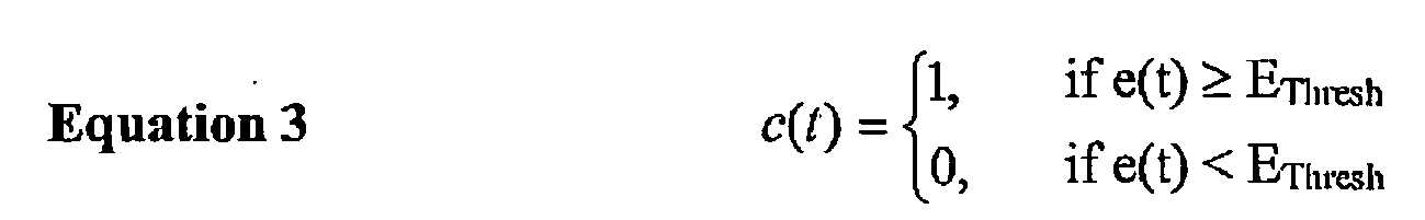
where EThresh is the signal envelope detector output value when the normalised signal amplitude is VOPT, It should be noted that the mathematical relation between EThresh and VOPT is dependent on the characteristics of the envelope detector.
- Hence EC will be a good measure for the wanted "tail area" ifN is made sufficiently large. The estimate for EC will in a practical implementation be extracted from the envelope of the RF signal. Feeding the envelope to a comparator and setting the reference to EThresh will give us the desired c(t). This two state signal (i.e. c(t) ) can then be sampled and accumulated according to Eq. 4. The solution to the imbalance problem is then reduced to the task of minimising EC with respect to (i), (ii) and (iii). This can be done by varying the three imbalance parameters and measure the corresponding change in EC. A possible process for this is shown in
Fig. 2 . An alternative process may be employed with the same detector solution, however, giving a different response pattern. The essential part, though, is to use the detector output information in a valid manner. - The approach suggested above counts occurrences of amplitudes above a certain level.An equivalent method would be to count occurences below a certain level, but then the count should be maximised instead of minimised. This is a special case of the more general solution where amplitude occurrences within one ore more intervals are counted. In a such solution we will need more than a 1-bit ADC (comparator) to realise
Equation 3. -
Fig. 1 shows a simplified block diagram of a quadrature modulator with an exemplary embodyment of the invention. - I- and Q-data are entering the block with
reference number 20. This block performs a traditional quadrature adjustment by adding controlled cross talk of I onto Q and vice versa. Thereafter I- and Q-channel gain are scaled by a factor with opposite sign for I-and Q-channel. The magnitude of both quadrature and gain adjustment are output from 10. I- and Q-data are further passed on to D/A converters 60 and the ordinary unwanted images from the conversion process are filtered in 80 before the signal is converted to RF or IF in 100. The conversion stage is done in quadrature, meaning that the local oscillator signal from 90 is phase shifted in 110 so that the LO feeding the Q-channel mixer is 90° out of phase with respect to the LO feeding the I-channel mixer. A diode-baseddetector 130 will give us a squared estimate of the envelope, but as long as the response is monotonic this satisfies our needs. The output from 130 is split and one part led to acomparator 120. Here the envelope is compared to a configurable threshold from 55. This threshold can be thought of as a trigger on the envelope: If the instantaneous envelope value is above the trigger, a logical 1 is the output from 120, otherwise a logical 0 is the output. This comparator value is sampled and accumulated in the digital domain in 30 according to Equation 4. After each NT second the adaptive process forimbalance correction 10 receives a new estimate for EC and outputs an adjustment.Block 10 has four outputs for adjustment of imbalance according to (i),(ii) and (iii), where the LO leakage occupies two of the outputs. DC_I and DC_Q are converted to analogue DC voltages at the output of 50 and applied as DC correction voltages at the input stage of 100. - The other branch from the
envelope detector 130 is low pass filtered in 140 and so that the mean value of the RF signal is extracted and sampled in 70. This information is required in order to ensure that the EThresh parameter approximately follows gain variations of the IF/RF signal. The EThresh is continuously adjusted in the EnvelopeThreshold Compensation block 40. Denote the output from 70 as EMEAN. The output from 40 is in this case EThresh = A·EMEAN + C , where A and C are configurable parameters. The inventors have found that good correspondence with Vopt is achieved by setting the value of A to about 4 dB. The optimum setting of A and C is reached when a gain difference at IF/RF has minimum impact on the estimate for EC. - The flow diagram here described may be associated to
Fig. 1 byblock 10. Each of the four parameter outputs from 10 have three associated properties: - 1. ParValue(k), stores the current value for each parameter.
- 2. Stepsize(k), holds the amount of change when adjusting the parameter
- 3. Direction(k), defines the current direction for next adjustment of the parameter.
+1 indicates increased next adjustment of ParValue(k), while -1 indicates decreased next adjustment of ParValue(k). - In 11 the properties are initialised and the parameter selector k is set to 0. The four possible values of k are to be interpreted as:
- k=0 :
- DC_I is the current parameter
- k=1 :
- DC_Q is the current parameter
- k=2 :
- Quad_adj is the current parameter
- k=3 :
- Gain_adj is the current parameter
- In 12 a new parameter value is computed and applied to the hardware. Then the accumulate time window counter ATW is started in 13 to keep track of the configurable integration time. The
next step 14 samples and accumulates the comparator output according to Equation 4. The Env_Count variable is equivalent to Ec except for the lack of normalisation. This accumulation is performed until the test inblock 15 indicates that the ATW counter has reached the integration time NT. A comparison of the current Env_count against the stored Env_count from last iteration is performed in 16. If the new estimate is greater than the old, we are obviously moving the parameter in the wrong direction and hence the direction property for this parameter is inverted in 17 so that the next time the parameter is tuned it will be in an opposite direction of the current one. In addition the adjustment of the parameter is temporarily stopped and the parameter selector k, increases by one, meaning that a different parameter will be tuned next time. k wraps around when it reaches 3. If the output from 15 is NO, the adjustment was successful and no change of direction or parameter is performed. The process ends up in 18 where the obtained estimate gets status as the old estimate. This means that the process has a memory of one envelope count estimate. The process then goes into an infinite loop back to 12. In this way we cycle through the four parameters and perform an independent adjustment of each. - The described system can be improved by introducing a enable/disable signal for the Env_Count accumulation variable. The idea is to enable counting only when the modulation trajectory corresponds to certain transmitted symbol sequences, e.g. selected corner points when detecting quadrature error.
- In addition, reduced variance of the adjustment parameter is obtained by defining ΔEnv_count = Env_count-Env_Count_Old. This delta information can be used to define a variable step size for the parameters. Another way to improve the variance is to have larger memory on the Env_Count variable.
- The main principles of this invention could also be adopted by a demodulator, suffering from the same deficiencies as the described modulator.
Claims (4)
- A method for optimising the performance of a vector modulation system arranged to output a complex signal, characterized in that said method comprises the steps of:measuring (30, 120) an area under a tail of an amplitude probability density curve of said complex signal, wherein the tail is defined by amplitudes above the highest expected value of the point of intersection where the amplitude probability density curve generated in absence of modulation impairment intersects an amplitude probability distribution curve generated in the presence of modulation impairment, and adjusting (20) at least one modulation impairment factor in order to minimize said area.
- The method of claim 1, wherein said modulation impairment factor is an LO carrier leakage, an I/Q orthogonality error or an I/Q gain imbalance.
- An arrangement for optimising the performance of a vector modulation system arranged to output a complex signal, characterized in that said arrangement comprises means (30, 120) for measuring an area under a tail of an amplitude probability density curve of said complex signal, wherein the tail is defined by amplitudes above the highest expected value of the point of intersection where the amplitude probability density curve generated in absence of modulation impairment intersects an amplitude probability distribution curve generated in the presence of modulation impairment, and means (20) for adjusting at least one modulation impairment factor in order to minimize said area.
- The arrangement of claim3, wherein said modulation impairment factor is an LO carrier leakage, an I/Q orthogonality error or an I/Q gain imbalance.
Applications Claiming Priority (2)
| Application Number | Priority Date | Filing Date | Title |
|---|---|---|---|
| NO20033695 | 2003-08-20 | ||
| NO20033695A NO321303B1 (en) | 2003-08-20 | 2003-08-20 | Adaptive imbalance correction in a quadrature modulator |
Publications (2)
| Publication Number | Publication Date |
|---|---|
| EP1511264A1 EP1511264A1 (en) | 2005-03-02 |
| EP1511264B1 true EP1511264B1 (en) | 2010-03-31 |
Family
ID=28036457
Family Applications (1)
| Application Number | Title | Priority Date | Filing Date |
|---|---|---|---|
| EP04019674A Expired - Lifetime EP1511264B1 (en) | 2003-08-20 | 2004-08-19 | Adaptive imbalance correction based on amplitude distribution |
Country Status (4)
| Country | Link |
|---|---|
| EP (1) | EP1511264B1 (en) |
| AT (1) | ATE463114T1 (en) |
| DE (1) | DE602004026255D1 (en) |
| NO (1) | NO321303B1 (en) |
Families Citing this family (2)
| Publication number | Priority date | Publication date | Assignee | Title |
|---|---|---|---|---|
| DE102005013881A1 (en) * | 2005-03-24 | 2006-09-28 | Infineon Technologies Ag | Signal processing method for portable radio involves amplifying carrier signal after amplitude of carrier signal is modulated based on distorted first component or first component |
| SE532400C2 (en) * | 2006-08-30 | 2010-01-12 | Nera Networks As | Method and apparatus for detecting and estimating quadrature defects |
Family Cites Families (3)
| Publication number | Priority date | Publication date | Assignee | Title |
|---|---|---|---|---|
| EP0324581A3 (en) * | 1988-01-13 | 1990-11-07 | Hewlett-Packard Company | Calibration of vector demodulator using statistical analysis |
| US5371481A (en) * | 1993-03-24 | 1994-12-06 | Nokia Mobile Phones Ltd. | Tuning techniques for I/Q channel signals in microwave digital transmission systems |
| JP2610092B2 (en) | 1993-03-25 | 1997-05-14 | 日本碍子株式会社 | Non-ceramic insulator metal fitting holding structure and metal fitting holding method |
-
2003
- 2003-08-20 NO NO20033695A patent/NO321303B1/en not_active IP Right Cessation
-
2004
- 2004-08-19 AT AT04019674T patent/ATE463114T1/en not_active IP Right Cessation
- 2004-08-19 EP EP04019674A patent/EP1511264B1/en not_active Expired - Lifetime
- 2004-08-19 DE DE602004026255T patent/DE602004026255D1/en not_active Expired - Lifetime
Also Published As
| Publication number | Publication date |
|---|---|
| ATE463114T1 (en) | 2010-04-15 |
| NO321303B1 (en) | 2006-04-24 |
| EP1511264A1 (en) | 2005-03-02 |
| NO20033695L (en) | 2005-02-21 |
| NO20033695D0 (en) | 2003-08-20 |
| DE602004026255D1 (en) | 2010-05-12 |
Similar Documents
| Publication | Publication Date | Title |
|---|---|---|
| US6785342B1 (en) | Nonlinear pre-distortion modulator and long loop control | |
| EP0617532B1 (en) | Calibration method for vector modulators | |
| US5113414A (en) | Predistortion arrangement for a digital transmission system | |
| CN1218475C (en) | Adaptive linearization of power amplifiers | |
| US6798844B2 (en) | Correction of phase and amplitude imbalance of I/Q modulator | |
| CN115250218B (en) | Broadband signal IQ imbalance and channel flatness calibration method | |
| WO1998024209A1 (en) | Method in digital quadrature modulator and demodulator, and digital quadrature modulator and demodulator | |
| CN1390393A (en) | Apparatus for interference compensation of a direct conversion transceiver and method | |
| US7248639B2 (en) | Method for reducing the out-of-band emission in AM transmitters for digital transmission | |
| WO2002089435A1 (en) | Controlled modulation distortion | |
| US20060050805A1 (en) | Method and apparatus for layered modulation | |
| US6535562B1 (en) | Method and apparatus for rotating the phase of a complex signal | |
| US4882547A (en) | Linearizer control system | |
| US20030157905A1 (en) | Transmitter and associated method for reducing the adjacent channel power during wireless communications | |
| Nash | Correcting imperfections in IQ modulators to improve RF signal fidelity | |
| US8027408B2 (en) | ASK modulator | |
| EP1511264B1 (en) | Adaptive imbalance correction based on amplitude distribution | |
| US6034573A (en) | Method and apparatus for calibrating modulation sensitivity | |
| US7142613B2 (en) | Methods, systems and devices for generating pulse shapes | |
| EP3297237A1 (en) | Method and system for generating an adapted transmission signal | |
| US20040109497A1 (en) | Communications system including a narrow band demodulator | |
| US6744827B1 (en) | Demodulator arrangement, method to demodulate, and telecommunication system comprising such a demodulator arrangement | |
| EP2547059B1 (en) | Transmitter including calibration of an in-phase/Quadrature (I/Q) modulator and associated methods | |
| KR20050030602A (en) | Method and circuit arrangement for deciding a symbol in the complex phase space of a quadrature modulation method | |
| JPH0568060A (en) | Distortion compensation quadrature modulator |
Legal Events
| Date | Code | Title | Description |
|---|---|---|---|
| PUAI | Public reference made under article 153(3) epc to a published international application that has entered the european phase |
Free format text: ORIGINAL CODE: 0009012 |
|
| 17P | Request for examination filed |
Effective date: 20040819 |
|
| AK | Designated contracting states |
Kind code of ref document: A1 Designated state(s): AT BE BG CH CY CZ DE DK EE ES FI FR GB GR HU IE IT LI LU MC NL PL PT RO SE SI SK TR |
|
| AX | Request for extension of the european patent |
Extension state: AL HR LT LV MK |
|
| AKX | Designation fees paid |
Designated state(s): AT BE BG CH CY CZ DE DK EE ES FI FR GB GR HU IE IT LI LU MC NL PL PT RO SE SI SK TR |
|
| 17Q | First examination report despatched |
Effective date: 20070510 |
|
| GRAP | Despatch of communication of intention to grant a patent |
Free format text: ORIGINAL CODE: EPIDOSNIGR1 |
|
| RAP1 | Party data changed (applicant data changed or rights of an application transferred) |
Owner name: NERA NETWORKS AS |
|
| GRAS | Grant fee paid |
Free format text: ORIGINAL CODE: EPIDOSNIGR3 |
|
| GRAA | (expected) grant |
Free format text: ORIGINAL CODE: 0009210 |
|
| AK | Designated contracting states |
Kind code of ref document: B1 Designated state(s): AT BE BG CH CY CZ DE DK EE ES FI FR GB GR HU IE IT LI LU MC NL PL PT RO SE SI SK TR |
|
| REG | Reference to a national code |
Ref country code: GB Ref legal event code: FG4D Ref country code: CH Ref legal event code: EP |
|
| REG | Reference to a national code |
Ref country code: IE Ref legal event code: FG4D |
|
| REF | Corresponds to: |
Ref document number: 602004026255 Country of ref document: DE Date of ref document: 20100512 Kind code of ref document: P |
|
| REG | Reference to a national code |
Ref country code: NL Ref legal event code: VDEP Effective date: 20100331 |
|
| PG25 | Lapsed in a contracting state [announced via postgrant information from national office to epo] |
Ref country code: SI Free format text: LAPSE BECAUSE OF FAILURE TO SUBMIT A TRANSLATION OF THE DESCRIPTION OR TO PAY THE FEE WITHIN THE PRESCRIBED TIME-LIMIT Effective date: 20100331 Ref country code: AT Free format text: LAPSE BECAUSE OF FAILURE TO SUBMIT A TRANSLATION OF THE DESCRIPTION OR TO PAY THE FEE WITHIN THE PRESCRIBED TIME-LIMIT Effective date: 20100331 Ref country code: FI Free format text: LAPSE BECAUSE OF FAILURE TO SUBMIT A TRANSLATION OF THE DESCRIPTION OR TO PAY THE FEE WITHIN THE PRESCRIBED TIME-LIMIT Effective date: 20100331 Ref country code: PL Free format text: LAPSE BECAUSE OF FAILURE TO SUBMIT A TRANSLATION OF THE DESCRIPTION OR TO PAY THE FEE WITHIN THE PRESCRIBED TIME-LIMIT Effective date: 20100331 |
|
| PG25 | Lapsed in a contracting state [announced via postgrant information from national office to epo] |
Ref country code: RO Free format text: LAPSE BECAUSE OF FAILURE TO SUBMIT A TRANSLATION OF THE DESCRIPTION OR TO PAY THE FEE WITHIN THE PRESCRIBED TIME-LIMIT Effective date: 20100331 Ref country code: NL Free format text: LAPSE BECAUSE OF FAILURE TO SUBMIT A TRANSLATION OF THE DESCRIPTION OR TO PAY THE FEE WITHIN THE PRESCRIBED TIME-LIMIT Effective date: 20100331 Ref country code: ES Free format text: LAPSE BECAUSE OF FAILURE TO SUBMIT A TRANSLATION OF THE DESCRIPTION OR TO PAY THE FEE WITHIN THE PRESCRIBED TIME-LIMIT Effective date: 20100712 Ref country code: EE Free format text: LAPSE BECAUSE OF FAILURE TO SUBMIT A TRANSLATION OF THE DESCRIPTION OR TO PAY THE FEE WITHIN THE PRESCRIBED TIME-LIMIT Effective date: 20100331 Ref country code: BE Free format text: LAPSE BECAUSE OF FAILURE TO SUBMIT A TRANSLATION OF THE DESCRIPTION OR TO PAY THE FEE WITHIN THE PRESCRIBED TIME-LIMIT Effective date: 20100331 Ref country code: CY Free format text: LAPSE BECAUSE OF FAILURE TO SUBMIT A TRANSLATION OF THE DESCRIPTION OR TO PAY THE FEE WITHIN THE PRESCRIBED TIME-LIMIT Effective date: 20100331 Ref country code: SE Free format text: LAPSE BECAUSE OF FAILURE TO SUBMIT A TRANSLATION OF THE DESCRIPTION OR TO PAY THE FEE WITHIN THE PRESCRIBED TIME-LIMIT Effective date: 20100331 |
|
| PG25 | Lapsed in a contracting state [announced via postgrant information from national office to epo] |
Ref country code: CZ Free format text: LAPSE BECAUSE OF FAILURE TO SUBMIT A TRANSLATION OF THE DESCRIPTION OR TO PAY THE FEE WITHIN THE PRESCRIBED TIME-LIMIT Effective date: 20100331 Ref country code: SK Free format text: LAPSE BECAUSE OF FAILURE TO SUBMIT A TRANSLATION OF THE DESCRIPTION OR TO PAY THE FEE WITHIN THE PRESCRIBED TIME-LIMIT Effective date: 20100331 |
|
| PG25 | Lapsed in a contracting state [announced via postgrant information from national office to epo] |
Ref country code: DK Free format text: LAPSE BECAUSE OF FAILURE TO SUBMIT A TRANSLATION OF THE DESCRIPTION OR TO PAY THE FEE WITHIN THE PRESCRIBED TIME-LIMIT Effective date: 20100331 Ref country code: PT Free format text: LAPSE BECAUSE OF FAILURE TO SUBMIT A TRANSLATION OF THE DESCRIPTION OR TO PAY THE FEE WITHIN THE PRESCRIBED TIME-LIMIT Effective date: 20100802 |
|
| PLBE | No opposition filed within time limit |
Free format text: ORIGINAL CODE: 0009261 |
|
| STAA | Information on the status of an ep patent application or granted ep patent |
Free format text: STATUS: NO OPPOSITION FILED WITHIN TIME LIMIT |
|
| 26N | No opposition filed |
Effective date: 20110104 |
|
| PG25 | Lapsed in a contracting state [announced via postgrant information from national office to epo] |
Ref country code: MC Free format text: LAPSE BECAUSE OF NON-PAYMENT OF DUE FEES Effective date: 20100831 Ref country code: IT Free format text: LAPSE BECAUSE OF FAILURE TO SUBMIT A TRANSLATION OF THE DESCRIPTION OR TO PAY THE FEE WITHIN THE PRESCRIBED TIME-LIMIT Effective date: 20100331 |
|
| REG | Reference to a national code |
Ref country code: CH Ref legal event code: PL |
|
| PG25 | Lapsed in a contracting state [announced via postgrant information from national office to epo] |
Ref country code: CH Free format text: LAPSE BECAUSE OF NON-PAYMENT OF DUE FEES Effective date: 20100831 Ref country code: LI Free format text: LAPSE BECAUSE OF NON-PAYMENT OF DUE FEES Effective date: 20100831 |
|
| REG | Reference to a national code |
Ref country code: FR Ref legal event code: ST Effective date: 20110502 |
|
| REG | Reference to a national code |
Ref country code: DE Ref legal event code: R119 Ref document number: 602004026255 Country of ref document: DE Effective date: 20110301 |
|
| PG25 | Lapsed in a contracting state [announced via postgrant information from national office to epo] |
Ref country code: IE Free format text: LAPSE BECAUSE OF NON-PAYMENT OF DUE FEES Effective date: 20100819 Ref country code: DE Free format text: LAPSE BECAUSE OF NON-PAYMENT OF DUE FEES Effective date: 20110301 Ref country code: FR Free format text: LAPSE BECAUSE OF NON-PAYMENT OF DUE FEES Effective date: 20100831 |
|
| PG25 | Lapsed in a contracting state [announced via postgrant information from national office to epo] |
Ref country code: HU Free format text: LAPSE BECAUSE OF FAILURE TO SUBMIT A TRANSLATION OF THE DESCRIPTION OR TO PAY THE FEE WITHIN THE PRESCRIBED TIME-LIMIT Effective date: 20101001 Ref country code: BG Free format text: LAPSE BECAUSE OF FAILURE TO SUBMIT A TRANSLATION OF THE DESCRIPTION OR TO PAY THE FEE WITHIN THE PRESCRIBED TIME-LIMIT Effective date: 20100331 Ref country code: LU Free format text: LAPSE BECAUSE OF NON-PAYMENT OF DUE FEES Effective date: 20100819 |
|
| PG25 | Lapsed in a contracting state [announced via postgrant information from national office to epo] |
Ref country code: TR Free format text: LAPSE BECAUSE OF FAILURE TO SUBMIT A TRANSLATION OF THE DESCRIPTION OR TO PAY THE FEE WITHIN THE PRESCRIBED TIME-LIMIT Effective date: 20100331 |
|
| PGFP | Annual fee paid to national office [announced via postgrant information from national office to epo] |
Ref country code: GB Payment date: 20120815 Year of fee payment: 9 |
|
| PG25 | Lapsed in a contracting state [announced via postgrant information from national office to epo] |
Ref country code: BG Free format text: LAPSE BECAUSE OF FAILURE TO SUBMIT A TRANSLATION OF THE DESCRIPTION OR TO PAY THE FEE WITHIN THE PRESCRIBED TIME-LIMIT Effective date: 20100630 |
|
| GBPC | Gb: european patent ceased through non-payment of renewal fee |
Effective date: 20130819 |
|
| PG25 | Lapsed in a contracting state [announced via postgrant information from national office to epo] |
Ref country code: GB Free format text: LAPSE BECAUSE OF NON-PAYMENT OF DUE FEES Effective date: 20130819 |
|
| PG25 | Lapsed in a contracting state [announced via postgrant information from national office to epo] |
Ref country code: GR Free format text: LAPSE BECAUSE OF FAILURE TO SUBMIT A TRANSLATION OF THE DESCRIPTION OR TO PAY THE FEE WITHIN THE PRESCRIBED TIME-LIMIT Effective date: 20100331 |