EP0617532A1 - Calibration method for vector modulators - Google Patents
Calibration method for vector modulators Download PDFInfo
- Publication number
- EP0617532A1 EP0617532A1 EP94302041A EP94302041A EP0617532A1 EP 0617532 A1 EP0617532 A1 EP 0617532A1 EP 94302041 A EP94302041 A EP 94302041A EP 94302041 A EP94302041 A EP 94302041A EP 0617532 A1 EP0617532 A1 EP 0617532A1
- Authority
- EP
- European Patent Office
- Prior art keywords
- signal
- amplitude
- phase
- power
- component
- Prior art date
- Legal status (The legal status is an assumption and is not a legal conclusion. Google has not performed a legal analysis and makes no representation as to the accuracy of the status listed.)
- Granted
Links
- 239000013598 vector Substances 0.000 title claims abstract description 45
- 238000000034 method Methods 0.000 title abstract description 13
- 230000004044 response Effects 0.000 claims description 6
- 230000005055 memory storage Effects 0.000 claims 1
- 238000005259 measurement Methods 0.000 abstract description 10
- 238000012937 correction Methods 0.000 abstract description 9
- 230000015654 memory Effects 0.000 abstract description 3
- 230000010363 phase shift Effects 0.000 description 5
- 238000010586 diagram Methods 0.000 description 4
- 238000004519 manufacturing process Methods 0.000 description 4
- 238000012545 processing Methods 0.000 description 4
- 230000005540 biological transmission Effects 0.000 description 3
- 230000008901 benefit Effects 0.000 description 2
- 230000007704 transition Effects 0.000 description 2
- 230000032683 aging Effects 0.000 description 1
- 230000001668 ameliorated effect Effects 0.000 description 1
- 239000000969 carrier Substances 0.000 description 1
- 230000001413 cellular effect Effects 0.000 description 1
- 230000008859 change Effects 0.000 description 1
- 238000004891 communication Methods 0.000 description 1
- 230000000694 effects Effects 0.000 description 1
- 238000005516 engineering process Methods 0.000 description 1
- 230000006870 function Effects 0.000 description 1
- 238000013507 mapping Methods 0.000 description 1
- 230000008569 process Effects 0.000 description 1
- 238000007493 shaping process Methods 0.000 description 1
Images


Classifications
-
- H—ELECTRICITY
- H04—ELECTRIC COMMUNICATION TECHNIQUE
- H04L—TRANSMISSION OF DIGITAL INFORMATION, e.g. TELEGRAPHIC COMMUNICATION
- H04L27/00—Modulated-carrier systems
- H04L27/32—Carrier systems characterised by combinations of two or more of the types covered by groups H04L27/02, H04L27/10, H04L27/18 or H04L27/26
- H04L27/34—Amplitude- and phase-modulated carrier systems, e.g. quadrature-amplitude modulated carrier systems
- H04L27/36—Modulator circuits; Transmitter circuits
- H04L27/362—Modulation using more than one carrier, e.g. with quadrature carriers, separately amplitude modulated
- H04L27/364—Arrangements for overcoming imperfections in the modulator, e.g. quadrature error or unbalanced I and Q levels
-
- H—ELECTRICITY
- H03—ELECTRONIC CIRCUITRY
- H03C—MODULATION
- H03C3/00—Angle modulation
- H03C3/38—Angle modulation by converting amplitude modulation to angle modulation
- H03C3/40—Angle modulation by converting amplitude modulation to angle modulation using two signal paths the outputs of which have a predetermined phase difference and at least one output being amplitude-modulated
- H03C3/406—Angle modulation by converting amplitude modulation to angle modulation using two signal paths the outputs of which have a predetermined phase difference and at least one output being amplitude-modulated using a feedback loop containing mixers or demodulators
-
- H—ELECTRICITY
- H04—ELECTRIC COMMUNICATION TECHNIQUE
- H04B—TRANSMISSION
- H04B1/00—Details of transmission systems, not covered by a single one of groups H04B3/00 - H04B13/00; Details of transmission systems not characterised by the medium used for transmission
- H04B1/02—Transmitters
- H04B1/04—Circuits
- H04B1/0475—Circuits with means for limiting noise, interference or distortion
-
- H—ELECTRICITY
- H04—ELECTRIC COMMUNICATION TECHNIQUE
- H04L—TRANSMISSION OF DIGITAL INFORMATION, e.g. TELEGRAPHIC COMMUNICATION
- H04L27/00—Modulated-carrier systems
- H04L27/18—Phase-modulated carrier systems, i.e. using phase-shift keying
- H04L27/20—Modulator circuits; Transmitter circuits
- H04L27/2032—Modulator circuits; Transmitter circuits for discrete phase modulation, e.g. in which the phase of the carrier is modulated in a nominally instantaneous manner
- H04L27/2053—Modulator circuits; Transmitter circuits for discrete phase modulation, e.g. in which the phase of the carrier is modulated in a nominally instantaneous manner using more than one carrier, e.g. carriers with different phases
- H04L27/206—Modulator circuits; Transmitter circuits for discrete phase modulation, e.g. in which the phase of the carrier is modulated in a nominally instantaneous manner using more than one carrier, e.g. carriers with different phases using a pair of orthogonal carriers, e.g. quadrature carriers
- H04L27/2067—Modulator circuits; Transmitter circuits for discrete phase modulation, e.g. in which the phase of the carrier is modulated in a nominally instantaneous manner using more than one carrier, e.g. carriers with different phases using a pair of orthogonal carriers, e.g. quadrature carriers with more than two phase states
- H04L27/2071—Modulator circuits; Transmitter circuits for discrete phase modulation, e.g. in which the phase of the carrier is modulated in a nominally instantaneous manner using more than one carrier, e.g. carriers with different phases using a pair of orthogonal carriers, e.g. quadrature carriers with more than two phase states in which the data are represented by the carrier phase, e.g. systems with differential coding
Definitions
- the present invention relates to vector modulation systems, and more particularly to vector modulation systems including I/Q modulators and tuning techniques therefor.
- RF or Microwave communications using digital modulation techniques require signal modulators which perform vector or quadrature modulation.
- two modulation input signals independently modulate the in-phase (I) and quadrature (Q) components of the carrier.
- the I and Q channels of the modulator must be calibrated to be equal in gain, i.e., balanced, and precisely 90° apart, i.e., in quadrature.
- One way to calibrate a vector modulator is with a network analyzer connected to the RF carrier input and to the RF modulated output.
- the network analyzer measures the amplitude and phase of the RF modulated output resulting from varying DC voltages applied to the I and Q modulation inputs. From these measurements, the gain and phase accuracy of the modulator can be determined, and calibrated. This is an expensive and complicated technique that is also limited in accuracy.
- Structure and techniques for calibrating a vector modulator that does not require a network analyzer are provided by the present invention and incorporated in a system comprising a standard vector modulator circuit including means for shifting phase to adjust the relative phases of the I and Q components of the modulated RF carrier. Means for variable attenuating are included in the I and Q modulation system to adjust the relative amplitude of the modulation signals.
- a vector modulation system comprising: I/Q encloder means for providing an I component signal for the in-phase I component of a data signal and a Q component signal for the quadrature Q component of the data signal, modulating means for modulating an in-phase I component of a carrier signal by the I component signal and for modulating a quadrature Q component of a carrier signal by the Q component signal, means for combining the I and Q modulated carrier signal components into a combined I and Q modualted carrier signal, measuring means for measuring the power of selected frequencies of the combined and Q modulated carrier signal and to determine differences between phase of the modulated I and Q carrier signal components, means responsive to the power measuring means for generating a respective amplitude compensation signal and phase compensation signal corresponding to the differences between the amplitude and phase of the I and Q modulated carrier signal components, and, means for providing a difference reducation signal derived from the respective amplitude compensation signal and phase compensation signal to the I/Q encoder means to reduce the amplitude and phase differnces
- a vector modulator in accordance with the invention may compensate for differences between amplitude and phase by signal processing, in particular it would be possible to use digital signal processing.
- the difference or error compensation is achieved by first determining amplitude error or unbalance by I and Q signal power measurement and an amplitude compensation signal is stored, then a power measurement is carried out for phase compensation and a phase compensation signal is stored.
- the amplitude and phase compensation signals are used to modify the I/Q digital input signals.
- Such a vector modulator has correction signals generated by measuring the power of the modulator output signal and comparing them to stored correction values.
- no external calibration circuitry is required, which eases manufacture and reduces cost.
- recalibration may be performed after manufacture.
- Fig. 1 shows a vector modulator in accordance with the present invention.
- a vector modulator sometimes referred to as an I/Q modulator, is employed in microwave transmitters such as used in cellular telephones.
- a vector modulator applies two separate modulation signals to modulate the in-phase (I) and quadrature (Q) components of a carrier signal.
- a typical system used in the art is designated 10 in Fig. 1 and includes an I/Q encoder 12 that generates a first (I) digital signal on lead 14 and a second (Q) digital signal on lead 16.
- the I digital signal on lead 14 is converted to an analog signal by digital-to-analog converter (DAC) 18 and the analog signal is smoothed by baseband filter 20.
- the Q digital signal on lead 16 is changed to an analog signal at digital-to-analog converter (DAC) 22 and smoothed at baseband filter means 24.
- DAC digital-to-analog converter
- An RF carrier signal is generated by local oscillator 26 and is divided by a 90 degree power divider means 28 to provide an in-phase I signal component on lead 30 and a +90 degree quadrature Q signal component on lead 32.
- the analog I component signal from filter 20 on lead 34 modulates the I component of the carrier signal on lead 30 at multiplier 36.
- the analog Q component signal on lead 38 modulates the Q component of the carrier signal from filter 24 on lead 32 at multiplier 40.
- the modulated I and Q carrier signals on leads 42 and 44 are combined by a 0 degree power combiner 46 to produce the vector modulated RF output signal that is transmitted via antenna 48 after being passed through a power control unit 50.
- the output power of selected frequencies of the RF output signal at antenna 48 are measured by a narrow band power meter 52.
- the outputs of the narrow band power meter 52 which will be more fully described and explained, are applied to a measurement processor 54 which calculates the desired corrections to any amplitude and phase errors of the I and Q signals and transmits a correction signal to the I/Q coder 12 to calibrate or tune the modulator system.
- Amplitude balance of a quadrature or vector modulator used in digital mobile phone technology can be achieved by tuning.
- tuning is carried out by the use of a trimmer resistor.
- the tuning is done by using digital techniques.
- the I and Q signals used in vector modulators are digital signals generated by coding circuits and the amplitude of the signals can therefore effectively be tuned by digital correction signals.
- both the gain and the difference of the I and Q branches due to DACs, filters, mixers, and summer can be compensated for, and amplitude differences of quadrature carriers caused by temperature changes can also be corrected.
- the amplitude tuning values can be stored in memory circuits such as electrically erasable programmable read-only memories (EEPROMs).
- EEPROMs electrically erasable programmable read-only memories
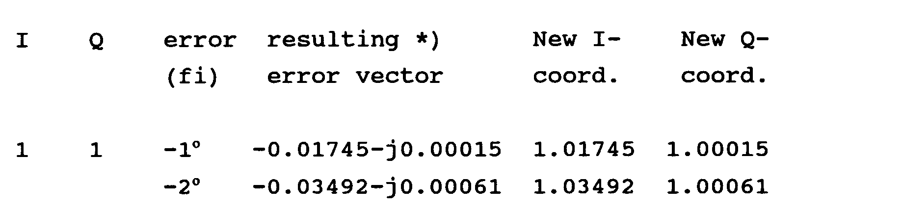
- the tuning process for the error compensation initially includes measuring the power levels of the I signal component and the Q signal component with the default I/Q coordinates (0,+-1, +- ⁇ 2). Then a correction term is summed to the I- and Q-coordinates so that resulting vector, despite the phase error, is correct.
- the phase error (90 degrees minus the actual phase between the I and Q components is increased in steps of one degree so the error vectors will be, for example, as follows: ..and so on.
- the power level measurement information from narrow band power meter 52 is transmitted via a data bus to the data processor 54.
- the vector modulation section 10 employs known prior art encoding and vector modulation techniques and transmitter voice-signal processing stages.
- the voice encoded I and Q signal components consisting of zero to one and one to zero transitions are applied to the respective digital to analog converters (DACs) 18 and 22 to produce wide band analog signals which are applied to base band filters 20 and 24, the outputs of which are used to modulate the I and Q components of the carrier signal on leads 30 and 32.
- DACs digital to analog converters
- the modulation method used is known in the art as ⁇ /4 shifted differentialy encoded quadrature phase shift keying.
- the modulation of the carrier consists of a cosine component and a sine component.
- the cosine component of the signal vector is the in-phase or I signal and the sine component of the signal vector is the quadrature, or Q signal.
- the I and Q signal vector components are mixed with the I and Q components of the carrier signal and summed to create the transmission signal.
- Signals representing the vector components I and Q of the phase shift of the signal vector are generated by shifting the signal vector such that phase shifts of the carrier of ⁇ 3 ⁇ /4 radians are generated.
- Each phase shift (-3 ⁇ /4, +3 ⁇ /4, + ⁇ /4, - ⁇ /4) encodes one of four possible signals.
- the modulation scheme uses the phase constellation shown in Figure 3. Note that Gray code is used in the mapping: two di-bit symbols corresponding to adjacent signal phases differ only in a single bit. Since most probable errors due to noise result in the erroneous selection of an adjacent phase, most di-bit symbol errors contain only a single bit error.
- FIG. 4 A block diagram of the differential encoder is shown in Figure 4.
- the binary data stream entering the modulator b m is converted by a serial-to-parallel converter into two separate binary streams (X k ) and (Y k ). Starting from bit 1 in time of stream b m , all odd numbered bits form stream X k and all even numbered bits form stream Y k .
- the phase change ⁇ is determined according to the following table: X k Y k ⁇ 1 1 -3 ⁇ /4 0 1 3 ⁇ /4 0 0 - ⁇ /4 1 0 - ⁇ /4
- the signals I k ,Q k at the output of the differential phase encoding means in Fig. 4 can take one of five values. O, ⁇ 1, ⁇ 1/ ⁇ 2, resulting in the constellation shown in Figure 3.
- Pulses I k , Q k from the I/Q coder 12 of Fig. 1 are converted to analog signals by DACs 18 and 22 and are applied to the inputs of the I & Q base-band filters 20 and 24.
- the base-band filters have linear phase and square root raised cosine frequency response of the form: where T is the symbol period.
- the roll-off factor, a determines the width of the transition band.
- g(t) is the pulse shaping function
- W c is the radian carrier frequency
- T is the symbol period
- ⁇ n is the absolute phase corresponding to the n th symbol interval.
- ⁇ n ⁇ n-1 + ⁇ n .
- Any method which generates the specified s(t) using the cited phase table may be used.
- the output power can also be tuned by amplitudes of I and Q signals. This can be necessaryy when the power control window is too narrow.
- the position of the power control window is tuned by I and Q amplitudes. This tuning compensates the variations of the position of the power control window caused by the tolerances of the components.
- the output power can be tuned by I and Q amplitudes.
- phase error can be compensated by digital signal processing and the modulator is tuned by stored computed values.
- the correction signals for the phase error is determined by measuring the power level from the modulator output.
Landscapes
- Engineering & Computer Science (AREA)
- Computer Networks & Wireless Communication (AREA)
- Signal Processing (AREA)
- Digital Transmission Methods That Use Modulated Carrier Waves (AREA)
Abstract
Description
- The present invention relates to vector modulation systems, and more particularly to vector modulation systems including I/Q modulators and tuning techniques therefor.
- RF or Microwave communications using digital modulation techniques require signal modulators which perform vector or quadrature modulation. In vector modulation two modulation input signals independently modulate the in-phase (I) and quadrature (Q) components of the carrier. For proper operation, the I and Q channels of the modulator must be calibrated to be equal in gain, i.e., balanced, and precisely 90° apart, i.e., in quadrature.
- One way to calibrate a vector modulator is with a network analyzer connected to the RF carrier input and to the RF modulated output. The network analyzer measures the amplitude and phase of the RF modulated output resulting from varying DC voltages applied to the I and Q modulation inputs. From these measurements, the gain and phase accuracy of the modulator can be determined, and calibrated. This is an expensive and complicated technique that is also limited in accuracy. Structure and techniques for calibrating a vector modulator that does not require a network analyzer, are provided by the present invention and incorporated in a system comprising a standard vector modulator circuit including means for shifting phase to adjust the relative phases of the I and Q components of the modulated RF carrier. Means for variable attenuating are included in the I and Q modulation system to adjust the relative amplitude of the modulation signals.
- According to the present invention there is provided a vector modulation system comprising:
I/Q encloder means for providing an I component signal for the in-phase I component of a data signal and a Q component signal for the quadrature Q component of the data signal, modulating means for modulating an in-phase I component of a carrier signal by the I component signal and for modulating a quadrature Q component of a carrier signal by the Q component signal,
means for combining the I and Q modulated carrier signal components into a combined I and Q modualted carrier signal,
measuring means for measuring the power of selected frequencies of the combined and Q modulated carrier signal and to determine differences between phase of the modulated I and Q carrier signal components,
means responsive to the power measuring means for generating a respective amplitude compensation signal and phase compensation signal corresponding to the differences between the amplitude and phase of the I and Q modulated carrier signal components, and,
means for providing a difference reducation signal derived from the respective amplitude compensation signal and phase compensation signal to the I/Q encoder means to reduce the amplitude and phase differnces. of the I and Q modulated carrier signal components. - This has the advantage that a vector modulator in accordance with the invention may compensate for differences between amplitude and phase by signal processing, in particular it would be possible to use digital signal processing.
- More particularly, the difference or error compensation is achieved by first determining amplitude error or unbalance by I and Q signal power measurement and an amplitude compensation signal is stored, then a power measurement is carried out for phase compensation and a phase compensation signal is stored. The amplitude and phase compensation signals are used to modify the I/Q digital input signals.
- This has the advantage that such a vector modulator is an improved vector modulator wherein the modulator is tuned by stored computed correction values.
- Additionally such a vector modulator has correction signals generated by measuring the power of the modulator output signal and comparing them to stored correction values. Thus, no external calibration circuitry is required, which eases manufacture and reduces cost. Furthermore, recalibration may be performed after manufacture.
- A description of a preferred embodiment will now be given by way of example only and with reference to the accompanying drawings in which:
- Fig. 1 is a schematic block diagram illustrating a vector modulator system including phase compensation in accordance with the present invention;
- Fig. 2 is a diagram illustrating the effect of phase error on the I and Q signal components of the vector modulator;
- Fig. 3 is an illustration of a phase constellation used in this explanation of the present invention; and
- Fig. 4 is a schematic block diagram of a differential encoder employed in the embodiment of the present invention.
- Fig. 1 shows a vector modulator in accordance with the present invention. A vector modulator, sometimes referred to as an I/Q modulator, is employed in microwave transmitters such as used in cellular telephones. A vector modulator applies two separate modulation signals to modulate the in-phase (I) and quadrature (Q) components of a carrier signal. A typical system used in the art is designated 10 in Fig. 1 and includes an I/
Q encoder 12 that generates a first (I) digital signal onlead 14 and a second (Q) digital signal onlead 16. The I digital signal onlead 14 is converted to an analog signal by digital-to-analog converter (DAC) 18 and the analog signal is smoothed bybaseband filter 20. Likewise, the Q digital signal onlead 16 is changed to an analog signal at digital-to-analog converter (DAC) 22 and smoothed at baseband filter means 24. - An RF carrier signal is generated by
local oscillator 26 and is divided by a 90 degree power divider means 28 to provide an in-phase I signal component onlead 30 and a +90 degree quadrature Q signal component onlead 32. - The analog I component signal from
filter 20 onlead 34 modulates the I component of the carrier signal onlead 30 atmultiplier 36. Likewise, the analog Q component signal onlead 38 modulates the Q component of the carrier signal fromfilter 24 onlead 32 atmultiplier 40. The modulated I and Q carrier signals onleads antenna 48 after being passed through apower control unit 50. - As previously stated, the I/Q modulator as before described is known and documented in the art.
- In accordance with the present invention, the output power of selected frequencies of the RF output signal at
antenna 48 are measured by a narrowband power meter 52. The outputs of the narrowband power meter 52, which will be more fully described and explained, are applied to ameasurement processor 54 which calculates the desired corrections to any amplitude and phase errors of the I and Q signals and transmits a correction signal to the I/Q coder 12 to calibrate or tune the modulator system. - Amplitude balance of a quadrature or vector modulator used in digital mobile phone technology can be achieved by tuning. Conventionally in the prior art, tuning is carried out by the use of a trimmer resistor. In accordance with the present invention the tuning is done by using digital techniques. The I and Q signals used in vector modulators are digital signals generated by coding circuits and the amplitude of the signals can therefore effectively be tuned by digital correction signals.
- By utilising apparatus in accordance with the present invention both the gain and the difference of the I and Q branches due to DACs, filters, mixers, and summer can be compensated for, and amplitude differences of quadrature carriers caused by temperature changes can also be corrected.
- The amplitude tuning values can be stored in memory circuits such as electrically erasable programmable read-only memories (EEPROMs).
- The tuning process for the error compensation initially includes measuring the power levels of the I signal component and the Q signal component with the default I/Q coordinates (0,+-1, +-√2). Then a correction term is summed to the I- and Q-coordinates so that resulting vector, despite the phase error, is correct. The phase error (90 degrees minus the actual phase between the I and Q components is increased in steps of one degree so the error vectors will be, for example, as follows:

..and so on. - If the power level difference becomes smaller, the direction of the phase error is in the other direction and the previous example would now be:
- The power level measurement information from narrow
band power meter 52 is transmitted via a data bus to thedata processor 54. - In the system shown in Fig. 1, the vector modulation section 10 employs known prior art encoding and vector modulation techniques and transmitter voice-signal processing stages. The voice encoded I and Q signal components, consisting of zero to one and one to zero transitions are applied to the respective digital to analog converters (DACs) 18 and 22 to produce wide band analog signals which are applied to
base band filters leads - The modulation method used is known in the art as π/4 shifted differentialy encoded quadrature phase shift keying.
- In the π/4 shift differential quadrature phase shift keying technique, the modulation of the carrier consists of a cosine component and a sine component. The cosine component of the signal vector is the in-phase or I signal and the sine component of the signal vector is the quadrature, or Q signal.
- The I and Q signal vector components are mixed with the I and Q components of the carrier signal and summed to create the transmission signal. Signals representing the vector components I and Q of the phase shift of the signal vector are generated by shifting the signal vector such that phase shifts of the carrier of ±3π/4 radians are generated. Each phase shift (-3π/4, +3π/4, + π/4, -π/4) encodes one of four possible signals.
- The modulation scheme uses the phase constellation shown in Figure 3. Note that Gray code is used in the mapping: two di-bit symbols corresponding to adjacent signal phases differ only in a single bit. Since most probable errors due to noise result in the erroneous selection of an adjacent phase, most di-bit symbol errors contain only a single bit error.
- Note also, the rotation by π/4 of the basic QPSK constellation for odd (denoted ⊕) and even (denoted ⊗) symbols.
- In π/4 modulation the information is differentially encoded, that is, the symbols are transmitted as changes in phase rather than absolute phases. A block diagram of the differential encoder is shown in Figure 4. The binary data stream entering the modulator bm, is converted by a serial-to-parallel converter into two separate binary streams (Xk) and (Yk). Starting from
bit 1 in time of stream bm, all odd numbered bits form stream Xk and all even numbered bits form stream Yk. - The digital data sequences (Xk) and (Yk) are encoded onto (Ik) and (Qk) according to:


where Ik and Qk-1 are the amplitudes at the previous pulse time and k is an index of the bit pairs. The phase change Δφ is determined according to the following table:Xk Yk Δφ 1 1 -3π/4 0 1 3π/4 0 0 -π/4 1 0 -π/4 - The signals Ik,Qk at the output of the differential phase encoding means in Fig. 4 can take one of five values. O, ± 1, ± 1/√2, resulting in the constellation shown in Figure 3.
- Pulses Ik, Qk from the I/
Q coder 12 of Fig. 1 are converted to analog signals byDACs band filters 
where T is the symbol period. The roll-off factor, a, determines the width of the transition band. - The resultant transmitted signal s(t) from
power combiner 46 in Fig. 1 is given by:
where g(t) is the pulse shaping function, Wc is the radian carrier frequency. T is the symbol period, and φn is the absolute phase corresponding to the nth symbol interval. - The φn which results from the differential encoding is:

- Any method which generates the specified s(t) using the cited phase table may be used.
- The sequence of operations for a typical example of I/Q tuning in accordance with the present invention is as follows:
- 1. Initial transmitter settings
- mode: digital
- channel 300 (Fo=834 MHz)
- TX power level O
- set AFC to the previously tuned analog AFC value
- value for phase compensation is loaded in the processor in the beginning
- value for amplitude compensation is loaded in the processor in the beginning
- value for amplitude level is loaded in the processor in the beginning
- continuous transmission on
- modulating symbols 1-chain
- 2. Measuring:
- measure the narrow band RF-power using 2.5 kHz filter power meter on antenna connector - 3. Local Sequence:
- Modulator Tuning
- provide compensation values for:
- amplitude level
- amplitude compensation
- phase compensation
- Continuous Transmission
- 4. Adjustment
- 1. Set Scale factor (36.0 dBm)
- 2. Amplitude
- Measure the power levels on the carrier frequency of Fo-9.1125 kHz and Fo+9.1125 kHz. Compare the levels. SSB attenuation (level difference) should be as big as possible, so that Fo-9.1125 kHz level is higher. Adjust and load amplitude compensation value and repeat measurement. This is repeated till maximum SSB-attenuation has been achieved. Store value to EEPROM in meaurement processor.
- Measure SSB attenuation as described in 2. Adjust and load new value for phase compensation and repeat measurements on the two mentioned frequencies. The phase compensation value will be adjusted till maximum SSB attenuation has been achieved. After these two compensations SSB-attenuation must be > 32 dB. Store value to EEPROM in the measurement processor.
- Decrease/load amplitude level value to transmitter unit and measure RF-power (BW > 30 kHz). This is repeated till RF-power drops 0.5 dB (35.5dBm) below 36.0 dBm.
- When this level has been achieved, increase both compensation values (I & Q) with a multiplier, which corresponds 1.5 dB increase in ITX and QTX signal amplitudes. Store scale factor to EEPROM.
- As an extension of the normal power control of the transmitter the output power can also be tuned by amplitudes of I and Q signals. This can be necesary when the power control window is too narrow.
- Because of tolerances of components and variations of temperature, the power control could run out in high end or low end of output power. This problem can be ameliorated using the present invention.
- In production the position of the power control window is tuned by I and Q amplitudes. This tuning compensates the variations of the position of the power control window caused by the tolerances of the components.
- After production tuning when the system is in use in a mobile phone, if the TX power control runs out caused by temperature or aging, the output power can be tuned by I and Q amplitudes.
- What has been described is an improved vector modulator wherein phase error can be compensated by digital signal processing and the modulator is tuned by stored computed values. The correction signals for the phase error is determined by measuring the power level from the modulator output.
- While the invention has been particularly shown and described with respect to a preferred embodiment thereof, it will be understood by those skilled in the art that changes in form and details may be made therein without departing from the scope of the invention.
- The scope of the present disclosure includes any novel feature or combination of features disclosed therein either explicitly or implicitly or any generalisation thereof irrespective of whether or not it relates to the claimed invention or mitigates any or all of the problems addressed by the present invention. The applicant hereby gives notice that new claims may be formulated to such features during prosecution of this application or of any such further application derived therefrom.
Claims (10)
- A vector modulation system comprising:
I/Q encoder means (12) for providing an I component signal for the in-phase I component of a data signal and a Q component signal for the quadrature Q component of the data signal,
modulating means (36, 40) for modulating an in-phase I component of a carrier signal by the I component signal and for modulating a quadrature Q component of a carrier signal by the Q component signal,
means for combining (46) the I and Q modulated carrier signal components into a combined I and Q modulated carrier signal,
Power measuring means (53) for measuring the power of selected frequencies of the combined I and Q modulated carrier signal and to determine differences between the amplitude and phase of the modulated I and Q carrier signal components,
means (54) responsive to the power measuring means (52) for generating a respective amplitude compensation signal and phase compensation signal corresponding to the differences between the amplitude and phase of the I and Q modulated carrier signal components, and,
means (54) for providing a difference reduction signal derived from the respective amplitude compensation signal and phase compensation signal to the I/Q encoder means (12) to reduce the amplitude and phase differences of the I and Q modulated carrier signal components. - A vector modulation system according to claim 1, wherein, the means (54) comprises a processor having a memory storage unit containing stored amplitude and phase compensation values wherein the processor is responsive to the amplitude compensation signal generated in response to the power measuring means (52) for adjusting the stored amplitude compensation value to a new value corresponding to the amplitude compensation signal from the measured power.
- A vector modulation system according to claim 2, the processor also being responsive to the phase compensation signal generated in response to the power measuring means (52) for adjusting the stored phase compensation value to a new value corresponding to the phase compensation signal from the measured power.
- A vector modulation system according to claim 2, the processor being responsive to the phase compensation signal generated in response to the power measuring means (52) for adjusting the stored phase compensation value to a new value corresponding to the phase compensation signal from the measured power.
- A vector modulation system according to any of claims 2-4, wherein the new amplitude and/or phase compensation values are applied to the I/Q encoder means (12) in the difference reduction signal to adjust the signals therefrom.
- A vector modulation system according to claim 5 wherein the differences in amplitude and phase produce a phase difference between the I and Q signal components other than 90 degrees, and wherein the amplitude and phase compensation values applied to the I/Q encoder means (12) adjusts the signals to provide a 90 degree phase difference between the I and Q signal components.
- A vector modulation system according to claim 6 wherein the power measuring means (52) measures the power at a first frequency value and a second frequency value, the means responsive to the power measuring means (52) for generating an amplitude compensation signal compares the amplitude level of the output power at the first and second frequencies, and the amplitude compensation signal is generated in response to the comparison to adjust the signals from the I/Q encoder means (12) to provide for a maximum achievable amplitude level difference between the power at the first and second frequencies.
- A vector modulation system according to claim 6 wherein the phase compensation signal is generated after the amplitude compensation signal in response to comparison between the power from the power measuring means (12) at the first and second frequencies to adjust the signals from the I/Q encoder means (12) to provide for a maximum achievable amplitude level difference between the power of the first and second frequencies.
- A vector modulation system according to any preceding claim, wherein the I/Q encoder means (12) is a digital encoder for providing digital signals for the I component and Q component of the data signal, further comprising digital-to-analog converter means (18,22) for converting the digital I and Q data signals to analog I and Q data signals and wherein the difference reduction signal is a digital signal.
- A radio telephone comprising a vector modulation system according to any preceding claim.
Applications Claiming Priority (2)
| Application Number | Priority Date | Filing Date | Title |
|---|---|---|---|
| US36631 | 1993-03-24 | ||
| US08/036,631 US5371481A (en) | 1993-03-24 | 1993-03-24 | Tuning techniques for I/Q channel signals in microwave digital transmission systems |
Publications (2)
| Publication Number | Publication Date |
|---|---|
| EP0617532A1 true EP0617532A1 (en) | 1994-09-28 |
| EP0617532B1 EP0617532B1 (en) | 2002-08-28 |
Family
ID=21889712
Family Applications (1)
| Application Number | Title | Priority Date | Filing Date |
|---|---|---|---|
| EP94302041A Expired - Lifetime EP0617532B1 (en) | 1993-03-24 | 1994-03-22 | Calibration method for vector modulators |
Country Status (4)
| Country | Link |
|---|---|
| US (1) | US5371481A (en) |
| EP (1) | EP0617532B1 (en) |
| JP (1) | JP3566330B2 (en) |
| DE (1) | DE69431215T2 (en) |
Cited By (5)
| Publication number | Priority date | Publication date | Assignee | Title |
|---|---|---|---|---|
| EP0838927A1 (en) * | 1996-10-24 | 1998-04-29 | Alcatel | Balance error estimator in a quadrature modulator and modulation stage using the estimator |
| US5995541A (en) * | 1995-10-13 | 1999-11-30 | Philips Electronics North America Corporation | Method and apparatus for self-calibration and testing of ZPSK transmitter/receiver IC's |
| EP1511264A1 (en) * | 2003-08-20 | 2005-03-02 | Nera ASA | Adaptive imbalance correction based on amplitude distribution |
| AU2004242511B2 (en) * | 2004-01-30 | 2007-03-15 | Samsung Electronics Co., Ltd. | Method and apparatus for compensating phase errors in a base station system |
| US8654992B2 (en) | 2007-08-27 | 2014-02-18 | Fujitsu Limited | Sound processing apparatus, method for correcting phase difference, and computer readable storage medium |
Families Citing this family (55)
| Publication number | Priority date | Publication date | Assignee | Title |
|---|---|---|---|---|
| US5423082A (en) * | 1993-06-24 | 1995-06-06 | Motorola, Inc. | Method for a transmitter to compensate for varying loading without an isolator |
| GB2281830B (en) * | 1993-09-11 | 1998-08-12 | Nokia Mobile Phones Ltd | I/q-modulator and i/q-demodulator |
| GB2282287B (en) * | 1993-09-25 | 1998-01-28 | Nokia Mobile Phones Ltd | A mixer |
| US5574992A (en) * | 1994-04-29 | 1996-11-12 | Motorola, Inc. | Method and apparatus for reducing off-channel interference produced by a linear transmitter |
| JPH0832462A (en) * | 1994-07-15 | 1996-02-02 | Uniden Corp | Cartesian loop DC offset circuit |
| DE4430679C1 (en) * | 1994-08-29 | 1995-12-21 | Dataradio Eng & Consult | Method and device for equalizing signal pairs |
| US5668842A (en) * | 1995-02-28 | 1997-09-16 | Hughes Aircraft Company | High-speed digital-to-RF-converter |
| FI98177C (en) | 1995-06-01 | 1997-04-25 | Nokia Mobile Phones Ltd | Method and circuit arrangement for processing a signal containing interference |
| FI98673C (en) * | 1995-08-07 | 1997-07-25 | Nokia Telecommunications Oy | Automatic tuning of the radio transmitter |
| EP0760567A3 (en) * | 1995-08-30 | 2000-09-06 | Siemens Aktiengesellschaft | Digital QAM modulator |
| FR2739239B1 (en) * | 1995-09-27 | 1997-11-14 | Alcatel Telspace | DEVICE FOR CORRECTION OF A QUADRATURE FAULT OF A QUADRATURE MODULATOR AND / OR A DEMODULATOR OF A SIGNAL WITH PLURALITY OF PHASE STATES, EMITTER AND RECEIVER CORRESPONDING |
| JP3336860B2 (en) * | 1996-05-31 | 2002-10-21 | 安藤電気株式会社 | Modulation accuracy adjustment device |
| US5705949A (en) * | 1996-09-13 | 1998-01-06 | U.S. Robotics Access Corp. | Compensation method for I/Q channel imbalance errors |
| GB2320864B (en) | 1996-12-31 | 2001-07-11 | Nokia Mobile Phones Ltd | Signal Offset Elimination |
| JP3570843B2 (en) * | 1997-03-21 | 2004-09-29 | 日本電気エンジニアリング株式会社 | Phase modulator |
| FI105377B (en) | 1997-05-29 | 2000-07-31 | Nokia Mobile Phones Ltd | Method for transmitting two parallel channels with code division and radio apparatus to realize the method |
| US6618096B1 (en) * | 1997-09-29 | 2003-09-09 | Scientific-Atlanta, Inc. | System and method for adaptively balancing quadrature modulators for vestigial-sideband generation |
| FI104133B1 (en) | 1997-11-28 | 1999-11-15 | Nokia Mobile Phones Ltd | Coding and modulation method and device for its application |
| FI106607B (en) | 1998-01-07 | 2001-02-28 | Nokia Mobile Phones Ltd | Cell Selection in a Multi Modulation Cellular Radio System |
| US6298094B1 (en) * | 1998-03-30 | 2001-10-02 | Motorola, Inc. | Method and apparatus for power control in a transmitter |
| US6198419B1 (en) * | 1998-06-17 | 2001-03-06 | Lucent Technologies, Inc. | Method and apparatus for extending the spurious free dynamic range of a digital-to-analog converter |
| FI981518A7 (en) | 1998-07-01 | 2000-01-02 | Nokia Corp | Communication method and radio system |
| FI106491B (en) | 1998-08-12 | 2001-02-15 | Nokia Mobile Phones Ltd | Method and apparatus for seamlessly changing the data rate of the radio interface for circuit-switched communication |
| DE50000726D1 (en) * | 1999-02-11 | 2002-12-12 | Siemens Ag | METHOD AND ARRANGEMENT FOR CONTROLLING THE POWER OF A TRANSMITTER AMPLIFIER |
| US6512800B1 (en) * | 1999-03-12 | 2003-01-28 | Lucent Technologies Inc. | Method and system for correcting phase and amplitude imbalances of a quadrature modulated RF signal |
| US6265949B1 (en) * | 1999-12-22 | 2001-07-24 | Lg Information & Communications, Ltd. | Phase compensation apparatus and method for a digital modulator |
| US6421397B1 (en) * | 2000-01-28 | 2002-07-16 | Alcatel Canada Inc. | Modulation system having on-line IQ calibration |
| US6421398B1 (en) | 2000-01-28 | 2002-07-16 | Alcatel Canada Inc. | Modulation system having on-line IQ calibration |
| US6671336B1 (en) * | 2000-05-16 | 2003-12-30 | Motorola, Inc. | Gain controller for circuit having in-phase and quadrature channels, and method |
| US7065154B2 (en) * | 2000-12-29 | 2006-06-20 | Nokia Corporation | Baseband predistortion method for multicarrier transmitters |
| US6745015B2 (en) | 2001-02-08 | 2004-06-01 | Motorola, Inc. | Method for automatic carrier suppression tuning of a wireless communication device |
| DE50114010D1 (en) * | 2001-06-14 | 2008-07-17 | Alcatel Lucent | Method and device for predistorting a transmission signal |
| DE10132587A1 (en) * | 2001-07-05 | 2002-11-14 | Infineon Technologies Ag | Transmission device with power control e.g. for RF systems, has output of DAC coupled to modulator for modulating carrier signal with useful signal to be sent |
| RU2292659C2 (en) * | 2002-07-15 | 2007-01-27 | Нокиа Корпорейшн | Method and device for adaptive preliminary correction |
| US7251290B2 (en) * | 2002-12-16 | 2007-07-31 | Nortel Networks Limited | Adaptive controller for linearization of transmitter |
| US7333557B2 (en) * | 2002-12-16 | 2008-02-19 | Nortel Networks Limited | Adaptive controller for linearization of transmitter with impairments |
| RU2231924C1 (en) * | 2003-01-13 | 2004-06-27 | Иркутский государственный технический университет | Method for shaping noise-like radio pulses for transmitting binary data characters by composite signals |
| US7038465B2 (en) * | 2003-04-02 | 2006-05-02 | Agilent Technologies, Inc. | System and method for calibrating balanced signals |
| US6768390B1 (en) * | 2003-04-02 | 2004-07-27 | Agilent Technologies, Inc. | System and method for generating balanced modulated signals with arbitrary amplitude and phase control using modulation |
| US6907025B2 (en) * | 2003-06-06 | 2005-06-14 | Interdigital Technology Corporation | Adjusting the amplitude and phase characteristics of transmitter generated wireless communication signals in response to base station transmit power control signals and known transmitter amplifier characteristics |
| US20080146168A1 (en) * | 2004-02-09 | 2008-06-19 | Sige Semiconductor Inc. | Methods of Enhancing Power Amplifier Linearity |
| US7177772B2 (en) * | 2004-05-25 | 2007-02-13 | Texas Instruments Incorporated | System and method for generating and measuring noise parameters |
| US7564893B2 (en) * | 2005-03-22 | 2009-07-21 | Agilent Technologies, Inc. | Test system and method for parallel modulation error measurement of transceivers |
| US8886341B1 (en) | 2006-04-04 | 2014-11-11 | Microsoft Corporation | Adaptive sample-by-sample controller for under-determined systems |
| US8995502B1 (en) | 2006-04-04 | 2015-03-31 | Apple Inc. | Transceiver with spectral analysis |
| US8498590B1 (en) | 2006-04-04 | 2013-07-30 | Apple Inc. | Signal transmitter linearization |
| US7796960B1 (en) | 2006-04-04 | 2010-09-14 | Nortel Networks Limited | Signal transmitter linearization |
| US7944984B1 (en) * | 2006-04-11 | 2011-05-17 | Marvell International Ltd. | I/Q calibration in the presence of phase offset |
| US7865160B2 (en) * | 2006-06-27 | 2011-01-04 | Motorola Mobility, Inc. | Mixed mode power measurement calibration and reporting in wireless communication networks |
| US7567782B2 (en) * | 2006-07-28 | 2009-07-28 | Freescale Semiconductor, Inc. | Re-configurable impedance matching and harmonic filter system |
| US8478222B2 (en) * | 2007-01-05 | 2013-07-02 | Qualcomm Incorporated | I/Q calibration for walking-IF architectures |
| US7852969B2 (en) * | 2007-07-30 | 2010-12-14 | Mitutoyo Corporation | System and method for dynamic calibration of a quadrature encoder |
| US20090079497A1 (en) * | 2007-09-21 | 2009-03-26 | Nanoamp Solutions, Inc. (Cayman) | Phase tuning techniques |
| JP2018040624A (en) * | 2016-09-06 | 2018-03-15 | 三菱電機株式会社 | Transmitter, integrated circuit, detection unit, and method of testing integrated circuit |
| JP6742510B2 (en) | 2016-12-21 | 2020-08-19 | パナソニック株式会社 | Method, system and apparatus for radio frequency electromagnetic energy delivery |
Citations (1)
| Publication number | Priority date | Publication date | Assignee | Title |
|---|---|---|---|---|
| GB2213006A (en) * | 1987-11-27 | 1989-08-02 | Stc Plc | Zero-IF transmitter with error correction |
Family Cites Families (4)
| Publication number | Priority date | Publication date | Assignee | Title |
|---|---|---|---|---|
| US4700151A (en) * | 1985-03-20 | 1987-10-13 | Nec Corporation | Modulation system capable of improving a transmission system |
| FI81704C (en) * | 1989-04-11 | 1990-11-12 | Telenokia Oy | quadrature modulator |
| US5021753A (en) * | 1990-08-03 | 1991-06-04 | Motorola, Inc. | Splatter controlled amplifier |
| JP2887987B2 (en) * | 1991-10-23 | 1999-05-10 | 日本電気株式会社 | Digital modulation circuit |
-
1993
- 1993-03-24 US US08/036,631 patent/US5371481A/en not_active Expired - Lifetime
- 1993-12-29 JP JP35179393A patent/JP3566330B2/en not_active Expired - Fee Related
-
1994
- 1994-03-22 DE DE69431215T patent/DE69431215T2/en not_active Expired - Lifetime
- 1994-03-22 EP EP94302041A patent/EP0617532B1/en not_active Expired - Lifetime
Patent Citations (1)
| Publication number | Priority date | Publication date | Assignee | Title |
|---|---|---|---|---|
| GB2213006A (en) * | 1987-11-27 | 1989-08-02 | Stc Plc | Zero-IF transmitter with error correction |
Non-Patent Citations (3)
| Title |
|---|
| BATEMAN A. ET AL.:: "THE APPLICATION OF DIGITAL SIGNAL PROCESSING TO TRANSMITTER LINEARISATION", 8TH EUROPEAN CONFERENCE ON ELECTROTECHNICS, EUROCON'88, JUNE 13-17, 1988, STOCKHOLM, SWEDEN, pages 64 - 67 * |
| HILBORN D. ET AL.:: "AN ADAPTIVE DIRECT CONVERSION TRANSMITTER", VEHICULAR TECHNOLOGY SOCIETY, 42ND VTS CONFERENCE, MAY 10-13, 1992, DENVER, COLORADO, US, vol. 2, pages 764 - 767 * |
| WANG L-H. ET AL.: "AN ANALYSIS OF FUTURE PI/4 SHIFTED DQPSK CELLULAR MOBILE COMMUNICATION SYSTEMS IMPAIRED BY ISI AND MODULATOR NONLINEARITY AND IMBALANCE", IEEE GLOBAL TELECOMMUNICATIONS CONFERENCE, GLOBECOM'91, DECEMBER 2-5, 1991, PHOENIX, ARIZONA, US, vol. 2, pages 1480 - 1484 * |
Cited By (7)
| Publication number | Priority date | Publication date | Assignee | Title |
|---|---|---|---|---|
| US5995541A (en) * | 1995-10-13 | 1999-11-30 | Philips Electronics North America Corporation | Method and apparatus for self-calibration and testing of ZPSK transmitter/receiver IC's |
| EP0838927A1 (en) * | 1996-10-24 | 1998-04-29 | Alcatel | Balance error estimator in a quadrature modulator and modulation stage using the estimator |
| FR2755335A1 (en) * | 1996-10-24 | 1998-04-30 | Alsthom Cge Alcatel | QUADRATURE MODULATOR BALANCE FAULT ESTIMATOR AND MODULATION STAGE USING THE SAME |
| US6208698B1 (en) | 1996-10-24 | 2001-03-27 | Alcatel | Quadrature modulator imbalance estimator and modulator stage using it |
| EP1511264A1 (en) * | 2003-08-20 | 2005-03-02 | Nera ASA | Adaptive imbalance correction based on amplitude distribution |
| AU2004242511B2 (en) * | 2004-01-30 | 2007-03-15 | Samsung Electronics Co., Ltd. | Method and apparatus for compensating phase errors in a base station system |
| US8654992B2 (en) | 2007-08-27 | 2014-02-18 | Fujitsu Limited | Sound processing apparatus, method for correcting phase difference, and computer readable storage medium |
Also Published As
| Publication number | Publication date |
|---|---|
| DE69431215D1 (en) | 2002-10-02 |
| DE69431215T2 (en) | 2003-04-24 |
| JP3566330B2 (en) | 2004-09-15 |
| EP0617532B1 (en) | 2002-08-28 |
| US5371481A (en) | 1994-12-06 |
| JPH06326737A (en) | 1994-11-25 |
Similar Documents
| Publication | Publication Date | Title |
|---|---|---|
| EP0617532B1 (en) | Calibration method for vector modulators | |
| US5193223A (en) | Power control circuitry for a TDMA radio frequency transmitter | |
| US5881376A (en) | Digital calibration of a transceiver | |
| US7529523B1 (en) | N-th order curve fit for power calibration in a mobile terminal | |
| US5293406A (en) | Quadrature amplitude modulator with distortion compensation | |
| US7206557B2 (en) | Method and apparatus for suppressing local oscillator leakage in a wireless transmitter | |
| EP2027649B1 (en) | System and method for providing a transmitter for polar modulation and power amplifier linearization | |
| JPH1032435A (en) | Method for correcting nonlinearity of amplifier and radio transmitter using the method | |
| JPH0777388B2 (en) | Data frequency modulator with shift control | |
| US6415002B1 (en) | Phase and amplitude modulation of baseband signals | |
| CN101562598B (en) | Apparatus and method for adjusting quadrature modulator, and communication apparatus | |
| US7457586B1 (en) | Method of in-device phase measurement and correlation to programmable factors | |
| WO2002063785A1 (en) | Automatic carrier suppression tuning or a wireless communication device | |
| US6034573A (en) | Method and apparatus for calibrating modulation sensitivity | |
| JP2500744B2 (en) | Negative feedback amplifier | |
| US6774738B2 (en) | Trimming method for a transceiver using two-point modulation | |
| US7877060B1 (en) | Fast calibration of AM/PM pre-distortion | |
| EP0518835A1 (en) | Method of compensating the dependence of the useful transmitter signal on the transfer function of a combiner filter | |
| CN111865340A (en) | Signal transmitting method and device, electronic equipment and readable storage medium | |
| EP2547059B1 (en) | Transmitter including calibration of an in-phase/Quadrature (I/Q) modulator and associated methods | |
| JP3349112B2 (en) | Offset adjustment method and offset adjustment device | |
| JP2927164B2 (en) | Phase modulator | |
| CN119109534A (en) | Indicator circuit and correction method for correcting nonlinear deviation of power detection circuit | |
| HK1017518B (en) | Digital calibration of a transceiver | |
| JPH04348641A (en) | Modulation circuit for digital radio communication equipment |
Legal Events
| Date | Code | Title | Description |
|---|---|---|---|
| PUAI | Public reference made under article 153(3) epc to a published international application that has entered the european phase |
Free format text: ORIGINAL CODE: 0009012 |
|
| AK | Designated contracting states |
Kind code of ref document: A1 Designated state(s): DE FR GB SE |
|
| 17P | Request for examination filed |
Effective date: 19950328 |
|
| 17Q | First examination report despatched |
Effective date: 19980623 |
|
| GRAG | Despatch of communication of intention to grant |
Free format text: ORIGINAL CODE: EPIDOS AGRA |
|
| GRAG | Despatch of communication of intention to grant |
Free format text: ORIGINAL CODE: EPIDOS AGRA |
|
| GRAH | Despatch of communication of intention to grant a patent |
Free format text: ORIGINAL CODE: EPIDOS IGRA |
|
| RAP1 | Party data changed (applicant data changed or rights of an application transferred) |
Owner name: NOKIA CORPORATION |
|
| GRAH | Despatch of communication of intention to grant a patent |
Free format text: ORIGINAL CODE: EPIDOS IGRA |
|
| GRAA | (expected) grant |
Free format text: ORIGINAL CODE: 0009210 |
|
| AK | Designated contracting states |
Kind code of ref document: B1 Designated state(s): DE FR GB SE |
|
| REG | Reference to a national code |
Ref country code: GB Ref legal event code: FG4D |
|
| RIN1 | Information on inventor provided before grant (corrected) |
Inventor name: HALTTUNEN, MIKKO Inventor name: OSTMAN, KJELL Inventor name: MATERO, JORMA Inventor name: RAUTAVA, TAPIO Inventor name: MATTILA, HEIKKI Inventor name: TIITTANEN, ERKKI |
|
| REF | Corresponds to: |
Ref document number: 69431215 Country of ref document: DE Date of ref document: 20021002 |
|
| ET | Fr: translation filed | ||
| PLBE | No opposition filed within time limit |
Free format text: ORIGINAL CODE: 0009261 |
|
| STAA | Information on the status of an ep patent application or granted ep patent |
Free format text: STATUS: NO OPPOSITION FILED WITHIN TIME LIMIT |
|
| 26N | No opposition filed |
Effective date: 20030530 |
|
| PGFP | Annual fee paid to national office [announced via postgrant information from national office to epo] |
Ref country code: FR Payment date: 20110317 Year of fee payment: 18 Ref country code: SE Payment date: 20110311 Year of fee payment: 18 |
|
| PGFP | Annual fee paid to national office [announced via postgrant information from national office to epo] |
Ref country code: GB Payment date: 20110316 Year of fee payment: 18 Ref country code: DE Payment date: 20110316 Year of fee payment: 18 |
|
| REG | Reference to a national code |
Ref country code: SE Ref legal event code: EUG |
|
| PG25 | Lapsed in a contracting state [announced via postgrant information from national office to epo] |
Ref country code: SE Free format text: LAPSE BECAUSE OF NON-PAYMENT OF DUE FEES Effective date: 20120323 |
|
| GBPC | Gb: european patent ceased through non-payment of renewal fee |
Effective date: 20120322 |
|
| REG | Reference to a national code |
Ref country code: FR Ref legal event code: ST Effective date: 20121130 |
|
| REG | Reference to a national code |
Ref country code: DE Ref legal event code: R119 Ref document number: 69431215 Country of ref document: DE Effective date: 20121002 |
|
| PG25 | Lapsed in a contracting state [announced via postgrant information from national office to epo] |
Ref country code: GB Free format text: LAPSE BECAUSE OF NON-PAYMENT OF DUE FEES Effective date: 20120322 Ref country code: FR Free format text: LAPSE BECAUSE OF NON-PAYMENT OF DUE FEES Effective date: 20120402 |
|
| PG25 | Lapsed in a contracting state [announced via postgrant information from national office to epo] |
Ref country code: DE Free format text: LAPSE BECAUSE OF NON-PAYMENT OF DUE FEES Effective date: 20121002 |