EP1511073A1 - A selective etch process for making a semiconductor device having a high-k gate dielectric - Google Patents
A selective etch process for making a semiconductor device having a high-k gate dielectric Download PDFInfo
- Publication number
- EP1511073A1 EP1511073A1 EP04017225A EP04017225A EP1511073A1 EP 1511073 A1 EP1511073 A1 EP 1511073A1 EP 04017225 A EP04017225 A EP 04017225A EP 04017225 A EP04017225 A EP 04017225A EP 1511073 A1 EP1511073 A1 EP 1511073A1
- Authority
- EP
- European Patent Office
- Prior art keywords
- dielectric layer
- gate dielectric
- oxide
- acid
- gate
- Prior art date
- Legal status (The legal status is an assumption and is not a legal conclusion. Google has not performed a legal analysis and makes no representation as to the accuracy of the status listed.)
- Ceased
Links
Images

Classifications
-
- H—ELECTRICITY
- H10—SEMICONDUCTOR DEVICES; ELECTRIC SOLID-STATE DEVICES NOT OTHERWISE PROVIDED FOR
- H10P—GENERIC PROCESSES OR APPARATUS FOR THE MANUFACTURE OR TREATMENT OF DEVICES COVERED BY CLASS H10
- H10P10/00—Bonding of wafers, substrates or parts of devices
-
- H—ELECTRICITY
- H10—SEMICONDUCTOR DEVICES; ELECTRIC SOLID-STATE DEVICES NOT OTHERWISE PROVIDED FOR
- H10P—GENERIC PROCESSES OR APPARATUS FOR THE MANUFACTURE OR TREATMENT OF DEVICES COVERED BY CLASS H10
- H10P50/00—Etching of wafers, substrates or parts of devices
- H10P50/20—Dry etching; Plasma etching; Reactive-ion etching
- H10P50/28—Dry etching; Plasma etching; Reactive-ion etching of insulating materials
- H10P50/282—Dry etching; Plasma etching; Reactive-ion etching of insulating materials of inorganic materials
- H10P50/283—Dry etching; Plasma etching; Reactive-ion etching of insulating materials of inorganic materials by chemical means
Definitions
- the present invention relates to methods for making semiconductor devices, in particular, semiconductor devices that include high-k gate dielectric layers.
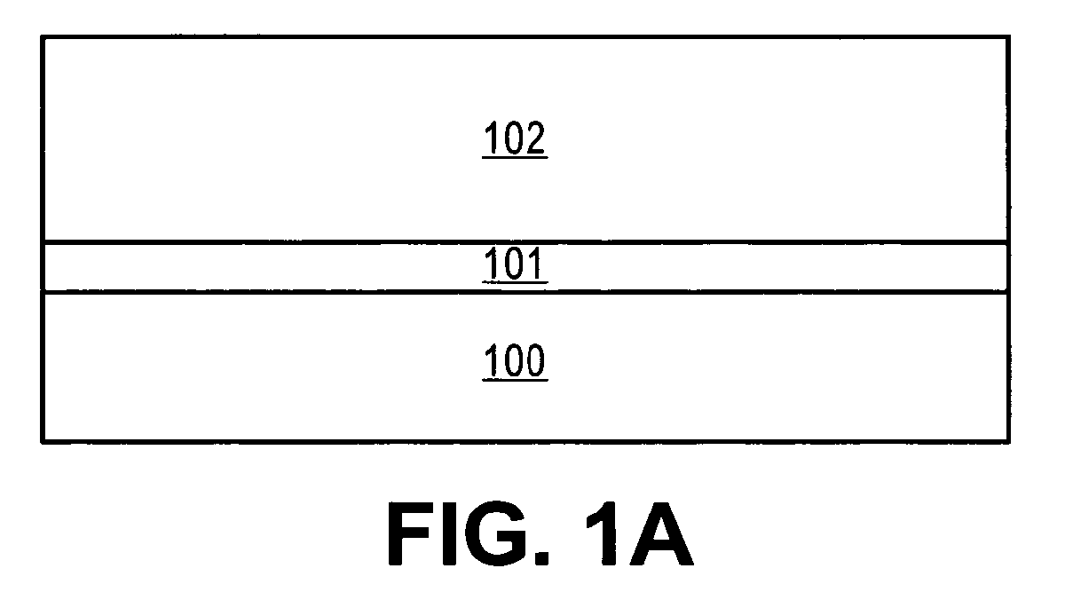
- FIGS. 1 a-1 d represent cross-sections of structures that may be formed when carrying out an embodiment of the method of the present invention. Features shown in these figures are not intended to be drawn to scale.
- a method for making a semiconductor device comprises forming a high-k gate dielectric layer on a substrate, and modifying a first portion of the high-k gate dielectric layer to ensure that it may be removed selectively to a second portion of the high-k gate dielectric layer.
- a high-k gate dielectric layer is formed on a substrate.
- the substrate may comprise a bulk silicon or silicon-on-insulator substructure.
- the substrate may comprise other materials -- which may or may not be combined with silicon -- such as: germanium, indium antimonide, lead telluride, indium arsenide, indium phosphide, gallium arsenide, or gallium antimonide.
- the high-k gate dielectric layer will comprise a material with a dielectric constant that is greater than the dielectric constant of silicon dioxide.
- the high-k gate dielectric layer has a dielectric constant that is at least about twice that of silicon dioxide, i.e., a dielectric constant that is greater than about 8.
- Materials for making the high-k gate dielectric layer include: hafnium oxide, hafnium silicon oxide, lanthanum oxide, zirconium oxide, zirconium silicon oxide, titanium oxide, tantalum oxide, barium strontium titanium oxide, barium titanium oxide, strontium titanium oxide, yttrium oxide, aluminum oxide, and lead scandium tantalum oxide. Particularly preferred are hafnium oxide, zirconium oxide, titanium oxide, and aluminum oxide.
- the high-k gate dielectric layer may be formed on the substrate using a conventional deposition method, e.g., a conventional chemical vapor deposition ("CVD"), low pressure CVD, or physical vapor deposition (“PVD”) process.
- a conventional atomic layer CVD process is used.
- a metal oxide precursor e.g., a metal chloride
- steam may be fed at selected flow rates into a CVD reactor, which is then operated at a selected temperature and pressure to generate an atomically smooth interface between the substrate and the high-k gate dielectric layer.
- the CVD reactor should be operated long enough to form a layer with the desired thickness.
- the high-k gate dielectric layer should be less than about 40 angstroms thick, and more preferably between about 5 angstroms and about 20 angstroms thick - i.e., less than or equal to about 5 monolayers thick.
- the high-k gate dielectric layer may include undesirable impurities, e.g., residual chlorine, which render that layer incompatible with polysilicon. That layer may be purified by depositing a sacrificial layer on its surface, then removing the sacrificial layer after it has absorbed a significant number of the impurities initially present in the high-k gate dielectric layer.
- the high-k gate dielectric layer may be purified by reducing it to a metal layer, then reoxidizing that metal layer. It may be desirable to increase the oxygen content of the high-k gate dielectric layer, e.g., via a wet or dry oxidation process.
- the high-k gate dielectric layer may be modified in other ways, e.g., by adding nitrogen to it, or intermediate layers may be placed between that film and the gate electrode.
- a gate electrode may be formed on that layer.
- the gate electrode comprises polysilicon.
- Such a gate electrode may be formed by initially depositing polysilicon layer 102 on dielectric layer 101 and substrate 100 - generating the figure 1a structure.
- Polysilicon layer 102 may be deposited using conventional methods and preferably is between about 500 angstroms and about 4,000 angstroms thick. Polysilicon layer 102 may then be etched to expose first portion 103 of high-k gate dielectric layer 101, generating the figure 1b structure.
- first portion 103 After etching polysilicon layer 102, exposed first portion 103 must be removed. Prior to etching first portion 103, however, the method of the present invention modifies first portion 103, as shown in figure 1c, to ensure that it may be removed selectively to second portion 104 of high-k gate dielectric layer 101.
- First portion 103 of high-k gate dielectric layer 101 may be modified by adding impurities to that portion of the dielectric layer.
- the impurities comprise a halogen, which may be embodied in a halogen molecule or be combined with hydrogen to form a halide.
- a plasma enhanced chemical vapor deposition (“PECVD”) process may be used to add impurities to first portion 103 of high-k gate dielectric layer 101.
- PECVD plasma enhanced chemical vapor deposition
- a halogen or halide gas (or a combination of such gases) may be fed into a reactor prior to striking a plasma.
- the reactor should be operated under the appropriate conditions (e.g., temperature, pressure, radio frequency, and power) for a sufficient time to modify first portion 103 of high-k gate dielectric layer 101 to ensure that it may be removed selectively to other materials.
- a low power PECVD process e.g., one taking place at less than about 200 watts, is used.
- hydrogen bromide (“HBr”) and chlorine (“Cl 2 ”) gases are fed into the reactor at appropriate flow rates to ensure that a plasma generated from those gases will modify first portion 103 of high-k gate dielectric layer 101 in the desired manner.
- wafer bias preferably about 100 watts
- Plasma exposure lasting less than about one minute, and perhaps as short as 5 seconds, may be adequate to cause that conversion.
- first portion 103 of high-k dielectric layer 101 Although a few examples of processes for modifying first portion 103 of high-k dielectric layer 101 are described here, other treatments may be used, as will be apparent to those skilled in the art. The process used to modify first portion 103 is thus not limited to those described above.
- the method of the present invention contemplates using any suitable wet or dry chemical treatment that adds impurities to first portion 103 of high-k dielectric layer 101 to ensure that first portion 103 may be removed selectively to second portion 104 of high-k gate dielectric layer 101.
- first portion 103 After first portion 103 has been modified, it is removed.
- the presence of the added impurities enables first portion 103 to be removed, i.e., etched, selectively to second portion 104 to generate the figure 1d structure.
- first portion 103 is removed by exposing it to a relatively strong acid, e.g., a halide based acid (such as hydrobromic or hydrochloric acid) or phosphoric acid.
- a relatively strong acid e.g., a halide based acid (such as hydrobromic or hydrochloric acid) or phosphoric acid.
- the acid When a halide based acid is used, the acid preferably contains between about 0.5% and about 10% HBr or HCl by volume - and more preferably about 5% by volume. An etch process that uses such an acid may take place at or near room temperature, and last for between about 5 and about 30 minutes - although a longer exposure may be used if desired. When phosphoric acid is used, the acid preferably contains between about 75% and about 95% H 3 PO 4 by volume. An etch process that uses such an acid preferably takes place at between about 140°C and about 180°C, and more preferably at about 160°C. When such an acid is used, the exposure step should last between about 30 seconds and about 5 minutes - and preferably for about one minute for a 20 angstrom thick film.
- first portion 103 selective to second portion 104 processes for removing first portion 103 selective to second portion 104 are described here, other processes may be used, as will be apparent to those skilled in the art.
- the process used to etch first portion 103 is thus not limited to those described above.
- the method of the present invention contemplates using any suitable treatment that removes first portion 103 of high-k dielectric layer 101 selectively to second portion 104 of high-k gate dielectric layer 101.
- the gate electrode preferably comprises polysilicon, it may alternatively be formed from various metals with which high-k gate dielectrics may be used. In addition, the gate electrode may comprise a combination of polysilicon and one or more metal or semi-metal materials.
- modifying first portion 103 of high-k gate dielectric layer 101 anisotropically, leaving adjacent structures unaffected by that process step, may ensure that a subsequent wet etch process will not appreciably etch into the underlying substrate or the adjoining second portion.
- this process when this process is used to etch the high-k dielectric layer, the underlying substrate should not sustain any meaningful damage and the gate electrode should not be lifted or undercut to a significant degree.
- the embodiments described above are examples of processes that may enable a first portion of a high-k gate dielectric layer to be removed selectively to a second portion of that layer, the present invention is not limited to these particular embodiments.
- the present invention contemplates other processes for transforming part of a high-k gate dielectric layer to enable its selective removal, ensuring that the dielectric layer etch will not significantly damage the underlying substrate or undercut the gate electrode.
Landscapes
- Insulated Gate Type Field-Effect Transistor (AREA)
- Electrodes Of Semiconductors (AREA)
Abstract
Description
- The present invention relates to methods for making semiconductor devices, in particular, semiconductor devices that include high-k gate dielectric layers.
- Conventional processes for etching high-k gate dielectric layers apply anisotropic plasma etch and isotropic wet etch techniques. Dry etch processes may damage the substrate that lies beneath the high-k gate dielectric, if they etch the substrate at a significantly faster rate than they etch the dielectric. Although wet etch processes may etch the dielectric selective to the underlying substrate, such processes may etch the dielectric where it is located beneath the gate electrode, which may weaken or lift that structure.
- Accordingly, there is a need for an improved process for making a semiconductor device that includes a high-k gate dielectric. There is a need for such a process that etches the exposed part of the high-k film selective to the underlying substrate and selective to the part of that film that the gate electrode covers. The method of the present invention provides such a process.
- Figures 1 a-1 d represent cross-sections of structures that may be formed when carrying out an embodiment of the method of the present invention. Features shown in these figures are not intended to be drawn to scale.
- A method for making a semiconductor device is described. That method comprises forming a high-k gate dielectric layer on a substrate, and modifying a first portion of the high-k gate dielectric layer to ensure that it may be removed selectively to a second portion of the high-k gate dielectric layer. In the following description, a number of details are set forth to provide a thorough explanation of the present invention. It will be apparent to those skilled in the art, however, that the invention may be practiced in many ways other than those expressly described here. The invention is thus not limited by the specific details disclosed below.
- In the method of the present invention, a high-k gate dielectric layer is formed on a substrate. The substrate may comprise a bulk silicon or silicon-on-insulator substructure. Alternatively, the substrate may comprise other materials -- which may or may not be combined with silicon -- such as: germanium, indium antimonide, lead telluride, indium arsenide, indium phosphide, gallium arsenide, or gallium antimonide. Although several examples of materials from which the substrate may be formed are described here, any material that may serve as a foundation upon which a semiconductor device may be built falls within the spirit and scope of the present invention.
- The high-k gate dielectric layer will comprise a material with a dielectric constant that is greater than the dielectric constant of silicon dioxide. Preferably, the high-k gate dielectric layer has a dielectric constant that is at least about twice that of silicon dioxide, i.e., a dielectric constant that is greater than about 8. Materials for making the high-k gate dielectric layer include: hafnium oxide, hafnium silicon oxide, lanthanum oxide, zirconium oxide, zirconium silicon oxide, titanium oxide, tantalum oxide, barium strontium titanium oxide, barium titanium oxide, strontium titanium oxide, yttrium oxide, aluminum oxide, and lead scandium tantalum oxide. Particularly preferred are hafnium oxide, zirconium oxide, titanium oxide, and aluminum oxide. Although a few examples of materials that may be used to form high-k gate dielectric layer are described here, that layer may be made from other materials, as will be apparent to those skilled in the art.
- The high-k gate dielectric layer may be formed on the substrate using a conventional deposition method, e.g., a conventional chemical vapor deposition ("CVD"), low pressure CVD, or physical vapor deposition ("PVD") process. Preferably, a conventional atomic layer CVD process is used. In such a process, a metal oxide precursor (e.g., a metal chloride) and steam may be fed at selected flow rates into a CVD reactor, which is then operated at a selected temperature and pressure to generate an atomically smooth interface between the substrate and the high-k gate dielectric layer. The CVD reactor should be operated long enough to form a layer with the desired thickness. In most applications, the high-k gate dielectric layer should be less than about 40 angstroms thick, and more preferably between about 5 angstroms and about 20 angstroms thick - i.e., less than or equal to about 5 monolayers thick.
- As deposited, the high-k gate dielectric layer may include undesirable impurities, e.g., residual chlorine, which render that layer incompatible with polysilicon. That layer may be purified by depositing a sacrificial layer on its surface, then removing the sacrificial layer after it has absorbed a significant number of the impurities initially present in the high-k gate dielectric layer. Alternatively, the high-k gate dielectric layer may be purified by reducing it to a metal layer, then reoxidizing that metal layer. It may be desirable to increase the oxygen content of the high-k gate dielectric layer, e.g., via a wet or dry oxidation process. To ensure compatibility with a polysilicon based gate electrode, the high-k gate dielectric layer may be modified in other ways, e.g., by adding nitrogen to it, or intermediate layers may be placed between that film and the gate electrode.
- After the high-k gate dielectric layer is formed on the substrate, a gate electrode may be formed on that layer. In a preferred embodiment, the gate electrode comprises polysilicon. Such a gate electrode may be formed by initially depositing
polysilicon layer 102 ondielectric layer 101 and substrate 100 - generating the figure 1a structure.Polysilicon layer 102 may be deposited using conventional methods and preferably is between about 500 angstroms and about 4,000 angstroms thick.Polysilicon layer 102 may then be etched to exposefirst portion 103 of high-kgate dielectric layer 101, generating the figure 1b structure. - After etching
polysilicon layer 102, exposedfirst portion 103 must be removed. Prior to etchingfirst portion 103, however, the method of the present invention modifiesfirst portion 103, as shown in figure 1c, to ensure that it may be removed selectively tosecond portion 104 of high-kgate dielectric layer 101.First portion 103 of high-kgate dielectric layer 101 may be modified by adding impurities to that portion of the dielectric layer. In a preferred embodiment, the impurities comprise a halogen, which may be embodied in a halogen molecule or be combined with hydrogen to form a halide. - A plasma enhanced chemical vapor deposition ("PECVD") process may be used to add impurities to
first portion 103 of high-kgate dielectric layer 101. In such a PECVD process, a halogen or halide gas (or a combination of such gases) may be fed into a reactor prior to striking a plasma. The reactor should be operated under the appropriate conditions (e.g., temperature, pressure, radio frequency, and power) for a sufficient time to modifyfirst portion 103 of high-kgate dielectric layer 101 to ensure that it may be removed selectively to other materials. In a preferred embodiment, a low power PECVD process, e.g., one taking place at less than about 200 watts, is used. - In a particularly preferred embodiment, hydrogen bromide ("HBr") and chlorine ("Cl2") gases are fed into the reactor at appropriate flow rates to ensure that a plasma generated from those gases will modify
first portion 103 of high-kgate dielectric layer 101 in the desired manner. Between about 50 and about 100 watts wafer bias (preferably about 100 watts) may be applied for a sufficient time to complete the desired transformation offirst portion 103. Plasma exposure lasting less than about one minute, and perhaps as short as 5 seconds, may be adequate to cause that conversion. - Although a few examples of processes for modifying
first portion 103 of high-k dielectric layer 101 are described here, other treatments may be used, as will be apparent to those skilled in the art. The process used to modifyfirst portion 103 is thus not limited to those described above. The method of the present invention contemplates using any suitable wet or dry chemical treatment that adds impurities tofirst portion 103 of high-k dielectric layer 101 to ensure thatfirst portion 103 may be removed selectively tosecond portion 104 of high-kgate dielectric layer 101. - After
first portion 103 has been modified, it is removed. The presence of the added impurities enablesfirst portion 103 to be removed, i.e., etched, selectively tosecond portion 104 to generate the figure 1d structure. In a preferred embodiment,first portion 103 is removed by exposing it to a relatively strong acid, e.g., a halide based acid (such as hydrobromic or hydrochloric acid) or phosphoric acid. - When a halide based acid is used, the acid preferably contains between about 0.5% and about 10% HBr or HCl by volume - and more preferably about 5% by volume. An etch process that uses such an acid may take place at or near room temperature, and last for between about 5 and about 30 minutes - although a longer exposure may be used if desired. When phosphoric acid is used, the acid preferably contains between about 75% and about 95% H3PO4 by volume. An etch process that uses such an acid preferably takes place at between about 140°C and about 180°C, and more preferably at about 160°C. When such an acid is used, the exposure step should last between about 30 seconds and about 5 minutes - and preferably for about one minute for a 20 angstrom thick film.
- Although a few examples of processes for removing
first portion 103 selective tosecond portion 104 are described here, other processes may be used, as will be apparent to those skilled in the art. The process used to etchfirst portion 103 is thus not limited to those described above. The method of the present invention contemplates using any suitable treatment that removesfirst portion 103 of high-k dielectric layer 101 selectively tosecond portion 104 of high-kgate dielectric layer 101. - Because additional steps that are generally used to complete the semiconductor device are well known to those skilled in the art, they will not be described in more detail here. Although the gate electrode preferably comprises polysilicon, it may alternatively be formed from various metals with which high-k gate dielectrics may be used. In addition, the gate electrode may comprise a combination of polysilicon and one or more metal or semi-metal materials.
- As described above, modifying
first portion 103 of high-kgate dielectric layer 101 anisotropically, leaving adjacent structures unaffected by that process step, may ensure that a subsequent wet etch process will not appreciably etch into the underlying substrate or the adjoining second portion. As a consequence, when this process is used to etch the high-k dielectric layer, the underlying substrate should not sustain any meaningful damage and the gate electrode should not be lifted or undercut to a significant degree. - Although the embodiments described above are examples of processes that may enable a first portion of a high-k gate dielectric layer to be removed selectively to a second portion of that layer, the present invention is not limited to these particular embodiments. The present invention contemplates other processes for transforming part of a high-k gate dielectric layer to enable its selective removal, ensuring that the dielectric layer etch will not significantly damage the underlying substrate or undercut the gate electrode.
- Although the foregoing description has specified certain steps and materials that may be used in the method of the present invention, those skilled in the art will appreciate that many modifications and substitutions may be made. Accordingly, it is intended that all such modifications, alterations, substitutions and additions be considered to fall within the spirit and scope of the invention as defined by the appended claims.
Claims (15)
- A method for making a semiconductor device comprising:forming a high-k gate dielectric layer on a substrate; andmodifying a first portion of the high-k gate dielectric layer to ensure that it may be removed selectively to a second portion of the high-k gate dielectric layer.
- The method of claim 1 wherein the high-k gate dielectric layer is formed by atomic layer chemical vapor deposition, is between about 5 angstroms and about 40 angstroms thick, and comprises a material selected from the group consisting of hafnium oxide, hafnium silicon oxide, lanthanum oxide, zirconium oxide, zirconium silicon oxide, titanium oxide, tantalum oxide, barium strontium titanium oxide, barium titanium oxide, strontium titanium oxide, yttrium oxide, aluminum oxide, and lead scandium tantalum oxide.
- The method of claim 1 or 2 further comprising removing the first portion of the high-k gate dielectric layer selective to the second portion of the high-k gate dielectric layer.
- The method of one of the preceding claims wherein the first portion of the high-k gate dielectric layer is modified by adding impurities to the first portion of the high-k gate dielectric layer.
- The method of claim 4 wherein the impurities comprise a halogen.
- The method of claim 4 wherein the impurities comprise a halide.
- The method of one of the claims 4 to 6 wherein a plasma enhanced chemical vapor deposition process is used to add the impurities.
- The method of one of the claims 3 to 7 wherein the first portion of the high-k gate dielectric layer is removed selectively to the second portion of the high-k gate dielectric layer by exposing the first portion of the high-k gate dielectric layer to an acid.
- The method of claim 8 wherein the acid comprises a halide based acid.
- The method of claim 8 wherein the acid comprises phosphoric acid.
- The method of one of the preceding claims including:forming a gate electrode on the high-k gate dielectric layer;etching the gate electrode to expose the first portion of the high-k gate dielectric layer;adding impurities to the first portion of the high-k gate dielectric layer; andremoving the first portion of the high-k gate dielectric layer selective to the second portion of the high-k gate dielectric layer.
- The method of claim 11 wherein the gate electrode comprises polysilicon.
- The method of claim 11 wherein the gate electrode is a metal gate electrode.
- The method of one of the claims 11 to 13 wherein a low power plasma enhanced chemical vapor deposition process is used to add impurities that comprise a mixture of a halogen and a halide.
- The method of one of the claims 11 to 14 wherein the first portion of the high-k gate dielectric layer is removed selectively to the second portion of the high-k gate dielectric layer by exposing the first portion of the high-k gate dielectric layer to an acid that is selected from the group consisting of a halide based acid and phosphoric acid.
Applications Claiming Priority (2)
| Application Number | Priority Date | Filing Date | Title |
|---|---|---|---|
| US10/652,546 US7037845B2 (en) | 2003-08-28 | 2003-08-28 | Selective etch process for making a semiconductor device having a high-k gate dielectric |
| US652546 | 2003-08-28 |
Publications (1)
| Publication Number | Publication Date |
|---|---|
| EP1511073A1 true EP1511073A1 (en) | 2005-03-02 |
Family
ID=34104750
Family Applications (1)
| Application Number | Title | Priority Date | Filing Date |
|---|---|---|---|
| EP04017225A Ceased EP1511073A1 (en) | 2003-08-28 | 2004-07-21 | A selective etch process for making a semiconductor device having a high-k gate dielectric |
Country Status (6)
| Country | Link |
|---|---|
| US (1) | US7037845B2 (en) |
| EP (1) | EP1511073A1 (en) |
| KR (1) | KR100716689B1 (en) |
| CN (1) | CN1591786B (en) |
| TW (1) | TWI239563B (en) |
| WO (1) | WO2005024929A1 (en) |
Cited By (1)
| Publication number | Priority date | Publication date | Assignee | Title |
|---|---|---|---|---|
| US7037845B2 (en) | 2003-08-28 | 2006-05-02 | Intel Corporation | Selective etch process for making a semiconductor device having a high-k gate dielectric |
Families Citing this family (21)
| Publication number | Priority date | Publication date | Assignee | Title |
|---|---|---|---|---|
| US7037863B2 (en) * | 2002-09-10 | 2006-05-02 | Samsung Electronics Co., Ltd. | Post thermal treatment methods of forming high dielectric layers over interfacial layers in integrated circuit devices |
| US7413996B2 (en) * | 2003-04-14 | 2008-08-19 | Lsi Corporation | High k gate insulator removal |
| US20050064716A1 (en) * | 2003-04-14 | 2005-03-24 | Hong Lin | Plasma removal of high k metal oxide |
| JP2005038897A (en) * | 2003-07-15 | 2005-02-10 | Dainippon Screen Mfg Co Ltd | Substrate processing method and apparatus |
| JPWO2005013374A1 (en) * | 2003-08-05 | 2006-09-28 | 富士通株式会社 | Semiconductor device and manufacturing method of semiconductor device |
| US7153734B2 (en) | 2003-12-29 | 2006-12-26 | Intel Corporation | CMOS device with metal and silicide gate electrodes and a method for making it |
| US7144783B2 (en) * | 2004-04-30 | 2006-12-05 | Intel Corporation | Reducing gate dielectric material to form a metal gate electrode extension |
| US7564108B2 (en) * | 2004-12-20 | 2009-07-21 | Taiwan Semiconductor Manufacturing Company, Ltd. | Nitrogen treatment to improve high-k gate dielectrics |
| US20080001237A1 (en) * | 2006-06-29 | 2008-01-03 | Taiwan Semiconductor Manufacturing Company, Ltd. | Semiconductor device having nitrided high-k gate dielectric and metal gate electrode and methods of forming same |
| US20080315310A1 (en) * | 2007-06-19 | 2008-12-25 | Willy Rachmady | High k dielectric materials integrated into multi-gate transistor structures |
| US7645663B2 (en) | 2007-07-18 | 2010-01-12 | Infineon Technologies Ag | Method of producing non volatile memory device |
| US8247861B2 (en) | 2007-07-18 | 2012-08-21 | Infineon Technologies Ag | Semiconductor device and method of making same |
| US7998820B2 (en) | 2007-08-07 | 2011-08-16 | Taiwan Semiconductor Manufacturing Company, Ltd. | High-k gate dielectric and method of manufacture |
| US8030163B2 (en) * | 2007-12-26 | 2011-10-04 | Intel Corporation | Reducing external resistance of a multi-gate device using spacer processing techniques |
| US7763943B2 (en) * | 2007-12-26 | 2010-07-27 | Intel Corporation | Reducing external resistance of a multi-gate device by incorporation of a partial metallic fin |
| US20090206404A1 (en) * | 2008-02-15 | 2009-08-20 | Ravi Pillarisetty | Reducing external resistance of a multi-gate device by silicidation |
| US8264048B2 (en) * | 2008-02-15 | 2012-09-11 | Intel Corporation | Multi-gate device having a T-shaped gate structure |
| US8101495B2 (en) | 2008-03-13 | 2012-01-24 | Infineon Technologies Ag | MIM capacitors in semiconductor components |
| KR101634748B1 (en) | 2009-12-08 | 2016-07-11 | 삼성전자주식회사 | method for manufacturing MOS transistor and forming method of integrated circuit using the sime |
| US9570573B1 (en) | 2015-08-10 | 2017-02-14 | Globalfoundries Inc. | Self-aligned gate tie-down contacts with selective etch stop liner |
| US9905671B2 (en) | 2015-08-19 | 2018-02-27 | International Business Machines Corporation | Forming a gate contact in the active area |
Citations (9)
| Publication number | Priority date | Publication date | Assignee | Title |
|---|---|---|---|---|
| JPH05175174A (en) * | 1991-12-20 | 1993-07-13 | Nec Corp | Reactive dry etching method for dielectric film |
| US5368687A (en) * | 1993-03-15 | 1994-11-29 | Micron Technology, Inc. | Semiconductor processing method of etching insulating inorganic metal oxide materials and method of cleaning metals from the surface of semiconductor wafers |
| JP2000216142A (en) * | 1999-01-22 | 2000-08-04 | Tokyo Electron Ltd | Etching method |
| US6432779B1 (en) * | 2000-05-18 | 2002-08-13 | Motorola, Inc. | Selective removal of a metal oxide dielectric |
| US20030104706A1 (en) * | 2001-12-04 | 2003-06-05 | Matsushita Electric Industrial Co., Ltd. | Wet-etching method and method for manufacturing semiconductor device |
| WO2004021409A2 (en) * | 2002-08-27 | 2004-03-11 | Tokyo Electron Limited | A method and system to enhance the removal of high-k-dielectric materials |
| WO2004030049A2 (en) * | 2002-09-27 | 2004-04-08 | Tokyo Electron Limited | A method and system for etching high-k dielectric materials |
| US6764898B1 (en) * | 2002-05-16 | 2004-07-20 | Advanced Micro Devices, Inc. | Implantation into high-K dielectric material after gate etch to facilitate removal |
| US20040203246A1 (en) * | 2003-04-14 | 2004-10-14 | Arvind Kamath | High k gate insulator removal |
Family Cites Families (28)
| Publication number | Priority date | Publication date | Assignee | Title |
|---|---|---|---|---|
| NL188432C (en) * | 1980-12-26 | 1992-06-16 | Nippon Telegraph & Telephone | METHOD FOR MANUFACTURING A MOSFET |
| AU5669794A (en) * | 1992-12-11 | 1994-07-04 | Intel Corporation | A mos transistor having a composite gate electrode and method of fabrication |
| US5516399A (en) * | 1994-06-30 | 1996-05-14 | International Business Machines Corporation | Contactless real-time in-situ monitoring of a chemical etching |
| US5753560A (en) * | 1996-10-31 | 1998-05-19 | Motorola, Inc. | Method for fabricating a semiconductor device using lateral gettering |
| US5891798A (en) * | 1996-12-20 | 1999-04-06 | Intel Corporation | Method for forming a High dielectric constant insulator in the fabrication of an integrated circuit |
| US6063698A (en) * | 1997-06-30 | 2000-05-16 | Motorola, Inc. | Method for manufacturing a high dielectric constant gate oxide for use in semiconductor integrated circuits |
| US6087261A (en) * | 1997-09-30 | 2000-07-11 | Fujitsu Limited | Method for production of semiconductor device |
| US20020197790A1 (en) * | 1997-12-22 | 2002-12-26 | Kizilyalli Isik C. | Method of making a compound, high-K, gate and capacitor insulator layer |
| US6121094A (en) * | 1998-07-21 | 2000-09-19 | Advanced Micro Devices, Inc. | Method of making a semiconductor device with a multi-level gate structure |
| US6320244B1 (en) * | 1999-01-12 | 2001-11-20 | Agere Systems Guardian Corp. | Integrated circuit device having dual damascene capacitor |
| FR2797999B1 (en) * | 1999-08-31 | 2003-08-08 | St Microelectronics Sa | METHOD FOR MANUFACTURING AN INTEGRATED CAPACITY ON A SILICON SUBSTRATE |
| US6184072B1 (en) * | 2000-05-17 | 2001-02-06 | Motorola, Inc. | Process for forming a high-K gate dielectric |
| US6475974B1 (en) * | 2000-09-01 | 2002-11-05 | Dow Corning Corporation | Mechanical microemulsions of blended silicones |
| US6660660B2 (en) * | 2000-10-10 | 2003-12-09 | Asm International, Nv. | Methods for making a dielectric stack in an integrated circuit |
| JP2002134739A (en) * | 2000-10-19 | 2002-05-10 | Mitsubishi Electric Corp | Semiconductor device and manufacturing method thereof |
| US6475874B2 (en) * | 2000-12-07 | 2002-11-05 | Advanced Micro Devices, Inc. | Damascene NiSi metal gate high-k transistor |
| US6544906B2 (en) * | 2000-12-21 | 2003-04-08 | Texas Instruments Incorporated | Annealing of high-k dielectric materials |
| US6514828B2 (en) * | 2001-04-20 | 2003-02-04 | Micron Technology, Inc. | Method of fabricating a highly reliable gate oxide |
| US6420279B1 (en) * | 2001-06-28 | 2002-07-16 | Sharp Laboratories Of America, Inc. | Methods of using atomic layer deposition to deposit a high dielectric constant material on a substrate |
| US6677254B2 (en) * | 2001-07-23 | 2004-01-13 | Applied Materials, Inc. | Processes for making a barrier between a dielectric and a conductor and products produced therefrom |
| US6573193B2 (en) | 2001-08-13 | 2003-06-03 | Taiwan Semiconductor Manufacturing Co., Ltd | Ozone-enhanced oxidation for high-k dielectric semiconductor devices |
| US6797599B2 (en) * | 2001-08-31 | 2004-09-28 | Texas Instruments Incorporated | Gate structure and method |
| US6455330B1 (en) * | 2002-01-28 | 2002-09-24 | Taiwan Semiconductor Manufacturing Company | Methods to create high-k dielectric gate electrodes with backside cleaning |
| US6617209B1 (en) * | 2002-02-22 | 2003-09-09 | Intel Corporation | Method for making a semiconductor device having a high-k gate dielectric |
| US6617210B1 (en) * | 2002-05-31 | 2003-09-09 | Intel Corporation | Method for making a semiconductor device having a high-k gate dielectric |
| US6696327B1 (en) * | 2003-03-18 | 2004-02-24 | Intel Corporation | Method for making a semiconductor device having a high-k gate dielectric |
| US6855639B1 (en) * | 2003-08-01 | 2005-02-15 | Intel Corporation | Precise patterning of high-K films |
| US7037845B2 (en) | 2003-08-28 | 2006-05-02 | Intel Corporation | Selective etch process for making a semiconductor device having a high-k gate dielectric |
-
2003
- 2003-08-28 US US10/652,546 patent/US7037845B2/en not_active Expired - Fee Related
-
2004
- 2004-07-21 EP EP04017225A patent/EP1511073A1/en not_active Ceased
- 2004-08-25 WO PCT/US2004/027747 patent/WO2005024929A1/en not_active Ceased
- 2004-08-26 TW TW093125596A patent/TWI239563B/en active
- 2004-08-27 KR KR1020040068106A patent/KR100716689B1/en not_active Expired - Fee Related
- 2004-08-30 CN CN2004100570938A patent/CN1591786B/en not_active Expired - Fee Related
Patent Citations (9)
| Publication number | Priority date | Publication date | Assignee | Title |
|---|---|---|---|---|
| JPH05175174A (en) * | 1991-12-20 | 1993-07-13 | Nec Corp | Reactive dry etching method for dielectric film |
| US5368687A (en) * | 1993-03-15 | 1994-11-29 | Micron Technology, Inc. | Semiconductor processing method of etching insulating inorganic metal oxide materials and method of cleaning metals from the surface of semiconductor wafers |
| JP2000216142A (en) * | 1999-01-22 | 2000-08-04 | Tokyo Electron Ltd | Etching method |
| US6432779B1 (en) * | 2000-05-18 | 2002-08-13 | Motorola, Inc. | Selective removal of a metal oxide dielectric |
| US20030104706A1 (en) * | 2001-12-04 | 2003-06-05 | Matsushita Electric Industrial Co., Ltd. | Wet-etching method and method for manufacturing semiconductor device |
| US6764898B1 (en) * | 2002-05-16 | 2004-07-20 | Advanced Micro Devices, Inc. | Implantation into high-K dielectric material after gate etch to facilitate removal |
| WO2004021409A2 (en) * | 2002-08-27 | 2004-03-11 | Tokyo Electron Limited | A method and system to enhance the removal of high-k-dielectric materials |
| WO2004030049A2 (en) * | 2002-09-27 | 2004-04-08 | Tokyo Electron Limited | A method and system for etching high-k dielectric materials |
| US20040203246A1 (en) * | 2003-04-14 | 2004-10-14 | Arvind Kamath | High k gate insulator removal |
Non-Patent Citations (5)
| Title |
|---|
| "PROCESS FOR SELECTIVE ETCHING OF TANTALIUM OXIDE", IBM TECHNICAL DISCLOSURE BULLETIN, IBM CORP. NEW YORK, US, vol. 27, no. 12, May 1985 (1985-05-01), pages 7238, XP000807046, ISSN: 0018-8689 * |
| BERNETT J ET AL: "Wet Etch Enhancement of HfO2 Films by Implant Processing", DIFFUSION AND DEFECT DATA. SOLID STATE DATA. PART B, SOLID STATE PHENOMENA, VADUZ, LI, vol. 92, 2003, pages 11 - 14, XP008029227, ISSN: 1012-0394 * |
| CHRISTENSON K ET AL: "SELECTIVE WET ETCHING OF HIGH-K GATE DIELECTRICS", DIFFUSION AND DEFECT DATA. SOLID STATE DATA. PART B, SOLID STATE PHENOMENA, VADUZ, LI, vol. 92, 2003, pages 129 - 132, XP008023469, ISSN: 1012-0394 * |
| PATENT ABSTRACTS OF JAPAN vol. 017, no. 579 (E - 1451) 21 October 1993 (1993-10-21) * |
| PATENT ABSTRACTS OF JAPAN vol. 2000, no. 11 3 January 2001 (2001-01-03) * |
Cited By (2)
| Publication number | Priority date | Publication date | Assignee | Title |
|---|---|---|---|---|
| US7037845B2 (en) | 2003-08-28 | 2006-05-02 | Intel Corporation | Selective etch process for making a semiconductor device having a high-k gate dielectric |
| KR100716689B1 (en) | 2003-08-28 | 2007-05-09 | 인텔 코오퍼레이션 | A selective etch process for making a semiconductor device having a high-k gate dielectric |
Also Published As
| Publication number | Publication date |
|---|---|
| CN1591786A (en) | 2005-03-09 |
| KR20050021943A (en) | 2005-03-07 |
| US20050048791A1 (en) | 2005-03-03 |
| KR100716689B1 (en) | 2007-05-09 |
| TWI239563B (en) | 2005-09-11 |
| WO2005024929A1 (en) | 2005-03-17 |
| TW200509244A (en) | 2005-03-01 |
| CN1591786B (en) | 2010-06-16 |
| US7037845B2 (en) | 2006-05-02 |
Similar Documents
| Publication | Publication Date | Title |
|---|---|---|
| US7037845B2 (en) | Selective etch process for making a semiconductor device having a high-k gate dielectric | |
| US6939815B2 (en) | Method for making a semiconductor device having a high-k gate dielectric | |
| US6713358B1 (en) | Method for making a semiconductor device having a high-k gate dielectric | |
| US6689675B1 (en) | Method for making a semiconductor device having a high-k gate dielectric | |
| US6787440B2 (en) | Method for making a semiconductor device having an ultra-thin high-k gate dielectric | |
| US6709911B1 (en) | Method for making a semiconductor device having a high-k gate dielectric | |
| US6897134B2 (en) | Method for making a semiconductor device having a high-k gate dielectric | |
| JP5154222B2 (en) | Planarization of semiconductor structures for replacement metal gate formation. | |
| US7442983B2 (en) | Method for making a semiconductor device having a high-k gate dielectric | |
| US7176090B2 (en) | Method for making a semiconductor device that includes a metal gate electrode | |
| CN100440439C (en) | Method for manufacturing semiconductor device having metal gate electrode | |
| US7384880B2 (en) | Method for making a semiconductor device having a high-k gate dielectric | |
| US6867102B2 (en) | Method for making a semiconductor device having a high-k gate dielectric | |
| US20040180523A1 (en) | Method for making a semiconductor device having a high-k gate dielectric | |
| US6893927B1 (en) | Method for making a semiconductor device with a metal gate electrode | |
| TWI253691B (en) | Plasma treatment and etching process for ultra-thin dielectric films | |
| US7575991B2 (en) | Removing a high-k gate dielectric | |
| US20050287746A1 (en) | Facilitating removal of sacrificial layers to form replacement metal gates | |
| JP2012038816A (en) | Manufacturing method of semiconductor device |
Legal Events
| Date | Code | Title | Description |
|---|---|---|---|
| PUAI | Public reference made under article 153(3) epc to a published international application that has entered the european phase |
Free format text: ORIGINAL CODE: 0009012 |
|
| 17P | Request for examination filed |
Effective date: 20040721 |
|
| AK | Designated contracting states |
Kind code of ref document: A1 Designated state(s): AT BE BG CH CY CZ DE DK EE ES FI FR GB GR HU IE IT LI LU MC NL PL PT RO SE SI SK TR |
|
| AX | Request for extension of the european patent |
Extension state: AL HR LT LV MK |
|
| AKX | Designation fees paid |
Designated state(s): AT BE BG CH CY CZ DE DK EE ES FI FR GB GR HU IE IT LI LU MC NL PL PT RO SE SI SK TR |
|
| 17Q | First examination report despatched |
Effective date: 20061129 |
|
| STAA | Information on the status of an ep patent application or granted ep patent |
Free format text: STATUS: THE APPLICATION HAS BEEN REFUSED |
|
| 18R | Application refused |
Effective date: 20091002 |