BACKGROUND OF THE INVENTION
1. Field of the Invention
The present invention relates to a magnetoresistive element and a
magnetic memory cell each including a magneto-sensitive layer of which
magnetization direction changes according to an external magnetic field
and a method of manufacturing the same. The invention also relates to a
magnetic memory device for recording/reading information by using a
change in the magnetization direction of a magneto-sensitive layer in the
magnetoresistive element and the magnetic memory cell and to a method
of manufacturing the same.
2. Description of the Related Art
Conventionally, as general memories used for an information
processor such as a computer or a communication device, volatile memories
such as a DRAM (Dynamic Random Access Memory) and an SRAM (Static
RAM) are used. The volatile memories have to be refreshed by always
supplying current to hold stored information. When the power source is
turned off, all of information is lost, so that a nonvolatile memory as means
for recording information has to be provided in addition to the volatile
memory. For example, a flash EEPROM, a magnetic hard disk drive, or
the like is used.
In the nonvolatile memories, as the speed of information
processing increases, increase in speed of an access is becoming an
important subject. Further, as a portable information device is being
rapidly spread and the performance is becoming higher, information device
development aiming at so-called ubiquitous computing which means that
information processing can be performed everywhere at any time is rapidly
being progressed. Development of a nonvolatile memory adapted for
higher-speed processing as a key device of such information device
development is in strong demand.
As a technique effective to increase the speed of the nonvolatile
memory, a magnetic random access memory (hereinbelow, described as
MRAM) is known in which magnetic memory elements each for storing
information in accordance with the magnetization direction along the axis
of easy magnetization of a ferromagnetic layer are arranged in a matrix.
The MRAM stores information by using a combination of the
magnetization directions in two ferromagnetic members. On the other
hand, stored information is read by detecting a resistance change (that is, a
change in current or voltage) which occurs between the case where the
magnetization direction is parallel with a reference direction and the case
where the magnetization direction is not parallel with the reference
direction. Since the MRAM operates with the principle, it is important
that the resistance change ratio is as high as possible to perform stable
writing and reading in the MRAM.
The MRAM currently used in practical utilizes the giant
magneto-resistive (GMR) effect. The GMR effect is a phenomenon such
that when two magnetic layers are disposed so that their axes of easy
magnetization are parallel with each other, in the case where the
magnetization directions of the layers are in parallel along the axis of easy
magnetization, the resistance value becomes the minimum. In the case
where the magnetization directions are not parallel with each other, the
resistance value becomes the maximum. An MRAM using a GMR element
capable of obtaining such a GMR effect (hereinbelow, described as
GMR-MRAM) is disclosed in, for example, U.S. Patent No. 5,343,422.
Recently, aiming at further improvement in storing speed, access
speed, and the like, an MRAM which has a TMR element using tunneling
magneto-resistive effect (TMR) in place of the GMR-MRAM is proposed
(hereinbelow, described as TMR-MRAM). The TMR effect is an effect such
that the tunnel current passing through an insulating layer changes in
accordance with relative angles of the magnetization directions in two
ferromagnetic layers sandwiching a very-thin insulating layer (tunnel
barrier layer). When the magnetization directions in the two
ferromagnetic layers are parallel with each other, the resistance value
becomes the minimum. On the contrary, when the magnetization
directions are not parallel with each other, the resistance value becomes
the maximum. In the TMR-MRAM, when the TMR element has a
configuration of, for example, "CoFe/aluminum oxide/CoFe", the resistance
change ratio is as high as 40% and the resistance value is also large.
Consequently, the TMR-MRAM can be easily matched with a
semiconductor device such as an MOSFET. Therefore, the TMR-MRAM
can easily obtain a higher output as compared with the GMR-MRAM, and
improvement in storage capacity and access speed is expected. In the
TMR-MRAM, a current magnetic field is generated by passing current to a
conductor as a write line disposed near the TMR element. By using the
current magnetic field, and the magnetization direction in the magnetic
layer of the TMR element is changed to a predetermined direction, thereby
storing information. As a method of reading stored information, a method
of passing current in the direction perpendicular to a tunnel barrier layer
and detecting a resistance change in the TMR element is known. Such
TMR-MRAM techniques are disclosed in U.S. Patent No. 5,629,922 and
Japanese Patent Laid-open No. Hei 9-91949. Recently, higher packing
density of a magnetic memory device is in increasing demand and,
accordingly, reduction in the size of the TMR element is also required. As
the TMR element is becoming finer, due to the influence of a
demagnetizing field generated by magnetic poles at both ends of the TMR
element, the magnetization direction in a magnetic layer (free
magnetization direction layer) for storing information becomes unstable
and it becomes difficult to hold recorded information. To solve the
problem, a structure in which a closed magnetic circuit is formed in
addition to the free magnetization direction layer around a conductor
(write line) near the TMR element is proposed (refer to, for example,
Japanese Patent Laid-open No. 2001-273759). According to Japanese
Patent Laid-open No. 2001-273759, since the free magnetization direction
layer related to recording is a component of the closed magnetic circuit, the
adverse influence by the demagnetizing field can be avoided and a
magnetic memory device of high packing density can be realized. Further,
in this case, both of two write lines extend in the closed magnetic circuit, so
that magnetization can be efficiently inverted.
Japanese Patent Laid-open No. 2001-273759, however, does not
disclose a concrete method of manufacturing the TMR-MRAM having the
structure in which the closed magnetic circuit is formed. In particular, a
closed magnetic circuit layer which forms the closed magnetic circuit in
cooperation with the free magnetization direction layer of the TMR element
has to have high dimensional precision and sufficient thickness in the
direction orthogonal to the substrate face in order to achieve smaller size
and higher packing density. It is expected that high mass productivity is
also important for future wide spread use in future. In such
circumstances, establishment of a manufacturing method capable of
realizing high dimensional precision and sufficient thickness is urgently
necessary.
SUMMARY OF THE INVENTION
The present invention has been achieved in consideration of such
problems and its first object is to provide a magneto-resistive element, a
magnetic memory cell, and a magnetic memory device including the
magneto-resistive element and the magnetic memory cell, each having a
compact configuration, to which information can be stably written by
efficiently using a magnetic field generated by current flowing in a
conductor, and which is formed with high precision. A second object is to
provide a method of manufacturing the magneto-resistive element, a
magnetic memory cell, and a magnetic memory device.
A magneto-resistive element according to the invention comprises:
a magnetic yoke disposed in correspondence with a partial region along an
extension direction of a conductor and constructed so as to surround
partially or entirely the periphery of the conductor; and a stacked body
including a magneto-sensitive layer of which magnetization direction
changes according to an external magnetic field, magnetically coupled to
the magnetic yoke, and constructed so that current flows in a direction
perpendicular to a stacked face. At least a part of the magnetic yoke is
constructed by a plating film.
A method of manufacturing a magneto-resistive element according
to the invention comprises: a step of forming a magnetic yoke so as to be
disposed in correspondence with a partial region along an extension
direction of a conductor and so as to surround partially or entirely the
periphery of the conductor; and a step of forming a stacked body including
a magneto-sensitive layer of which magnetization direction changes
according to an external magnetic field, magnetically coupled to the
magnetic yoke, and constructed so that current flows in a direction
perpendicular to a stacked face. In the step of forming the magnetic yoke,
at least a part of the magnetic yoke is formed by plating.
A magnetic memory cell according to the invention comprises a
pair of magneto-resistive elements each including: a magnetic yoke
disposed in correspondence with a partial region along an extension
direction of a conductor and constructed so as to surround partially or
entirely the periphery of the conductor; and a stacked body including a
magneto-sensitive layer of which magnetization direction changes
according to an external magnetic field, magnetically coupled to the
magnetic yoke, and constructed so that current flows in a direction
perpendicular to a stacked face. The pair of magneto-resistive elements
share a part of the magnetic yoke, and at least a part of the magnetic yoke
is constructed by a plating film.
A method of manufacturing a magnetic memory cell according to
the invention, the magnetic memory cell comprising a pair of
magneto-resistive elements each including a magnetic yoke and a stacked
body, comprises: a step of forming a pair of the magnetic yokes disposed in
correspondence with a partial region along an extension direction of a
conductor, constructed so as to surround partially or entirely the periphery
of the conductor, and partially sharing each other; and a step of forming a
pair of the stacked bodies each including a magneto-sensitive layer of
which magnetization direction changes according to an external magnetic
field, magnetically coupled to the pair of magnetic yokes, and constructed
so that current flows in a direction perpendicular to a stacked face. In the
step of forming the pair of magnetic yokes, at least a part of the pair of
magnetic yokes is formed by plating.
A magnetic memory device according to a first aspect of the
invention comprises: a first write line; a second write line extending so as
to cross the first write line; and a magneto-resistive element. The
magneto-resistive element includes: a magnetic yoke disposed in
correspondence with a region in which the first and second write lines cross
each other and constructed so as to surround partially or entirely the
periphery of the first and second write lines; and a stacked body including
a magneto-sensitive layer of which magnetization direction changes
according to an external magnetic field, magnetically coupled to the
magnetic yoke, and constructed so that current flows in a direction
perpendicular to a stacked face. At least a part of the magnetic yoke is
constructed by a plating film.
A magnetic memory device according to a second aspect of the
invention comprises: a first write line; a second write line extending so as
to cross the first write line; and a pair of magneto-resistive elements.
Each of the pair of magneto-resistive elements includes: a magnetic yoke
disposed in correspondence with a region in which the first and second
write lines cross each other and constructed so as to surround partially or
entirely the periphery of the first and second write lines; and a stacked
body including a magneto-sensitive layer of which magnetization direction
changes according to an external magnetic field, magnetically coupled to
the magnetic yoke, and constructed so that current flows in a direction
perpendicular to a stacked face. The pair of magneto-resistive elements
share a part of the magnetic yoke, and at least a part of the magnetic yoke
is constructed by a plating film.
A method of manufacturing a magnetic memory device according
to a second aspect of the invention, the magnetic memory device
comprising: a first write line; a second write line extending so as to cross
the first write line; and a pair of magneto-resistive elements each including
a magnetic yoke and a stacked body, comprises: a step of forming a pair of
the magnetic yokes disposed in correspondence with a region in which the
first and second write lines cross each other, surrounding partially or
entirely the periphery of the first and second write lines, and partially
sharing each other; and a step of forming a pair of the stacked bodies
including a magneto-sensitive layer of which magnetization direction
changes according to an external magnetic field, magnetically coupled to
the pair of magnetic yokes, and constructed so that current flows in a
direction perpendicular to a stacked face. In the step of forming the pair
of magnetic yokes, at least a part of the pair of magnetic yokes is formed by
plating.
In the magnetoresistive element, magnetic memory cell, and
magnetic memory devices according to the first and second aspect of the
invention, at least a part of the magnetic yoke is formed by a plating film.
Consequently, as compared with the case of formation by a dry film
forming method, relatively large thickness and higher dimensional
precision can be obtained.
In the method of manufacturing the magnetoresistive element and
the method of manufacturing the magnetic memory cell according to the
invention, and the method of manufacturing the magnetic memory device
according to the second aspect of the invention, at least a part of the
magnetic yoke is formed by a plating film. Consequently, as compared
with the case of formation by a dry film forming method, relatively larger
thickness and higher dimensional precision can be obtained.
In the magnetoresistive element according to the invention and
the magnetic memory device according to the first aspect of the invention,
the magnetic yoke may include: a pair of pillar yokes extending in a growth
direction of the plating film while facing each other; and a beam yoke
connecting with each one end of the pair of pillar yokes, and may have a
sectional shape a part of which is open. Alternately, the magnetic yoke
may include: a pair of pillar yokes extending in a growth direction of the
plating film while facing each other; and a pair of beam yokes connecting
with both ends of the pair of pillar yokes, and may have a closed sectional
shape. The conductor (the first and second write lines) may be also made
by a plating film.
In the magnetic memory cell according to the invention and the
magnetic memory device according to the second aspect of the invention,
the magnetic yoke may include: a pair of pillar yokes extending in a growth
direction of the plating film while facing each other; and a beam yoke
connecting with each one end of the pair of pillar yokes, and may have a
sectional shape a part of which is open. Further; the pair of
magneto-resistive elements may share at least one of the pair of pillar
yokes. Alternately, the magnetic yoke may include a pair of beam yokes
connecting with both ends of the pair of pillar yokes and may have a closed
sectional shape. The pair of magneto-resistive elements may share at
least one of the pair of pillar yokes. The conductor (first and second write
lines) may be also made by a plating film. "The sectional shape a part of
which is open" denotes a shape having an open end in a section orthogonal
to the extending direction of the conductor.
Other and further objects, features and advantages of the
invention will appear more fully from the following description.
BRIEF DESCRIPTION OF THE DRAWINGS
FIG. 1 is a block diagram showing a general configuration of a
magnetic memory device according to an embodiment of the invention.
FIG. 2 is a plan view showing the configuration of a write line of
the magnetic memory device illustrated in FIG. 1.
FIG. 3 is a partial plan view showing the configuration of a main
part of a memory cell group in the magnetic memory device illustrated in
FIG. 1.
FIG. 4 is a perspective view showing the configuration of a main
part of the memory cell group in the magnetic memory device illustrated in
FIG. 1.
FIGs. 5A and 5B are cross sections showing the configuration of a
plane taken along line V-V of the memory cell illustrated in FIG. 3.
FIG. 6 is another partial plan view showing the configuration of
the main part of the memory cell group in the magnetic memory device
illustrated in FIG. 1.
FIG. 7 is a cross section showing the configuration of a plane taken
along line VII-VII of the memory cell illustrated in FIG. 6.
FIG. 8 is a circuit diagram showing the circuit configuration of the
magnetic memory device illustrated in FIG. 1.
FIGs. 9A and 9B are diagrams showing the relation between a
write current direction and a return magnetic field direction
(magnetization direction) in the sectional configuration of the memory cell
illustrated in FIGs. 5A and 5B.
FIGs. 10A and 10B is a partial enlarged view of the circuit
configuration illustrated in FIG. 8.
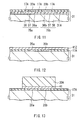
FIG. 11 is an enlarged cross section showing a process in a method
of manufacturing the magnetic memory device illustrated in FIG. 1.
FIG. 12 is an enlarged cross section showing a process subsequent
to FIG. 11.
FIG. 13 is an enlarged cross section showing a process subsequent
to FIG. 12
FIG. 14 is an enlarged cross section showing a process subsequent
to FIG. 13.
FIG. 15 is an enlarged cross section showing a process subsequent
to FIG. 14.
FIG. 16 is an enlarged cross section showing a process subsequent
to FIG. 15.
FIG. 17 is an enlarged cross section showing a process subsequent
to FIG. 16.
FIG. 18 is an enlarged cross section showing a process subsequent
to FIG. 17.
FIG. 19 is an enlarged cross section showing a process subsequent
to FIG. 18.
FIG. 20 is an enlarged cross section showing a process subsequent
to FIG. 19.
FIG. 21 is an enlarged cross section showing a process subsequent
to FIG. 20.
FIG. 22 is an enlarged cross section showing a process subsequent
to FIG. 21.
FIG. 23 is an enlarged cross section showing a process subsequent
to FIG. 22.
FIG. 24 is an enlarged cross section showing a process subsequent
to FIG. 23.
FIG. 25 is an enlarged cross section showing a process subsequent
to FIG. 24.
FIG. 26 is an enlarged cross section showing a process subsequent
to FIG. 25.
FIG. 27 is an enlarged cross section showing a process subsequent
to FIG. 26.
FIGs. 28A and 28B are diagrams illustrating shape characteristics
of a film to be patterned by a frame plating method applied as a part of the
method of manufacturing the memory cell shown in FIGs. 5A and 5B.
FIG. 29 is a characteristic diagram showing the relation between
the thickness of a pillar yoke in the memory cell illustrated in FIG. 5 and
switching current.
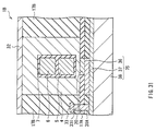
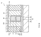
FIG. 30 is a cross section showing a first modification of the
memory cell illustrated in FIG. 7.
FIG. 31 is a cross section showing a second modification of the
memory cell illustrated in FIG. 7.
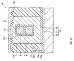
FIG. 32 is a cross section showing a third modification of the
memory cell illustrated in FIG. 7.
FIG. 33 is a cross section showing a fourth modification of the
memory cell illustrated in FIG. 7.
FIG. 34 is a cross section showing a fifth modification of the
memory cell illustrated in FIG. 7.
FIG. 35 is a circuit diagram showing another circuit configuration
of the magnetic memory device illustrated in FIG. 1.
FIG. 36 is a partial enlarged view of the circuit configuration
shown in FIG. 35.
DETAILED DESCRIPTION OF THE PRFERRED EMBODIMENTS
Embodiments of the invention will now be described in detail
hereinbelow with reference to the drawings.
First, with. reference to FIGs. 1 to 7, the configuration of a
magnetic memory device according to an embodiment of the invention will
be described.
FIG. 1 is a conceptual diagram showing a general configuration of
a magnetic memory device in the embodiment. The magnetic memory
device has an address buffer 51, a data buffer 52, a control logic part 53, a
memory cell group 54, a first drive control circuit part 56, a second drive
control circuit part 58, external address input terminals A0 to A20, and
external data terminals D0 to D7.
The memory cell group 54 has a matrix structure in which a
number of memory cells 1 each having a pair of tunneling
magneto-resistive elements (hereinbelow, called TMR elements) are
arranged in a word line direction (X direction) and a bit line direction (Y
direction) which are orthogonal to each other. The memory cell 1 is the
minimum unit for storing data in the magnetic memory device and is a
concrete example corresponding to a "magnetic memory cell" in the
invention. The memory cell 1 will be described in detail later.
The first drive control circuit part 56 has an address decoder
circuit 56A, a sense amplification circuit 56B, and a current drive circuit
56C in the Y direction. The second drive control circuit part 58 has an
address decoder circuit 58A, a constant current circuit 58B, and a current
drive circuit 58C in the X direction.
The address decoder circuits 56A and 58A are to select a word
decode line 72 (which will be described later) and a bit decode line 71
(which will be described later) according to an input address signal. The
sense amplification circuit 56B and the constant current circuit 58B are
circuits driven at the time of performing reading operation. The current
drive circuits 56C and 58C are circuits driven at the time of performing
writing operation.
The sense amplification circuit 56B and the memory cell group 54
are connected to each other via a plurality of bit decode lines 71 in which
the sense current flows at the time of reading operation. Similarly, the
constant current circuit 58B and the memory cell group 54 are connected to
each other via a plurality of word decode lines 72 in which the sense
current flows at the time of reading operation.
The Y-direction current drive circuit 56C and the memory cell
group 54 are connected to each other via write bit lines 5 (which will be
described later) necessary at the time of writing operation. Similarly, the
X-direction current drive circuit 58C and the memory cell group 54 are
connected to each other via write word lines 6 (which will be described
later) necessary at the time of writing operation.
The address buffer 51 has the external address input terminals A0
to A20 and is connected to the Y-direction address decoder circuit 56A in
the first drive control circuit part 56 and the X-direction address decoder
circuit 58A in the second drive control circuit part 58 via a Y-direction
address line 57 and an X-direction address line 55. The address buffer 51
receives an address signal from the outside via the external address input
terminals A0 to A20 and amplifies the address signal to a voltage level
required in the Y-direction address decoder circuit 56A and the X-direction
address decoder circuit 58B by a buffer amplifier (not shown) provided in
the address buffer 51. Further, the address buffer 51 functions to divide
the amplified address signal into two signals and output the signals to the
Y-direction address decoder circuit 56A via the Y-direction address line 57
and the X-direction address decoder circuit 58A via the X-direction address
line 55.
The data buffer 52 is constructed by an input buffer 52A and an
output buffer 52B, has the external data terminals D0 to D7, is connected
to the control logic part 53, and operates by an output control signal 53A
from the control logic part 53. The input buffer 52A is connected to the
Y-direction current drive circuit 56C in the first drive control circuit part
56 and the X-direction current drive circuit 58C in the second drive control
circuit part 58 via a Y-direction write data bus 61 and an X-direction write
data bus 60, respectively. At the time of performing an operation of
writing data to the memory cell group 54, the input buffer 52A functions to
receive signal voltages of the external data terminals D0 to D7, amplify the
signal voltage to a required voltage level by an internal buffer amplifier
(not shown), and transmit the resultant voltage to the X-direction current
drive circuit 58C and the Y-direction current drive circuit 56C via the
X-direction write data bus 60 and the Y-direction write data bus 61,
respectively. The output buffer 52B is connected to the sense
amplification circuit 56B via a Y-direction read data bus 62. At the time
of reading an information signal stored in the memory cell group 54, the
output buffer 52B functions to amplify the information signal supplied
from the sense amplification circuit 56B and to output the resultant signal
with a low impedance to the external data terminals D0 to D7.
The control logic part 53 has a chip select terminal CS and a write
enable terminal WE and is connected to the data buffer 52. The control
logic part 53 functions to receive a signal voltage from the chip select
terminal CS for selecting a memory cell to be read/written from the group
54 of plural memory cells and a signal voltage from the write enable
terminal WE for outputting a write permit signal and to output the output
control signal 53A to the data buffer 52.
The configuration related to information writing operation in the
magnetic memory device of the embodiment will now be described.
FIG. 2 is a conceptual diagram showing a configuration in plan
view of a main part related to the writing operation in the memory cell
group 54. As shown in FIG. 2, the magnetic memory device of the
embodiment includes a plurality of write bit lines 5a and 5b and the
plurality of write word lines 6 extending so as to cross the plurality of write
bit lines 5a and 5b. Each region in which the write bit lines 5a and 5b and
the write word line 6 cross each other includes a parallel part 10 in which
the write bit lines 5a and 5b and the write word line 6 extend parallel with
each other. Concretely, as shown in FIG. 2, the write word lines 6 extend
in the X direction in a rectangular wave shape and the write bit lines 5a
and 5b extend in the Y direction alternately and linearly. The rising and
falling portions of the rectangular wave shape of the write word lines 6
form the plurality of parallel parts 10 in cooperation with the write bit
lines 5a and 5b. The memory cell 1 is provided in the region where the
write bit lines 5a and 5b cross the write word line 6 so as to include at least
a part of the parallel part 10. The configuration that the memory cell 1 is
provided in the crossing region includes a case where the memory cell 1 is
provided next to the intersecting point. The memory cell 1 is constructed
by TMR elements 1a and 1b, the TMR element 1a is provided in a region
where the write bit line 5a and the write word line 6 cross each other, and
the other TMR element 1b is provided in the region where the write bit line
5b and the write word line 6 cross each other. The TMR elements 1a and
1b are a concrete example of "a pair of magneto-resistive elements" of the
invention.
To the write bit lines 5a and 5b and the write word line 6, currents
from the Y-direction current drive circuit 56C and the X-direction current
drive circuit 58C flow. The currents flowing in the write bit lines 5a and
the currents flowing in the write bit lines 5b are always in the opposite
directions. For example, as shown by the arrows in FIG. 2, when the
current directions in the write bit lines 5a are set as +Y direction, the
current directions in the write bit lines 5b are -Y direction. Therefore, in
this case, when the current directions in the write word lines 6 are set as
+X direction as a whole (from left to right in the drawing sheet), the
current directions of the write bit lines 5a and those of the write word lines
6 in the TMR elements 1a are parallel with each other. The current
directions of the write bit lines 5b and those of the write word lines 6
flowing in the other TMR elements 1b are also parallel with each other.
In the following, if it is unnecessary to discriminate the current directions
from each other, the write bit lines 5a and 5b will be simply referred to as
the write bit line 5. The write word line 6 is a concrete example
corresponding to a "first write line" in the invention, and the write bit line
5 is a concrete example corresponding to a "second write line" of the
invention.
FIG. 3 shows the configuration in plan view of the main part of the
memory cell group 54 more specifically. The write bit lines 5a and 5b,
write word lines 6, and memory cells 1 ( TMR elements 1a and 1b) shown in
FIG. 3 correspond to those in FIG. 2. The TMR elements 1a and 1b are
disposed in the parallel parts 10 of the write bit lines 5a and 5b and the
write word lines 6 in the Y direction. The TMR elements 1a and 1b have
stacked bodies S20a and S20b each including a magneto-sensitive layer
and the magnetic yokes 4a and 4b, respectively, and the magnetization
direction of the magneto-sensitive layer changes according to the magnetic
field generated by the currents flowing in the write bit line 5 and the write
word line 6 in the parallel part 10 (that is, the external magnetic field in
the magnetic yokes 4a and 4b). In this case, the write bit line 5 and the
write word line 6 in the parallel part 10 are provided in almost matched
positions in the XY plane. In the Z direction, they are disposed with a
predetermined interval and are electrically insulated from each other.
At both ends of the write bit line 5, write bit line lead electrodes 47
are provided. One of the write bit line lead electrodes 47 is connected to
the Y-direction current drive circuit 56C and the other one is connected so
as to be finally grounded. Similarly, write word line lead electrodes 46 are
provided at both ends of each write word line 6. One of the write word
line lead electrodes 46 is connected to the X-direction current drive circuit
58C and the other one is connected so as to be finally grounded. In FIG. 3,
the write bit lines 5 are partially omitted so that the shape of the write
word lines 6 can be seen well.
FIG. 4 is an enlarged perspective view of the memory cell 1. As
shown in FIG. 4, the write word line 6 and write bit lines 5a and 5b and
magnetic yokes 4a and 4b are electrically insulated from each other via
insulating films 7a and 7b. A stacked part 20b as a part of the stacked
body S20b is formed on the surface of the magnetic yoke 4b on the side
opposite to the write bit line 5b over the write word line 6. A read word
line 32 is provided so as to extend in the X direction on the side opposite to
the side where the stacked part 20b is formed in the magnetic yoke 4b.
Although not shown in FIG. 4, a stacked part 20a as a part of the stacked
body S20a corresponding to the write bit line 5a and the write word line 6
is formed on the surface of the magnetic yoke 4a a part of which is
commonly used by the magnetic yoke 4b. The pair of stacked bodies S20a
and S20b are connected to conductive layers 36a and 36b formed on the
side opposite to the magnetic yokes 4a and 4b (only the conductive layer
36b is shown). The pair of conductive layers 36a and 36b is a part of a
pair of Schottky diodes 75a and 75b (which will be described later) and the
other ends of the Schottky diodes 75a and 75b are connected to the read bit
lines 33a and 33b (not shown) extending in the Y direction.
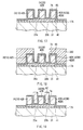
FIG. 5A shows a sectional configuration taken along line V-V of
the memory cell 1 illustrated in FIG. 3. FIG. 5B shows the memory cell 1
of FIG. 5A which is conceptually divided into the TMR element 1a and the
TMR element 1b.
As shown in FIGs. 5A and 5B, the TMR element 1a in the memory
cell 1 has: the magnetic yoke 4a disposed in correspondence with the area
where the write bit line 5a and the write word line 6 cross each other and
is constructed so as to surround the whole periphery of the write bit line 5a
and the write word line 6; and the stacked body S20a including the
magneto-sensitive layer of which magnetization direction changes
according to an external magnetic field, magnetically coupled to the
magnetic yoke 4a, and constructed so that current flows in the direction
perpendicular to the stacked face. The other TMR element 1b has: the
magnetic yoke 4b disposed in correspondence with the area where the write
bit line 5b and the write word line 6 cross each other and constructed so as
to surround the whole periphery of the write bit line 5b and the write word
line 6; and the stacked body S20b including the magneto-sensitive layer of
which magnetization direction changes according to an external magnetic
field, is magnetically coupled to the magnetic yoke 4b, and constructed so
that current flows in the direction perpendicular to the stacked face. The
TMR elements 1a and 1b share a common portion 34 as a part of the
magnetic yokes 4a and 4b. At least a part of the magnetic yoke 4 and one
of the write bit line 5 and the write word line 6 is made by a plating film.
The magneto-resistive layer is constructed by connection parts 14a
and 14b as a part of the magnetic yokes 4a and 4b and second magnetic
layers 8a and 8b which will be described later, respectively. The
connection parts 14a and 14b and the second magnetic layers 8a and 8b are
magnetically exchange-coupled to each other.
The stacked bodies S20a and S20b are constructed by the stacked
parts 20a and 20b and the connection parts 14a and 14b, respectively.
The stacked parts 20a and 20b are TMR films including, in order from the
side of the magnetic yokes 4a and 4b ( connection parts 14a and 14b), the
second magnetic layers 8a and 8b, tunnel barrier layers 3a and 3b, and
first magnetic layers 2a and 2b whose magnetization direction is fixed and
constructed so that current flows in the direction perpendicular to the
stacked face. As described above, the second magnetic layers 8a and 8b
function as the magneto-sensitive layers together with the connection parts
14a and 14b of the magnetic yokes 4a and 4b. In FIG. 5A, to clarify the
configuration of the stacked bodies S20a and S20b, the stacked bodies S20a
and S20b are exaggerated so as to be larger relative to the peripheral
parts.
When the magnetization directions of the pair of TMR elements 1a
and 1b are inverted in the directions which are not parallel with each other,
in the common portion 34, the directions of the current magnetic fields
generated by the write bit lines 5a and 5b and the write word line 6 become
the same and the magnetic flux density increases. Consequently, the
current magnetic field can be used more efficiently, and the current
necessary to invert the magnetization directions of the connection parts
14a and 14b of the magnetic yokes 4a and 4b and the second magnetic
layers 8a and 8b can be further decreased. Since the magnetic yoke 4 is
shared, the pair of TMR elements 1a and 1b can be easily formed, the
formation area of the memory cell 1 can be reduced, and capacity of stored
information can be increased.
In the stacked bodies S20a and S20b, when a voltage is applied in
the direction perpendicular to the stacked face between the first magnetic
layers 2a and 2b and the second magnetic layers 8a and 8b, for example,
electrons in the first magnetic layers 2a and 2b pass through the tunnel
barrier layers 3a and 3b and move to the second magnetic layers 8a and 8b,
and tunnel current flows. The tunnel current changes according to a
relative angle between the spin in the first magnetic layers 2a and 2b in
the interface with the tunnel barrier layer 3 and the spin in the second
magnetic layers 8a and 8b. Specifically, when the spin of the first
magnetic layers 2a and 2b and that of the second magnetic layers 8a and
8b are parallel with each other, the resistance value becomes the minimum.
When they are not parallel with each other, the resistance value becomes
the maximum. By using the resistance values, the magneto-resistance
change ratio (MR ratio) is defined as Equation (1).
MR ratio = dR/R
where "dR" denotes the difference between the resistance value in
the case where the spins are parallel with each other and that in the case
where the spins are not parallel with each other, and "R" indicates the
resistance value in the case where the spins are parallel with each other.
The resistance value against the tunnel current (hereinbelow,
called tunnel resistance Rt) strongly depends on the thickness T of the
tunnel barrier layer 3. In a low voltage region, as shown in Equation (2),
the tunnel resistance Rt exponentially increases with the thickness T of the
tunnel barrier layer 3.
Rt∝exp(2χT),χ = {8π2m*( · Ef)0.5}/h
where denotes the height of the barrier, "m*" denotes effective
mass of electrons, "Ef" indicates Fermi energy, and h indicates a blank
constant. Generally, in a memory element using the TMR element, to
match with a semiconductor device such as a transistor, it is said that the
proper tunnel resistance Rt is about 10 kΩ · (µm)2. However, to realize
higher packing density in the magnetic memory device and higher
operating speed, the tunnel resistance Rt is set to, preferably, 10 kΩ · (µm)2
or less, more preferably, 1kΩ · (µm)2 or less. Therefore, to realize the
tunnel resistance Rt, it is desirable to set the thickness T of the tunnel
barrier layer 3 to 2 nm or less, more preferably, 1.5 nm or less.
By reducing the thickness T of the tunnel barrier layers 3a and 3b,
the tunnel resistance Rt can be reduced and, on the other hand, a leak
current occurs due to roughness of the junction interface between the first
magnetic layers 2a and 2b and the second magnetic layers 8a and 8b so
that the MR ratio deteriorates. To prevent this, the thickness T of the
tunnel barrier layers 3a and 3b has to be large to an extent that leak
current does not flow. Concretely, the thickness T is desirably 0.3 nm or
larger.
Desirably, the stacked bodies S20a and S20b have a coercive force
difference type structure and the coercive force of the first magnetic layers
2a and 2b is larger than that of the second magnetic layers 8a and 8b.
Concretely, the coercive force of the first magnetic layer 2 is preferably
larger than (50/4π)×103A/m , more preferably, (100/4π)×103 A/m. With the
configuration, the magnetization direction of the first magnetic layers 2a
and 2b can be prevented from being influenced by unnecessary magnetic
fields such as external scattered magnetic fields or the like. The first
magnetic layers 2a and 2b are made of, for example, cobalt iron alloy
(CoFe) and have a thickness of 5 nm. Alternately, cobalt (Co), cobalt
platinum alloy (CoPt), nickel iron cobalt alloy (NiFeCo), or the like can be
applied to the first magnetic layers 2a and 2b. The second magnetic
layers 8a and 8b are made of, for example, cobalt (Co), cobalt iron alloy
(CoFe), cobalt platinum alloy (CoPt), nickel iron alloy (NiFe), or nickel iron
cobalt alloy (NiFeCo). The axes of easy magnetization of the first
magnetic layers 2a and 2b and the second magnetic layers 8a and 8b are
preferably parallel with each other so that the magnetization direction of
the first magnetic layers 2a and 2b and that of the second magnetic layers
8a and 8b are stabilized in a parallel or non-parallel state.
The magnetic yokes 4a and 4b extend so as to annularly surround
at least a part of the parallel part 10 in the write bit line 5 and the write
word line 6 and are constructed so that a return magnetic field is generated
in the magnetic yokes 4a and 4b by current flowing in the parallel part 10.
More specifically, as shown in FIG. 5B, the magnetic yoke 4a includes a
pair of pillar yokes 421 and 422 extending in the growth direction (Z
direction) of the plating film while facing each other, and a bottom yoke
41a and a top yoke 43a as a pair of beam yokes connecting with lower and
upper ends of the pillar yokes 421 and 422. The magnetic yoke 4a has a
closed sectional shape. The other magnetic yoke 4b includes a pair of
pillar yokes 422 and 423 extending in the growth direction (Z direction) of
the plating film while facing each other, and a bottom yoke 41b and a top
yoke 43b as a pair of beam yokes connecting with lower and upper ends of
the pillar yokes 422 and 423. The magnetic yoke 4b also has a closed
sectional shape. The TMR elements 1a and 1b share the pillar yoke 422, a
part of the bottom yokes 41a and 41b, and a part of the top yokes 43a and
43b and has the common portion 34 as shown in FIG. 5A. Each of the
magnetization directions of such yokes 4a and 4b is inverted by the return
magnetic field. In this case, the connection parts 14a and 14b of the
magnetic yokes 4a and 4b and the second magnetic layers 8a and 8b
adjacent to the connection parts 14a and 14b function as storage layers for
storing information. The magnetic yokes 4a and 4b are made of, for
example, nickel iron alloy (NiFe) and a part of the magnetic yokes 4a and
4b is made by a plating film. Consequently, the magnetic yokes 4a and 4b
have high dimensional precision and sufficient thickness. Preferably, the
coercive force of the connection parts 14a and 14b is smaller than that of
the first magnetic layers 2a and 2b within the range of (100/4π)×103A/m or
less for the following reason. When the coercive force exceeds
(100/4π)×103A/m, there is the possibility that the stacked parts 20a and 20b
themselves as the TMR films deteriorate due to heat generation caused by
increase in write current. Further, when the coercive force of the
connection parts 14a and 14b is equal to or larger than that of the first
magnetic layers 2a and 2b, the write current increases, the magnetization
direction of the first magnetic layers 2a and 2b as the magnetization fixed
layer changes, and the stacked parts 20a and 20b as storage elements are
destroyed. To make the current electric fields by the write bit lines 5a and
5b and the write word line 6 concentrated on the magnetic yokes 4a and 4b,
the magnetic permeability of the magnetic yokes 4a and 4b is preferably
high. Concretely, the magnetic permeability is preferably 2000 or higher
and, more preferably, 6000 or higher.
Each of the write bit line 5 and the write word line 6 has a
structure in which a film of titanium (Ti) having a thickness of 10 nm, a
film of titanium nitride (TiN) having a thickness of 10 nm, and a film of
aluminum (Al) having a thickness of 500 nm are sequentially stacked and
are electrically insulated from each other via the insulating films 7. The
write bit line 5 and the write word line 6 may be made of at least one of, for
example, aluminum (Al), copper (Cu), and tungsten (W). A more concrete
operation of writing information to the memory cell 1 by using the write bit
line 5 and the write word line 6 will be described later.
The configuration related to information reading operation will
now be described. FIG. 6 is a plan view showing the configuration of a
main part related to the reading operation of the memory cell group 54 and
corresponds to FIG. 3.
As shown in FIG. 6, each memory cell 1 is disposed at each of the
intersecting points of the plurality of read word lines 32 and the plurality
of read bit lines 33 in the XY plane. The stacked parts 20a and 20b on the
under face of the memory cell 1 are connected to a pair of read bit lines 33a
and 33b via the Schottky diodes 75a and 75b, and the top face (the side
opposite to the stacked parts 20a and 20b) is in contact with the read word
line 32. The read bit lines 33a and 33b supply read current to the pair of
TMR elements 1a and 1b in each memory cell 1 and the read word line 32
leads the read current passed to the TMR elements 1a and 1b to the ground.
At both ends of each read bit line 33, read bit line lead electrodes 49 are
provided. At both ends of each read word line 32, read bit line lead
electrodes 48 are provided.
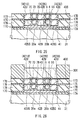
FIG. 7 is a cross section taken along line VII-VII of FIG. 6. As
shown in FIG. 7, a magnetic memory device of the embodiment is
constructed so that, in a region including the memory cell 1, a pair of
stacked parts 20a and 20b and the magnetic yokes 4a and 4b are
sequentially formed on a substrate 31 provided with the Schottky diode 75
(hereinbelow, simply called diode 75) functioning as a rectifier.
The pair of diodes 75a and 75b have the conductive layers 36a and
36b, an epitaxial layer 37, and a substrate 38 in order from the side of the
stacked parts 20a and 20b. Between the conductive layers 36a and 36b
and the epitaxial layer 37, a Schottky barrier is formed. The diodes 75a
and 75b do not have an electrically connected part except for connection to
the annular magnetic layer 4 while sandwiching the stacked parts 20a and
20b. The substrate 38 is an n-type silicon wafer. Generally, in the n-type
silicon wafer, an impurity of phosphorus (P) is diffused. As the substrate
38, a wafer of an n++ type obtained by being highly doped with phosphorus
is used. As the epitaxial layer 37, a wafer of the n type obtained by being
lightly doped with phosphorus is used. By making the epitaxial layer 37
as an n-type semiconductor and the conductive layers 36a and 36b made of
a metal come into contact with each other, a band gap is created and a
Schottky barrier is formed. Further, the pair of diodes 75a and 75b are
connected to the read bit lines 33a and 33b, respectively, via a connection
layer 33T.
Referring now to FIG. 8, the circuit configuration related to the
reading operation in the magnetic memory device of the embodiment will
be described.
FIG. 8 is a configuration diagram of a circuit system constructed
by the memory cell group 54 and a read circuit. In the read circuit system,
the memory cell 1 is of a differential amplifier type constructed by the pair
of TMR elements 1a and 1b. Information in the memory cell 1 is read by
outputting a differential value of read currents passed to the TMR
elements 1a and 1b (currents passed from the read bit lines 33a and 33b to
the TMR elements 1a and 1b, respectively, and output to the common read
word line 32).
In FIG. 8, a unit read circuit 80 (..., 80n, 80n+1, ...) as a unit of
repetition of the read circuit is constructed by the memory cells 1 of each
bit line in the memory cell group 54 and a part of the read circuit including
the sense amplification circuit 56B, and the unit read circuits 80n are
arranged in the bit line direction. Each of the unit read circuits 80n is
connected to the Y-direction address decoder circuit 56A via the bit decode
line 71 (..., 71n, 71n+1, ...) and is connected to the output buffer 52B via
the Y-direction read data bus 62.
In the memory cell group 54, the read word lines 32 (..., 32m,
32m+1, ...) arranged in the X direction and the pair of read bit lines 33a
and 33b arranged in the Y direction are disposed in a matrix. Each of the
memory cells 1 is disposed at the intersecting position with the read word
line 32 in a region sandwiched by the pair of read bit lines 33a and 33b.
Ends of each of the TMR elements 1a and 1b in each memory cell 1 are
connected to the read bit lines 33a and 33b via the pair of diodes 75a and
75b and the other ends are connected to the common read word line 32.
One end of each read word line 32 is connected to a read switch 83
(..., 83m, 83m+1, ...) via the read word line lead electrode 48 and is also
connected to a common constant current circuit 58B. Each read switch 83
is connected to the X-direction address decoder circuit 58A via the word
decode line 72 (..., 72m, 72m+1, ...). The read switch 83 is made conductive
when a selection signal from the X-direction address decoder circuit 58A is
supplied. The constant current circuit 58B has the function of making the
current flowing in the read word line 32 constant.
One end of each read bit line 33 is connected to the sense
amplification circuit 56B via the read bit line lead electrode 49, and the
other end is finally grounded. One sense amplification circuit 56B is
provided per unit read circuit 80 and has the function of receiving the
potential difference between the pair of read bit lines 33a and 33b in each
unit read circuit 80, and amplifying the potential difference. The sense
amplification circuit 56B is connected to the output line 82 (..., 82n, 82n+1,
...) and is finally connected to the output buffer 52B via the Y-direction
read data bus 62.
The operation in the magnetic memory device of the embodiment
will now be described.
Referring now to FIG. 2 and FIGs. 9A and 9B, the writing
operation in the memory cell 1 will be described. FIGs. 9A and 9B express
the relation between the write current direction and the return magnetic
field direction (magnetization direction) in the sectional configuration of
the memory cell 1 shown in FIG. 5. The arrows indicated in magnetic
layers in FIGs. 9A and 9B indicate the magnetization directions of the
magnetic layers. With respect to the magnetic yokes 4a and 4b, the
magnetic field directions of a magnetic path formed on the inside are also
shown. The magnetization of the first magnetic layers 2a and 2b is fixed
to the -X direction. FIGs. 9A and 9B show the case where write current
flows in the same direction to the write bit line 5 and the write word line 6
which extend in the memory cell 1 and are parallel with each other. FIG.
9A corresponds to the write current direction shown in FIG. 2. FIG. 9A
shows a case where write current flows from this side to the depth in the
direction perpendicular to the drawing sheet (to the +Y direction) in the
TMR element 1a, a return magnetic field 16a is generated in the clockwise
direction in the potion of magnetic yoke 4a, which surrounds the write bit
line 5a, write current flows from the depth to this side in the direction
perpendicular to the drawing sheet (to the -Y direction) in the TMR
element 1b, and the return magnetic field 16b is generated in the
counterclockwise direction in the portion of magnetic yoke 4b, which
surrounds the write bit line 5b. In this case, the magnetization direction
of the connection part 14a and the second magnetic layer 8a becomes the
- X direction and the magnetization direction of the connection part 14b
and the second magnetic layer 8b becomes the +X direction. FIG. 9B
corresponds to the case where the directions of current flowing in the write
bit line 5 and the write word line 6 are opposite to those shown in FIG. 9A.
Specifically, FIG. 9B shows a case where write current flows from the
depth to this side in the direction perpendicular to the drawing sheet (to
the -Y direction) in the TMR element 1a, the return magnetic field 16a is
generated in the counterclockwise direction in the portion of magnetic yoke
4a, which surrounds the write bit line 5a, write current flows from this side
to the depth in the direction perpendicular to the drawing sheet (to the +Y
direction) in the TMR element 1b, and the return magnetic field 16b is
generated in the clockwise direction in the magnetic yoke 4b of the portion
surrounding the write bit line 5b. In this case, the magnetization
direction of the connection part 14a and the second magnetic layer 8a is the
+X direction and the magnetization direction of the connection part 14b
and the second magnetic layer 8b is the -X direction.
In the cases of FIGs. 9A and 9B, the current direction of the write
bit line 5a and the write word line 6 penetrating the TMR element 1a and
that of the write bit line 5b and the write word line 6 penetrating the TMR
element 1b are opposite to each other. Consequently, the directions of the
return magnetic fields 16a and 16b flowing in the pillar yoke 422 (refer to
FIG. 5) corresponding to the common part 34 of the magnetic yokes 4a and
4b can be made the same (the +Z direction in FIG. 9A and the -Z direction
in FIG. 9B).
As obvious from FIGs. 9A and 9B, according to the directions of
the return magnetic field 16a and 16b generated by the currents flowing in
the write bit line 5 and the write word line 6 penetrating the magnetic
yokes 4a and 4b, the magnetization direction of the connection part 14a
and the second magnetic layer 8a and that of the connection part 14b and
the second magnetic layer 8b change so as to be opposite to each other. By
using the phenomenon, information can be stored in the memory cell 1.
In short, when current flows in the same direction in the write bit
lines 5a and 5b and the write word line 6, the magnetization directions of
the magnetic yokes 4a and 4b are inverted and, accompanying the
inversion, the magnetization directions of the second magnetic layers 8a
and 8b change, thereby enabling binary information of "0" or "1" to be
stored. In the case where "0" corresponds to, for example, the state of FIG.
9A, specifically, the state where the connection part 14a and the second
magnetic layer 8a are magnetized in the -X direction and the other
connection part 14b and the second magnetic layer 8b are magnetized in
the +X direction, "1" corresponds to the state of FIG. 9B, specifically, the
state where the connection part 14a and the second magnetic layer 8a are
magnetized in the +X direction and the other connection part 14b and the
second magnetic layer 8b are magnetized in the -X direction. In such a
manner, information can be stored.
In this case, in the TMR elements 1a and 1b, when the
magnetization direction of the first magnetic layers 2a and 2b and that of
the second magnetic layers 8a and 8b are parallel with each other, a low
resistance state in which large tunnel current flows is obtained. When
they are not parallel with each other, a high resistance state in which only
small tunnel current flows is obtained. That is, one of the pair of TMR
elements 1a and 1b is in the low resistance state and the other is in the
high resistance state, thereby storing information. In the case where the
write currents flow in the opposite directions in the write bit line 5 and the
write word line 6 or in the case where the write current flows only in one of
the write bit line 5 and the write word line 6, the magnetization direction
of the second magnetic layer 8 is not inverted and the data is not rewritten.
As described above, in the memory cell 1 in the magnetic memory
device of the embodiment having the configuration, by passing the currents
in the same direction to both of the write bit line 5 and the write word line
6, the direction of the current magnetic field generated by the write bit line
5 and that of the current magnetic field generated by the write word line 6
become the same in the magnetic yoke 4, so that a synthetic magnetic field
can be generated. Consequently, as compared with the case where the
magnetic yoke 4 is not provided and the case where the write bit line 5 and
the write word line 6 perpendicularly cross each other, higher magnetic
flux density is obtained. Thus, the current magnetic field can be used
more efficiently and the current necessary to invert the magnetization in
the connection part 14 of the magnetic yoke 4 and the second magnetic
layer 8 can be reduced.
Further, since the second magnetic layer 8 is provided between the
tunnel barrier layer 3 and the connection part 14 of the magnetic yoke 4,
the following advantages are obtained. Exchange coupling between the
connection part 14 and the second magnetic layer 8 can be formed and the
magnetization direction in the second magnetic layer 8 as the second
magneto-sensitive part is aligned more excellently, so that more stable
writing can be performed. Further, the coercive force of the connection
part 14 can be suppressed more, so that a heat generation amount can be
decreased by reducing the current value in the writing operation, and the
functions of the magnetic memory device can be fully displayed.
Referring now to FIGs. 1 and 8, the reading operation in the
magnetic memory device of the embodiment will be described.
First, one of the bit decode lines 71 is selected by the address
decoder circuit 56A in the first drive control circuit part 56 and a control
signal is transmitted to the corresponding sense amplification circuit 56B.
As a result, read current flows in the read bit lines 33a and 33b and the
positive potential is given to the side of the stacked bodies S20a and S20b
in the TMR elements 1a and 1b. Similarly, by the X-direction address
decoder circuit 58A in the second drive control circuit part 58, one of the
plurality of word decode lines 72 is selected and the read switch 83 in the
corresponding part is driven. The selected read switch 83 is made
conductive, read current flows in the corresponding read word line 32, and
a negative potential is given to the side opposite to that of the stacked
bodies S20a and S20b. Therefore, read current necessary for reading can
be passed to one memory cell 1 selected by the Y-direction address decoder
circuit 56A and the X-direction address decoder circuit 58A. Based on the
read current, the magnetization directions of the pair of second magnetic
layers 8a and 8b are detected, thereby enabling stored information to be
read.
FIGs. 10A and 10B are circuit diagrams each showing a portion
around the memory cell 1. The magnetization directions of the first
magnetic layers 2a and 2b in the stacked bodies S20a and S20b are
indicated by hollow arrows and those of the second magnetic layers 8a and
8b are indicated by solid arrows. Both of the magnetization directions of
the first magnetic layers 2a and 2b are fixed to the left directions. In FIG.
10A, the magnetization direction of the first magnetic layer 2a and that in
the second magnetic layer 2b in the stacked body S20a are the same, and
the magnetization direction of the first magnetic layer 2b and that of the
second magnetic layer 2b in the other stacked body S20b are opposite to
each other. In this case, the stacked body S20a is in the low resistance
state, and the stacked body S20b is in the high resistance state. This case
corresponds to, for example, "0". In the other case of FIG. 10B, different
from the case of FIG. 10A, the stacked body S20a is in the high resistance
state and the stacked body S20b is in the low resistance state. This case
corresponds to, for example, "1". Such binary information can be obtained
by detecting the difference between the current values due to the difference
between values of the stacked bodies S 20a and S20b.
In the magnetic memory device of the embodiment, with the
configuration as described above, by passing current to both of the write bit
line 5 and the write word line 6, a closed magnetic path can be formed, the
magnetization can be inverted efficiently in the magnetic yokes 4a and 4b
in the TMR elements 1a and 1b, and the magnetic influence on a memory
cell adjacent to the memory cell 1 to be written can be reduced. Since a
part of the magnetic yokes 4a and 4b, write bit lines 5a and 5b and the
write word line 6 are made by a plating film, the magnetic yokes 4a and 4b,
write bit lines 5a and 5b, and write word line 6 can assure high
dimensional precision and sufficient thickness. Consequently, a return
magnetic field sufficient to perform stable magnetization inversion can be
generated in the magnetic yoke 4 and the more stable writing and reading
operations can be performed. Further, by the shield effect of the magnetic
yokes 4a and 4b, the intervals of neighboring memory cells can be
narrowed on the substrate. Thus, it is advantageous for higher
integration and higher packing density of the magnetic memory device.
A method of manufacturing the magnetic memory cell having the
configuration as described in the embodiment and a method of
manufacturing the magnetic memory device having the configuration as
described in the embodiment will now be described.
In the methods of manufacturing the magnetic memory cell and
the magnetic memory device having the magnetic memory cell in the
embodiment, at least a part of the annular magnetic layer is formed by
plating. Hereinbelow, referring to FIGs. 11 to 27, the method of
manufacturing mainly the memory cell 1 in the magnetic memory device
will be concretely described. FIGs. 11 to 27 are cross sections
corresponding to FIG. 7 and show manufacturing processes in order.
In the first process, a bottom yoke 41 is formed on the substrate 31
via the stacked parts S20a and S20b. First, as shown in FIG. 11, the
substrate 31 in which the diodes 75a and 75b are buried and on which the
stacked parts S20a and S20b and the insulating film 17A surrounding the
periphery of the stacked parts S20a and S20b is prepared. In FIGs. 12 to
27 subsequent to FIG. 11, the details of the substrate 31 will be omitted.
Subsequently, as shown in FIG. 12, a metal film 41Z made of nickel iron
alloy (NiFe) is formed by, for example, sputtering on the entire surface.
After that, as shown in FIG. 13, a resist pattern 30A in a predetermined
shape is formed on the metal film 41Z of the region corresponding to the
stacked parts S20a and S20b. By removing the unnecessary metal film
41Z by milling or the like, the bottom yoke 41 (41a and 41b) is obtained.
Generally, such a thin film patterning method is called milling.
In the following second process, on the bottom yoke 41, three
bottom pillar yokes 42B (421B, 422B, and 423B) are formed. First, the
resist pattern 30A is removed and, as shown in FIG. 14, an underplating
film 42BS made of NiFe is formed on the entire surface by, for example,
sputtering. On the underplating film 42BS, a resist pattern 30B is
selectively formed. In this case, a region for forming the bottom pillar
yoke 42B is left. After that, the resultant is soaked in a plating solution
and a plating process using the underplating film 42BS as an electrode is
performed, thereby forming the three bottom pillar yokes 42B made of, for
example, NiFe as shown in FIG. 15. After forming the bottom pillar yokes
42B, the resist pattern 30B is peeled off, and the exposed underplating film
42BS is removed by milling or the like. Generally, such a thin film
patterning method is called a frame plating method.
In the following third process, the write word lines 6 are formed
between the bottom pillar yokes 42B via insulating films 7A. In this case,
first, as shown in FIG. 16, the insulating film 7A made of Al2O3 or the like
is formed so as to cover the whole by using, for example, a CVD apparatus.
After that, as shown in FIG. 17, an underplating film 6S made of, for
example, copper is formed so as to cover the insulating film 7A by
sputtering or the like. After that, as shown in FIG. 18, a resist pattern
30C is selectively formed so as to leave the region between the bottom
pillar yokes 42B. Further, as shown in FIG. 19, a metal layer 6Z is
formed so as to bury at least the regions between the bottom pillar yokes
42B. In this case, the resultant is soaked in a plating solution and a
plating process using the underplating film 6S as an electrode is performed,
thereby forming the metal layer 6Z made of copper. After that, the resist
pattern 30C is peeled off and the exposed underplating film 6S is removed
by milling or the like. Further, as shown in FIG. 20, an insulating film
17B made of, for example, Al2O3 is formed so as to cover the whole by
sputtering or the like. After that, as shown in FIG. 21, the whole face is
polished to a predetermined thickness so as to be planarized by using, for
example, a CMP apparatus. In such a manner, the write word line 6 is
formed.
In the following fourth process, an insulating film 7B is formed so
as to cover the top face of the write word line 6 and surround the periphery
of the write word line 6 in cooperation with the insulating film 7A.
Concretely, as shown in FIG. 22, a resist pattern 30D is selectively formed
in regions except for the region in which the write word line 6,
underplating film 6S, and insulating film 7A are exposed in the surface.
After that, the resist pattern 30D is used as a mask and sputtering is
performed, thereby forming the insulating film 7B made of, for example,
Al2O3 as shown in FIG. 23. Further, by removing the resist pattern 30D,
the insulating film 7B covering the write word line 6, underplating film 6S,
and the insulating film 7A appears. By forming an undercut in a lower
part of the end face of the resist pattern 30D, the resist pattern 30D can be
easily peeled off.
In a fifth process, three top pillar yokes 42U (421U, 422U, and
423U) are formed on the three bottom pillar yokes 42B (421B, 422B, and
423B). The top pillar yokes 42U can be formed by repeating an operation
similar to the process of forming the bottom pillar yokes 42B shown in
FIGs. 14 and 15. In a sixth process, the write bit lines 5 (5a and 5b) are
formed via the insulating film 7C between the top pillar yokes 42U. The
write bit lines 5 can be formed by repeating an operation similar to that of
forming the write word lines 6 shown in FIGs. 16 to 23. Further, in a
seventh process, an insulating film 7D is formed so as to cover the top face
of the write bit line 5 and surround the periphery of the write bit line 5 in
cooperation with the insulating film 7C. Hereinbelow, by referring to FIG.
24, the fifth to seventh processes will be described concretely.
In the fifth process, first, the insulating film 7B is formed in the
fourth process and, after that, an underplating film 42US made of NiFe is
formed on the entire face by, for example, sputtering. After that, a resist
pattern (not shown) is selectively formed on the underplating film 42US.
In this case, the region for forming the top pillar yoke 42U is left. The
resultant is soaked in a plating solution, and a plating process using the
underplating film 42US as an electrode is performed, thereby forming the
top pillar yoke 42U made of, for example, NiFe. After forming the top
pillar yoke 42U, the resist pattern is peeled off, and the exposed
underplating film 42US is removed by milling or the like. In the following
sixth process, an insulating film 7C made of Al2O3 or the like is formed so
as to cover the whole by using, for example, a CVD apparatus. After that,
the underplating film 5S made of, for example, copper is formed so as to
cover the insulating film 7C by sputtering or the like. A resist pattern
(not shown) is selectively formed so as to leave the regions between the top
pillar yokes 42U. Further, the write bit lines 5 are formed so as to bury
the region between the top pillar yokes 42U. In this case, the resultant is
soaked in a plating solution and a plating process using the underplating
film 5S as an electrode is performed, thereby forming the write bit line 5
made of copper: After formation of the write bit line 5, the resist pattern
is peeled off and the underplating film 5S is removed by milling or the like.
Further, an insulating film 17D made of, for example, Al2O3 is formed so as
to cover the whole by sputtering or the like. After that, the whole face is
polished to a predetermined thickness so as to be planarized by using, for
example, a CMP (Chemical Mechanical Polishing) apparatus. In the
following seventh process, a resist pattern (not shown) is selectively formed
in regions except for the region in which the write bit line 5, underplating
film 5S, and insulating film 7C are exposed in the surface. The resist
pattern is used as a mask and sputtering is performed, thereby forming the
insulating film 7D made of, for example, Al2O3. By removing the resist
pattern, the insulating film 7D covering the write bit line 5, underplating
film 5S, and the insulating film 7C appears.
In the following eighth process, by providing the top yoke 43 so as
to cover the top pillar yoke 42U and the insulating film 7D, formation of
the magnetic yoke 4 constructed by the bottom yoke 41, the pair of bottom
and top pillar-shaped magnetic layers 42B and 42U and the top yoke 43 is
completed. Concretely, first, as shown in FIG. 25, the underplating film
43S is formed so as to cover the whole by sputtering or the like. Next, as
shown in FIG. 26, a resist pattern 30E is selectively formed so as to avoid
the region corresponding to the formation region of the bottom yoke 41.
The resist pattern 30E is used as a mask and a plating process using the
underplating film 43S is performed, thereby forming the top yoke 43 made
of, for example, NiFe. After formation of the top yoke 43, the resist
pattern 30E is peeled off and the exposed underplating film 43S is removed
by milling or the like. Subsequently, an insulating film 17F made of Al2O3
or the like is formed on the whole face. As shown in FIG. 27, the whole
face is polished to a predetermined thickness by using, for example, a CMP
apparatus and planarized. The formation of the magnetic yoke 4 is
completed and the memory cell 1 is completed. Further, the read word
line 32 having a desired width is formed so as to be electrically connected
to the top yoke 43.
After that, the write word line lead electrodes 46 are formed at
both ends of the write word line 6, the write bit line lead electrodes 47 are
formed at both ends of the write bit line 5, the read word line lead
electrodes 48 are formed at both ends of the read word line 32 and, further,
the read bit line lead electrodes 49 are formed at both ends of the read bit
line 33.
In such a manner, formation of the memory cell group 54 including
the memory cells 1 is completed.
Further, by performing a process of forming a protection layer
made of silicon oxide (SiO2), Al2O3, or the like by a sputtering apparatus, a
CVD apparatus, or the like and a process of polishing the protection layer
to expose the lead electrodes 46 to 49, manufacture of the magnetic
memory device is completed.
As described above, in the embodiment, the bottom and top pillar
yokes 42 and top yokes 43 in the magnetic yoke 4, write bit line 5, and
write word line 6 are formed by plating. When they are formed by a dry
film forming method by sputtering or the like and a dry film forming
method combined with a dry patterning method such as milling, reactive
ion etching, or the like, the following problems occur. First, in the dry film
forming method such as sputtering, although it is easy to form a thin film
of a few nm or less, it is not suitable for reasons such that it takes time to
form a functional film having a thickness of hundreds nm. When a film to
be patterned is subjected to dry etching by using the resist pattern as a
mask, generally, the resist pattern itself is also etched and the film is
reduced not only in the thickness direction but also in the width direction
(in-plane direction). Moreover, the gradient of the end face of the film to
be patterned tends to become gentle. Consequently, it is difficult to obtain
high dimensional precision.
One of methods of making the gradient of the end face of the film
to be patterned sharp is a method of using an inorganic mask material
having a low etching rate (which is not easily etched). In this case,
however, the unnecessary inorganic mask material remains on the film to
be patterned, so that it is difficult to apply the method to the method of
manufacturing the magnetic memory device in the embodiment.
In contrast, in the manufacturing method of the embodiment, the
bottom and top pillar yokes 42, top yoke 43, write bit line 5 and write word
line 6 in the magnetic yoke 4 are formed by plating. Consequently, as
compared with the case where they are formed by a dry method such as
sputtering, a larger edge angle can be realized and the yoke 4, write bit
line 5 and write word line 6 can be formed with high precision and with
sufficient thickness. Consequently, neighboring memory cells can be
disposed at smaller intervals on the substrate, and the magnetic memory
device realizing higher integration and higher packing density can be
formed.
Examples
Concrete examples in the embodiment will now be described.
First, the inclination angle of the end face in the film to be
patterned which is made of NiFe and formed by the frame plating method
of the embodiment and that formed by the dry film forming method were
compared with each other. FIG. 28A shows the result.
The lateral axis in FIG. 28A indicates average thickness Tave.
(nm) of a film PF to be patterned, and the vertical axis indicates the
inclination angle (deg.) of the end face of the film PF to be patterned.
The inclination angle is, as shown in FIG. 28B, an angle formed by a
supporting face 131S on which the film PF to be patterned is formed and
the end face of the film PF to be patterned. When the inclination angle
is 0°, it means that the end face is parallel with the supporting face 131S.
When the inclination angle is 90°, it means that the end face is
perpendicular to the supporting face 131S. "○" shows the characteristic
value of a sample formed by the frame plating method, "▴" expresses the
characteristic value of a sample formed by the milling method, and ""
denotes the characteristic value of a sample formed by reactive ion etching
+(RIE). Samples with six kinds of thicknesses were prepared for each of
the methods and the edge angles were measured. The sample formed by
the frame plating method is a plating film pattern made of NiFe and
having a desired thickness, and was formed as follows. An electrode film
made of NiFe was formed by sputtering, a chemically amplified resist
pattern for 248 nm was selectively formed on the electrode film, the
resultant was soaked in a nickel Watt bath containing iron ions, and a
plating process was performed, thereby forming a plated film pattern.
Further, by using the plated film pattern as a mask, the electrode film was
removed by milling. In this case, the thickness of the electrode film was
about 30 nm. The chemically amplified resist pattern for 248 nm was
formed so that the plated film has a thickness of +50 nm and a trench
width of about 500 nm. The sample by the milling was formed as follows.
An NiFe film having a predetermined thickness was formed by sputtering.
A chemically amplified resist pattern for 248 nm having a thickness of 300
nm and a line width of 500 nm was selectively formed on the NiFe film.
By using the resist pattern as a mask, the NiFe film was subjected to
milling by using an argon gas in a direction perpendicular to the
supporting face. The parameters of the milling were a gas pressure of
2.67×10⁻² Pa, beam current of 300 mA, and acceleration voltage of -500V.
The sample by RIE was formed as follows. An NiFe film having a
predetermined thickness was formed by sputtering. On the NiFe film, a
titanium (Ti) film having a thickness of 50 nm and a width of 500 nm was
selectively formed. Further; the titanium film was used as a mask and
the NiFe film was etched by RIE, thereby forming the sample. The
apparatus was of a capacitive-coupling parallel flat electrode type. As
etching parameters, a gas obtained by mixing 50 mol% of NH3 and 50 mol%
of CO, in which a gas pressure is 0.75 Pa, frequency is 13.26 MHz, and
high-frequency power density is 4×10⁴W/cm2, was used.
As shown in FIG. 28A, the sample "○" formed by the frame plating
method maintains large inclination angles of the same extent (almost
90°) through the range of the thickness Tave. from 100 nm to 500 nm. On
the other hand, the sample "▴" formed by milling and the sample ""
formed by RIE have the inclination angles which decrease as the
thickness Tave. increases, that is, the inclination of the end face is gentle.
In particular, in the sample shown by "" and formed by RIE, decrease in
the inclination angle is conspicuous. At the thickness Tave. of 500 nm,
the inclination angle is about 20°. From the results, it was found that
by forming the film to be patterned made of NiFe by the frame plating
method, the end face can be formed almost perpendicular to the supporting
face. Therefore, by applying the method to the method of manufacturing
the magnetic memory device, higher integration and higher packing
density can be achieved.
The relation between the pillar yoke having the sectional structure
shown in FIG. 5A in the embodiment and the switching current in the
magnetic memory cell was examined. FIG. 29 shows the result.
FIG. 29 shows the result of measuring the write current of a
magnitude necessary to invert the magnetization direction in the
magneto-sensitive layer (the connection part 14a and the second magnetic
layer 8a) of the TMR element 1a and the magneto-sensitive layer (the
connection part 14b and the second magnetic layer 8b) of the TMR element
1b shown in FIG. 5A, that is, the switching current. The lateral axis
indicates the length in the Z direction of the pillar yoke 42, that is, the
thickness (nm). The vertical axis indicates the switching current (mA) of
a magnitude necessary to invert the magnetization direction. In FIG. 29,
the plot shown by "○" indicates the switching current necessary to invert
the magnetization of the magneto-sensitive layer of the TMR element 1a
and the plot shown by "" indicates the switching current necessary to
invert the magnetization of the magneto-sensitive layer of the TMR
element 1b. When the thickness is 400 nm, the switching current of 1.2
mA is passed in both of the cases. As the thickness decreases, the
difference between the cases increases. In particular, when the thickness
is 200 nm, the switching current in the magneto-sensitive layer in the TMR
element 1b becomes 1.0 mA which is a smaller value. The switching
current in the magneto-sensitive layer of the TMR element 1a is 1.9 mA
which is almost twice as large as that of the TMR element 1b.
In the memory cell 1 shown in FIG. 5A, the magnetization
direction of the magneto-sensitive layer in the TMR element 1a and that in
the magneto-sensitive layer in the TMR element 1b are made opposite to
each other, thereby recording information. Therefore, in a state where the
magnetization of only one of the magneto-sensitive layers is inverted,
information is not recorded. As shown in FIG. 29, when the thickness of
the pillar yoke 42 is 200 nm, although by setting the switching current to
1.0 mA, the magnetization direction of the magneto-sensitive layer of the
TMR element 1b is inverted, the magnetization direction of the
magneto-sensitive layer of the TMR element 1a is not inverted. Therefore,
information cannot be recorded. In this case, by setting the switching
current to 1.9 mA or larger, both of the magnetization directions of the
magneto-sensitive layers of the TMR elements 1a and 1b can be inverted.
In the case where the thickness of the pillar yoke 42 is 300 nm, by setting
the switching current to 1.3 mA or larger, both of the magnetization
directions of the magneto-sensitive layers of the TMR elements 1a and 1b
can be inverted. Further, when the thickness of the pillar yoke 42 is 400
nm, by setting the switching current to 1.2 mA or larger, both of the
magnetization directions of the magneto-sensitive layers of the TMR
elements 1a and 1b can be inverted. It is considered that by increasing
the thickness of the pillar yoke 42, a uniform magnetic field of little
deviation in the horizontal direction is formed more easily in the yoke 4.
As described above, we could have confirmed that the switching
current depends on the thickness of the pillar yoke and, by increasing the
thickness of the pillar yoke, the difference between the switching currents
in the magneto-sensitive layers of the TMR elements 1a and 1b can be
reduced and both of the magnetization directions of the TMR elements 1a
and 1b can be inverted even by a lower switching current, so that it is
efficient.
Although the invention has been described above in the
embodiment and examples, the invention is not limited to the embodiment
and examples but can be variously modified. Concretely, for example, in
the embodiment, the case where each of the pair of magneto-resistive
elements in the magnetic memory cell has an annular magnetic yoke and
the pair of annular magnetic yokes are connected to each other has been
described. The invention is not limited to the case. For example, like a
memory cell 1A (first modification) shown in FIG. 30, two magnetic yokes
each having a U shape of which opening part is positioned opposite to that
of the stacked body (magnetic yokes each having a sectional shape a part of
which is open) may be coupled to each other. Concretely, the memory cell
1A shown in FIG. 30 has: the TMR element 1a including the bottom yoke
41a and the pair of pillar yokes 421 and 422 coupled to both ends of the
bottom yoke 41a and extending in the direction orthogonal to the
supporting face 31S; and the TMR element 1b including the bottom yoke
41b and the pair of pillar yokes 422 and 423 coupled to both ends of the
bottom yoke 41b and extending in the direction orthogonal to the
supporting face 31S. The pair of TMR elements 1a and 1b share at least
the pillar yoke 422. Also in such a configuration, by forming at least a
part of the magnetic yoke by the plating method, high dimensional
precision and sufficient thickness can be assured. Also in the case of
applying the method to the magnetic memory device, higher integration
and higher packing density can be achieved.
Although the magnetic memory cell having a pair of
magneto-resistive elements has been described in the foregoing
embodiment, the invention is not limited to the magnetic memory cell.
For example, like a memory cell 1B (second modification) shown in FIG. 31,
a single TMR element having one magnetic yoke 4 and one stacked part 20
may be used as a magnetic memory element. Also in the memory cell 1B
having such a configuration, by forming at least a part of the magnetic
yoke 4 by the plating method, high dimensional precision and sufficient
thickness can be assured. Also in the memory cell formed by a single
TMR element, like a memory cell 1C (third modification) shown in FIG. 32,
not an annular yoke but a magnetic yoke having a U shape in cross section
and a part of which is open may be provided. In particular, in the case of
a memory cell made by a single TMR element, like a memory cell 1D
(fourth modification) shown in FIG. 33, the stacked part 20 can be provided
on the side opposite to the substrate 31 over the magnetic yoke 4. In this
case as well, like a memory cell 1E (fifth modification) shown in FIG. 34,
the magnetic yoke 4 a part of which is open in cross section can be
obtained.
Further, in the foregoing embodiment, a pair of diodes is used as a
rectifier in the read circuit. The invention is not limited to the
configuration. For example, as shown in FIGs. 35 and 36, a pair of bipolar
transistors 76 may be used. In this case, one ends of the TMR elements 1a
and 1b in each memory cell 1 are connected to the read bit lines 33a and
33b via a pair of bipolar transistors 76a and 76b and the other ends are
connected to the common read word line 32. More specifically, a base B in
the pair of bipolar transistors 76a and 76Bb is connected to the word
decode line 72, a collector C is connected to the read bit lines 33a and 33b
via the connection layer 29, and an emitter E is connected to the stacked
portions 20a and 20b via the connection layer 27. In this case, when a
control signal from the word decode line 72 reaches the bases B in the
selected pair of bipolar transistors 76a and 76b, the collector C and the
emitter E are made conductive, and read current flows in the stacked
bodies S20a and S20b (stacked parts 20a and 20b), thereby reading
information.
As described above, in the magneto-resistive element, magnetic
memory cell, the magnetic memory devices of the first and second aspects,
the method of manufacturing the magneto-resistive element, the method of
manufacturing the magnetic memory cell, and the method of
manufacturing the magnetic memory device of the second aspect, since the
plating film is used for at least a part of the magnetic yoke. Therefore, as
compared with the case where they are formed by a dry film forming
method, sufficient thickness and higher dimensional precision can be
obtained. Consequently, a more stabled return magnetic field can be
generated efficiently, and high reliability can be assured. In particular, in
the magnetic memory device of the invention, the intervals between
neighboring magneto-resistive elements or magnetic memory cells can be
further narrowed. Thus, the invention is suitable for realizing higher
integration and higher packing density.
Obviously many modifications and variations of the present
invention are possible in the light of the above teachings. It is therefore to
be understood that within the scope of the appended claims, the invention
may be practiced otherwise than as specifically described.