EP1510870A1 - Lithographic apparatus and device manufacturing method - Google Patents
Lithographic apparatus and device manufacturing method Download PDFInfo
- Publication number
- EP1510870A1 EP1510870A1 EP04254910A EP04254910A EP1510870A1 EP 1510870 A1 EP1510870 A1 EP 1510870A1 EP 04254910 A EP04254910 A EP 04254910A EP 04254910 A EP04254910 A EP 04254910A EP 1510870 A1 EP1510870 A1 EP 1510870A1
- Authority
- EP
- European Patent Office
- Prior art keywords
- radiation
- lithographic apparatus
- substrate
- receiving element
- sensor
- Prior art date
- Legal status (The legal status is an assumption and is not a legal conclusion. Google has not performed a legal analysis and makes no representation as to the accuracy of the status listed.)
- Withdrawn
Links
Images


Classifications
-
- G—PHYSICS
- G03—PHOTOGRAPHY; CINEMATOGRAPHY; ANALOGOUS TECHNIQUES USING WAVES OTHER THAN OPTICAL WAVES; ELECTROGRAPHY; HOLOGRAPHY
- G03F—PHOTOMECHANICAL PRODUCTION OF TEXTURED OR PATTERNED SURFACES, e.g. FOR PRINTING, FOR PROCESSING OF SEMICONDUCTOR DEVICES; MATERIALS THEREFOR; ORIGINALS THEREFOR; APPARATUS SPECIALLY ADAPTED THEREFOR
- G03F9/00—Registration or positioning of originals, masks, frames, photographic sheets or textured or patterned surfaces, e.g. automatically
- G03F9/70—Registration or positioning of originals, masks, frames, photographic sheets or textured or patterned surfaces, e.g. automatically for microlithography
- G03F9/7088—Alignment mark detection, e.g. TTR, TTL, off-axis detection, array detector, video detection
-
- G—PHYSICS
- G03—PHOTOGRAPHY; CINEMATOGRAPHY; ANALOGOUS TECHNIQUES USING WAVES OTHER THAN OPTICAL WAVES; ELECTROGRAPHY; HOLOGRAPHY
- G03F—PHOTOMECHANICAL PRODUCTION OF TEXTURED OR PATTERNED SURFACES, e.g. FOR PRINTING, FOR PROCESSING OF SEMICONDUCTOR DEVICES; MATERIALS THEREFOR; ORIGINALS THEREFOR; APPARATUS SPECIALLY ADAPTED THEREFOR
- G03F7/00—Photomechanical, e.g. photolithographic, production of textured or patterned surfaces, e.g. printing surfaces; Materials therefor, e.g. comprising photoresists; Apparatus specially adapted therefor
- G03F7/70—Microphotolithographic exposure; Apparatus therefor
- G03F7/70216—Mask projection systems
- G03F7/70341—Details of immersion lithography aspects, e.g. exposure media or control of immersion liquid supply
-
- G—PHYSICS
- G03—PHOTOGRAPHY; CINEMATOGRAPHY; ANALOGOUS TECHNIQUES USING WAVES OTHER THAN OPTICAL WAVES; ELECTROGRAPHY; HOLOGRAPHY
- G03F—PHOTOMECHANICAL PRODUCTION OF TEXTURED OR PATTERNED SURFACES, e.g. FOR PRINTING, FOR PROCESSING OF SEMICONDUCTOR DEVICES; MATERIALS THEREFOR; ORIGINALS THEREFOR; APPARATUS SPECIALLY ADAPTED THEREFOR
- G03F7/00—Photomechanical, e.g. photolithographic, production of textured or patterned surfaces, e.g. printing surfaces; Materials therefor, e.g. comprising photoresists; Apparatus specially adapted therefor
- G03F7/70—Microphotolithographic exposure; Apparatus therefor
- G03F7/70483—Information management; Active and passive control; Testing; Wafer monitoring, e.g. pattern monitoring
-
- G—PHYSICS
- G03—PHOTOGRAPHY; CINEMATOGRAPHY; ANALOGOUS TECHNIQUES USING WAVES OTHER THAN OPTICAL WAVES; ELECTROGRAPHY; HOLOGRAPHY
- G03F—PHOTOMECHANICAL PRODUCTION OF TEXTURED OR PATTERNED SURFACES, e.g. FOR PRINTING, FOR PROCESSING OF SEMICONDUCTOR DEVICES; MATERIALS THEREFOR; ORIGINALS THEREFOR; APPARATUS SPECIALLY ADAPTED THEREFOR
- G03F7/00—Photomechanical, e.g. photolithographic, production of textured or patterned surfaces, e.g. printing surfaces; Materials therefor, e.g. comprising photoresists; Apparatus specially adapted therefor
- G03F7/70—Microphotolithographic exposure; Apparatus therefor
- G03F7/70691—Handling of masks or workpieces
- G03F7/707—Chucks, e.g. chucking or un-chucking operations or structural details
-
- G—PHYSICS
- G03—PHOTOGRAPHY; CINEMATOGRAPHY; ANALOGOUS TECHNIQUES USING WAVES OTHER THAN OPTICAL WAVES; ELECTROGRAPHY; HOLOGRAPHY
- G03F—PHOTOMECHANICAL PRODUCTION OF TEXTURED OR PATTERNED SURFACES, e.g. FOR PRINTING, FOR PROCESSING OF SEMICONDUCTOR DEVICES; MATERIALS THEREFOR; ORIGINALS THEREFOR; APPARATUS SPECIALLY ADAPTED THEREFOR
- G03F7/00—Photomechanical, e.g. photolithographic, production of textured or patterned surfaces, e.g. printing surfaces; Materials therefor, e.g. comprising photoresists; Apparatus specially adapted therefor
- G03F7/70—Microphotolithographic exposure; Apparatus therefor
- G03F7/708—Construction of apparatus, e.g. environment aspects, hygiene aspects or materials
- G03F7/7085—Detection arrangement, e.g. detectors of apparatus alignment possibly mounted on wafers, exposure dose, photo-cleaning flux, stray light, thermal load
Definitions
- the present invention relates to a lithographic apparatus and a method for manufacturing a device.
- a lithographic apparatus is a machine that applies a desired pattern onto a substrate, usually onto a target portion of the substrate.
- a lithographic apparatus can be used, for example, in the manufacture of integrated circuits (ICs).
- a patterning device which is alternatively referred to as a mask or a reticle, may be used to generate a circuit pattern to be formed on an individual layer of the IC.
- This pattern can be transferred onto a target portion (e.g. comprising part of, one, or several dies) on a substrate (e.g. a silicon wafer). Transfer of the pattern is typically via imaging onto a layer of radiation-sensitive material (resist) provided on the substrate.
- resist radiation-sensitive material
- a single substrate will contain a network of adjacent target portions that are successively patterned.
- lithographic apparatus include so-called steppers, in which each target portion is irradiated by exposing an entire pattern onto the target portion at one time, and so-called scanners, in which each target portion is irradiated by scanning the pattern through a radiation beam in a given direction (the "scanning"-direction) while synchronously scanning the substrate parallel or anti-parallel to this direction. It is also possible to transfer the pattern from the patterning device to the substrate by imprinting the pattern onto the substrate.
- liquid supply system to provide liquid on only a localized area of the substrate and in between the final element of the projection system and the substrate using a liquid confinement system (the substrate generally has a larger surface area than the final element of the projection system).
- a liquid confinement system the substrate generally has a larger surface area than the final element of the projection system.
- liquid is supplied by at least one inlet IN onto the substrate, preferably along the direction of movement of the substrate relative to the final element, and is removed by at least one outlet OUT after having passed under the projection system. That is, as the substrate is scanned beneath the element in a -X direction, liquid is supplied at the +X side of the element and taken up at the -X side.
- Figure 2 shows the arrangement schematically in which liquid is supplied via inlet IN and is taken up on the other side of the element by outlet OUT which is connected to a low pressure source.
- the liquid is supplied along the direction of movement of the substrate relative to the final element, though this does not need to be the case.
- Figure 3 shows the arrangement schematically in which liquid is supplied via inlet IN and is taken up on the other side of the element by outlet OUT which is connected to a low pressure source.
- FIG. 4 Another solution which has been proposed is to provide the liquid supply system with a seal member which extends along at least a part of a boundary of the space between the final element of the projection system and the substrate table.
- the seal member is substantially stationary relative to the projection system in the XY plane though there may be some relative movement in the Z direction (in the direction of the optical axis).
- a seal is formed between the seal member and the surface of the substrate.
- the seal is a contactless seal such as a gas seal.
- a gas seal is disclosed in European Patent Application No. 03252955.4 hereby incorporated in its entirety by reference.
- a number of sensors are used at substrate level for evaluating and optimizing imaging performance. These may include transmission image sensors (TIS), spot sensors for measuring exposure radiation dose and integrated lens interferometers at scanner (ILIAS). TIS and ILIAS are described below.
- a TIS is a sensor that is used to measure the position at substrate level of a projected aerial image of a mark pattern at the mask (reticle) level.
- the projected image at substrate level may be a line pattern with a line width comparable to the wavelength of the exposure radiation.
- the TIS measures these mask patterns using a transmission pattern with a photocell underneath it.
- the sensor data may be used to measure the position of the mask with respect to the substrate table in six degrees of freedom (three in translation and three in rotation).
- the magnification and scaling of the projected mask may be measured. Since the sensor is preferably capable of measuring the pattern positions and influences of all illumination settings (sigma, lens NA, all masks (binary, PSM, etc.)) a small line width is preferable.
- the TIS may also be used to measure the optical performance of the tool. Different illumination settings are used in combination with different projected images for measuring properties such as pupil shape, coma, spherical aberration, astigmatism and field curvature.
- An ILIAS is an interferometric wavefront measurement system that may perform static measurements on lens aberrations up to high order. It may be implemented as an integrated measurement system used for system initialization and calibration. Alternatively, it may be used for monitoring and recalibration "on-demand”.
- a lithographic apparatus comprising: an illumination system configured to condition a radiation beam; a support constructed to support a patterning device, the patterning device being capable of imparting the radiation beam with a pattern in its cross-section to form a patterned radiation beam; a substrate table constructed to hold a substrate; a projection system configured to project the patterned radiation beam onto a target portion of the substrate, and a sensor at substrate level comprising a radiation-receiving element, a transmissive plate supporting said radiation-receiving element, and a radiation-detecting means, wherein said sensor at substrate level is arranged to avoid loss of radiation between said radiation-receiving element and the final element of said radiation-detecting means.
- a device manufacturing method comprising: providing a substrate that is at least partially covered by a layer of radiation-sensitive material; providing a projection beam of radiation using a radiation system; using patterning means to endow the projection beam with a pattern in its cross-section; projecting the patterned beam of radiation onto a target portion of the layer of radiation-sensitive material; providing a sensor at substrate level that receives radiation via a radiation-receiving element and detects said radiation via a radiation-detecting element; and providing means to avoid loss of radiation between said radiation-receiving element and the final element of said radiation-detecting means.
- Figure 1 schematically depicts a lithographic apparatus according to one embodiment of the invention.
- the apparatus comprises:
- the illumination system may include various types of optical components, such as refractive, reflective, magnetic, electromagnetic, electrostatic or other types of optical components, or any combination thereof, for directing, shaping, or controlling radiation.
- optical components such as refractive, reflective, magnetic, electromagnetic, electrostatic or other types of optical components, or any combination thereof, for directing, shaping, or controlling radiation.
- the support structure supports, i.e. bears the weight of, the patterning device. It holds the patterning device in a manner that depends on the orientation of the patterning device, the design of the lithographic apparatus, and other conditions, such as for example whether or not the patterning device is held in a vacuum environment.
- the support structure can use mechanical, vacuum, electrostatic or other clamping techniques to hold the patterning device.
- the support structure may be a frame or a table, for example, which may be fixed or movable as required.
- the support structure may ensure that the patterning device is at a desired position, for example with respect to the projection system. Any use of the terms "reticle” or “mask” herein may be considered synonymous with the more general term "patterning device.”
- patterning device used herein should be broadly interpreted as referring to any device that can be used to impart a radiation beam with a pattern in its cross-section such as to create a pattern in a target portion of the substrate. It should be noted that the pattern imparted to the radiation beam may not exactly correspond to the desired pattern in the target portion of the substrate, for example if the pattern includes phase-shifting features or so called assist features. Generally, the pattern imparted to the radiation beam will correspond to a particular functional layer in a device being created in the target portion, such as an integrated circuit.
- the patterning device may be transmissive or reflective.
- Examples of patterning devices include masks, programmable mirror arrays, and programmable LCD panels.
- Masks are well known in lithography, and include mask types such as binary, alternating phase-shift, and attenuated phase-shift, as well as various hybrid mask types.
- An example of a programmable mirror array employs a matrix arrangement of small mirrors, each of which can be individually tilted so as to reflect an incoming radiation beam in different directions. The tilted mirrors impart a pattern in a radiation beam which is reflected by the mirror matrix.
- projection system used herein should be broadly interpreted as encompassing any type of projection system, including refractive, reflective, catadioptric, magnetic, electromagnetic and electrostatic optical systems, or any combination thereof, as appropriate for the exposure radiation being used, or for other factors such as the use of an immersion liquid or the use of a vacuum. Any use of the term “projection lens” herein may be considered as synonymous with the more general term “projection system”.
- the apparatus is of a transmissive type (e.g. employing a transmissive mask).
- the apparatus may be of a reflective type (e.g. employing a programmable mirror array of a type as referred to above, or employing a reflective mask).
- the lithographic apparatus may be of a type having two (dual stage) or more substrate tables (and/or two or more mask tables). In such "multiple stage” machines the additional tables may be used in parallel, or preparatory steps may be carried out on one or more tables while one or more other tables are being used for exposure.
- the illuminator IL receives a radiation beam from a radiation source SO.
- the source and the lithographic apparatus may be separate entities, for example when the source is an excimer laser. In such cases, the source is not considered to form part of the lithographic apparatus and the radiation beam is passed from the source SO to the illuminator IL with the aid of a beam delivery system BD comprising, for example, suitable directing mirrors and/or a beam expander. In other cases the source may be an integral part of the lithographic apparatus, for example when the source is a mercury lamp.
- the source SO and the illuminator IL, together with the beam delivery system BD if required, may be referred to as a radiation system.
- the illuminator IL may comprise an adjuster AD for adjusting the angular intensity distribution of the radiation beam.
- an adjuster AD for adjusting the angular intensity distribution of the radiation beam.
- the illuminator IL may comprise various other components, such as an integrator IN and a condenser CO.
- the illuminator may be used to condition the radiation beam, to have a desired uniformity and intensity distribution in its cross-section.
- the radiation beam B is incident on the patterning device (e.g., mask MA), which is held on the support structure (e.g., mask table MT), and is patterned by the patterning device. Having traversed the mask MA, the radiation beam B passes through the projection system PS, which focuses the beam onto a target portion C of the substrate W.
- the substrate table WT can be moved accurately, e.g. so as to position different target portions C in the path of the radiation beam B.
- the first positioner PM and another position sensor can be used to accurately position the mask MA with respect to the path of the radiation beam B, e.g. after mechanical retrieval from a mask library, or during a scan.
- movement of the mask table MT may be realized with the aid of a long-stroke module (coarse positioning) and a short-stroke module (fine positioning), which form part of the first positioner PM.
- movement of the substrate table WT may be realized using a long-stroke module and a short-stroke module, which form part of the second positioner PW.
- the mask table MT may be connected to a short-stroke actuator only, or may be fixed.
- Mask MA and substrate W may be aligned using mask alignment marks M1, M2 and substrate alignment marks P1, P2.
- the substrate alignment marks as illustrated occupy dedicated target portions, they may be located in spaces between target portions (these are known as scribe-lane alignment marks).
- the mask alignment marks may be located between the dies.
- the depicted apparatus could be used in at least one of the following modes:
- Figures 5 to 18 depict improved substrate-level sensors according to embodiments of the invention.
- These sensors comprise a radiation-receiving element (2,18) and a radiation-detecting element (8,24,40). Exposure radiation is directed from the final element of the projection system PL through an immersion liquid 1 at least partly filling a space between the final element of the projection system PL and the substrate W.
- the detailed configuration of each of these elements depends on the properties of the radiation to be detected.
- the sensor at substrate level may comprise a photocell only, for use in cases where it is desirable for the photocell to receive the radiation directly.
- the sensor at substrate level may comprise a luminescence layer in combination with a photocell. In this arrangement, radiation at a first wavelength is absorbed by the luminescence layer and reradiated a short time later at a second (longer) wavelength. This arrangement is useful, for example, where the photocell is designed to work more efficiently at the second wavelength.
- the radiation-receiving element (2,18) which may be a layer with a pinhole, a grating or another diffractive element fulfilling a similar function, may be supported on top of a quartz sensor body 20, i.e. on the same side of the body as the projection system.
- the radiation-detecting element (8,24,40) in contrast, may be arranged within the sensor body 20, or within a concave region formed on the side of the sensor body 20 facing away from the projection system.
- the present invention provides arrangements whereby air is excluded from the region between the radiation-receiving (2,18) and radiation-detecting (8,24,40) elements in order to avoid interfaces between media of high refractive index and air.
- absorption may also seriously reduce the intensity of radiation intensity reaching the photocell, as may scattering from interfaces that are not optically smooth.
- a substantial contribution to the reduced sensitivity of the prior art arrangements is loss of radiation from the sensor before it even reaches the final element of the radiation-detecting element.
- radiation may be lost due to scattering from rough surfaces or via total or partial internal reflection at interfaces within the detector.
- air gaps containing oxygen and water may lead to substantial absorption of radiation passing through.
- FIG. 5 shows an ILIAS sensor module according to the prior art.
- This module has a shearing grating structure 2 as radiation-receiving element, supported by a transmissive plate 4, which may be made of glass or quartz.
- a quantum conversion layer 6 is positioned immediately above a camera chip 8 (the radiation-detecting element), which is in turn mounted on a substrate 10.
- the substrate 10 is connected to the transmissive plate 4 via spacers 12 and bonding wires 14 connect the radiation-detecting element to external instrumentation.
- An air gap is located between the quantum conversion layer 6 and the transmissive plate 4.
- the air gap within the sensor cannot easily be purged so that it will contain significant proportions of oxygen and water, which absorb radiation. Signal is therefore lost and the effect becomes worse for larger angles as these have a longer path length through air.
- the dynamic range requirements for the sensor become more severe.
- the sensor at substrate level may comprise one or more transmissive filler sheets. These sheets may be positioned within the sensor so as to remove air gaps between the radiation-receiving element (2,18) and the final element of the radiation-detecting means (8,24,40). Alternatively or additionally, the transmissive plate may be arranged to extend continuously between the radiation-receiving element (2,18) and the radiation-detecting element (8,24,40), thus avoiding any air gaps in this region. This approach may reduce the need for additional filler sheets and associated interfaces.
- Figures 6 and 7 show improved ILIAS sensor modules according to embodiments of the invention.
- the air gap has been removed by changing the shape of the transmissive plate 4 to fit directly to the camera 8. This arrangement is made more difficult by the need to provide access for the bonding wires 14 and necessitates an elongated form.
- the alternative arrangement using transmissive filler sheets shown in Figure 7 is easier to realize.
- a filler sheet 16 of the same material as the transmissive plate 4, or of similar optical properties is inserted between the transmissive plate 4 and the quantum conversion layer 6.
- the removal of the air gap reduces transmission losses and relaxes dynamic range requirements (or, alternatively speaking, improves the effective dynamic range). Both arrangements improve refractive index matching and reduce the extent of spurious internal reflections at the interface with the transmissive plate 4.
- each filler sheet may be chosen to be highly transmissive for the predominant wavelength of radiation that will pass through it.
- the radiation wavelength may be extremely short (e.g. 157 nm), but luminescence layers (22) occurring later in the sensor may emit longer wavelength radiation in which case it would be advantageous to choose different materials for filler sheets in the respective regions.
- each filler sheet may further be chosen to provide refractive index matching with media with which it is in contact.
- the refractive index of air is very different from typical sensor components leading to strong partial reflection and a smaller critical angle for total internal reflection.
- the filler sheets may be positioned in contact with optically rough component interfaces and treated so as to follow the contours of the surface roughness.
- sensor elements Where sensor elements have been machined they will normally have a surface roughness on the length scale of incident radiation. When a significant refractive index mismatch is present at such a surface, a significant proportion of the incident radiation will inevitably be lost due to scattering at the surface.
- filler sheets and treating them so that they follow the contours of the surface roughness (and thereby purge any air that may exist there) the smaller discontinuity in refractive index reduces the extent of radiation loss at the interface.
- Figure 8a shows a DUV transmission image sensor according to the prior art.
- Figure 8b shows a magnified view of the processing element for clarity.
- the pattern of transmissive grooves 18, constituting the radiation-receiving element in this case is realized by means of e-beam lithography and dry etching techniques in a thin metal layer deposited on a substrate by means of sputtering. Any DUV light that is projected towards the grooves 18 is transmitted by the transmissive plate 4 (which may be quartz or fused silica) and hits the underlying luminescent material 22, or "phosphor".
- the luminescent material 22 may consist of a slab of crystalline material that is doped with rare-earth ions, e.g.
- the main purpose of the luminescent material 22 is to convert the DUV radiation into more easily detectable visible radiation, which is then detected by the photodiode 24. DUV radiation that has not been absorbed and converted into visible radiation by the phosphor 22 may be filtered out before it reaches the photodiode 24 (e.g. by a BG-39 or UG filter 26).
- air may be present in the gaps between components mounted in the sensor housing 25, yielding a number of air/material/air interfaces that interrupt the propagation of radiation.
- the first region of interest is the rear-side 28 of the transmissive plate 4, reached by DUV radiation after it has passed through the grooves 18 and transmissive plate 4.
- the surface has been formed by mechanical means, such as by drilling, and is inevitably rough on the scale of the wavelength of the radiation. Radiation may therefore be lost due to scattering, either back into the transmissive plate 4 or out past the luminescent material 22.
- the DUV light encounters the optically smooth air/YAG:Ce interface, where a substantial amount of reflection may occur due to the refractive index mismatch, particularly in systems of high NA.
- the luminescent material 22 emits radiation in random directions. Due to its relatively high refractive index, the critical angle for total internal reflection at the YAG:Ce/air boundary is around 33° (there is air in the gap between the YAG:Ce and the filter) from the normal, meaning that a large proportion of radiation incident on the boundary is reflected out of the system and lost through the side walls of the luminescent material 22.
- the part of the luminescence that is directed towards the photodiode has to overcome the air/quartz interface on the diode surface where surface roughness may again account for loss of detected signal.
- Figures 9 and 10 illustrate schematic arrangements that address the problems of the prior art described above as well as exemplary radiation ray paths.
- Filler sheets 30, which may be made from light transmitting plastics, are inserted between components to reduce the effect of radiation scattering at air/material interfaces with high surface roughness or large refractive index discontinuities.
- the filler sheets 30 may be arranged to be transmissive for either DUV radiation, visible radiation, or both.
- the refractive index of each filler sheet 30 may be tuned to provide the most efficient refractive index matching between media with which it is in contact. Where a filler sheet 30 is in contact with an optically rough surface, some deformation of the filler sheet 30 may be necessary to ensure that it closely follows the surface roughness and does not leave any tiny air pockets.
- filler sheet 30 This may be achieved by mechanically compressing the filler sheet 30 onto the surface in question.
- the filler sheet 30 may be gently heated (avoiding excessive oxidation or other chemical decomposition that may occur at high temperature) until it flows sufficiently to follow the surface roughness.
- fluids as filler layers, chosen to have as high a refractive index as possible, for example fomblin.
- the filler layer may be arranged to have a refractive index equal to or greater than the refractive index of the immersion liquid.
- a refractive index equal to or greater than the refractive index of the immersion liquid.
- Figure 9 shows a possible implementation of the filler sheets 30 in a DUV sensor comprising a transmissive plate 4, luminescence layer 22 and photodiode 38.
- the right-hand diagram comprises filler sheets 30 while, for comparison, the left-hand diagram does not.
- arrows show exemplary ray paths through the stack, with internal reflection occurring at the YAG:Ce/diode interface when the filler sheets are absent.
- the filler sheet 30 may either consist of a single sheet, as shown in the left-hand diagram of Figure 10, for example, or of a composite sheet consisting of two layers of different refractive index with a micro-lens array pattern 34 formed at the boundary between the two layers.
- the filler sheet not only acts to improve refractive index matching and reduce absorption but focuses rays so as to reduce their angle to the normal and thereby improve transmission at later interfaces.
- One or more of the optical components (e.g. transmissive plate, filler sheet and/or luminescence layer) of the sensor at substrate level may comprise an intemal-reflection-enhancing layer on its outer lateral surface. This layer may be constructed by roughening the outer surface and/or applying a metallic layer to it. This feature acts to reflect radiation back into the sensor that would otherwise have been lost.
- the measures discussed above significantly improve the signal-to-noise performance of TIS type sensors, a factor likely to become increasingly critical due to the trend towards designs with ever decreasing line widths of the grooves 18 in the radiation-receiving element.
- a large proportion of the signal may also be lost due to inefficient conversion of the DUV radiation to visible radiation within the luminescence layer 22.
- the luminescence layer 22 is removed from the sensor and DUV radiation is arranged to impinge directly onto a suitably adapted photodiode 40.
- Photodiodes provide a shorter path from photon to electron (i.e. from radiation to signal) and diodes sensitive to DUV may be obtained with arbitrary shape and size.
- Such diodes 40 may be capable of detecting DUV radiation down to 50 nm wavelength with a conversion efficiency of the order of 0.20 A/W. Long diode lifetimes are achieved by depositing oxynitride passivation layers on the diode entrance windows. The arrangement is illustrated schematically in Figure 11a. Figure 11b shows a magnified view of the processing element for clarity.
- photodiodes 40 are positioned below the grooves 18 in such a way that incident radiation only has to propagate through the grooves 18, a transmissive plate 4, and a refractive index matching filler sheet 30 (Figure 11b shows two possible variations on the filler sheet, a homogeneous layer (top) and a dual layer with micro-lens patterning (bottom)) in order to reach the photodiode 40.
- a refractive index matching filler sheet 30 a liquid dielectric resist HSQ may be used based on its quartz-like properties after moderate temperature curing. This provides an optimal refractive index match.
- the diodes may be electronically monitored via the rear connections to facilitate maintenance and eventual replacement.
- the path of radiation beams through the above arrangement is illustrated in Figure 12.
- the right-hand diagram comprises filler sheets 30 while, for comparison, the left-hand diagram does not.
- Figures 13 to 18 depict further embodiments of the invention, wherein light (arrows) propagates from the final element of the projection system PL through the immersion liquid 1 onto the sensor.
- components are arranged to remove low refractive index parts from the sensor.
- the senor comprises a luminescence layer 22 in combination with a photocell 24.
- a filler sheet 30 is arranged between the luminescence layer 22 and the radiation-receiving element 2, in such a way as to avoid interfaces with air between those elements.
- the purpose of the filler layer is to increase the amount of light continuing through the detector.
- An air gap 3 is arranged between the luminescence layer 22 and the photocell 24, which is described below.
- the senor comprises a photocell 40, which is arranged to be in contact with the radiation-receiving element on the opposite side to the projection system. This arrangement avoids all interfaces with air. Absorption may also be reduced because the radiation does not pass through intermediate layers.
- FIG. 15 shows a sensor arrangement analogous to that shown in figure 13.
- an extended luminescence layer 22 is used to fill the space between the front and rear of the sensor body 20. Interfaces and interface-induced reflections are thereby avoided.
- An air gap 3 is arranged between the luminescence layer 22 and the photocell 24, which is described below.
- Figure 16 depicts a further embodiment of the invention, wherein the sensor arrangement comprises a luminescence layer 22 in combination with a photocell 24.
- the luminescence layer may take a flattened form and be located on the side of the sensor body 20 facing away from the projection system and in contact with the sensor body 20, thus avoiding interfaces with air before the luminescence layer.
- An air gap 3 is arranged between the luminescence layer 22 and the photocell 24, which is described below.
- Figure 17 depicts an embodiment that comprises a diffractive lens 30 located between the radiation-receiving element 2 and the radiation-detecting element 24.
- the diffractive lens 30 acts to focus the incident radiation by diffraction towards the luminescence material 22, thereby improving the ability of the detector to accept rays that are incident at high angles (such as in systems with high NA).
- the use of a diffraction-based mechanism allows the lens to be constructed in a miniature form.
- An alternative and/or additional approach is depicted in Figure 18, wherein a micro-lens 40 (operating principally by refraction rather than diffraction) is included in an equivalent position to the diffractive lens 30.
- the micro-lens 40 is formed directly from the material of the sensor body 20.
- This arrangement avoids having to add the lens as a separate component, which increases system complexity, and also avoids the problem of additional signal loss that may occur due to reflection at interfaces with the lens material.
- a different material may also be used for the micro-lens 40 without departing from the scope of the invention.
- a small air gap (of the order of microns) may be arranged between the luminescence layer 22 and the photocell 24.
- the small size of the gap means that even high angle rays that refract to higher angles at the air interface may still impinge on the photocell without making the photocell overly large.
- some proportion of radiation arriving at the air interface above the critical angle may still propagate to the photocell via tunneling of the evanescent wave across the air gap.
- the size of the gap is preferably smaller than the wavelength of incident radiation.
- the radiation-receiving element may comprise a grating and or an element having a pinhole, depending on the function of the sensor.
- the sensors may be located at the level of the substrate and in particular such that the radiation-receiving element 16 is at substantially the same distance from the final element of the projection system as the substrate W.
- lithographic apparatus in the manufacture of ICs
- the lithographic apparatus described herein may have other applications, such as the manufacture of integrated optical systems, guidance and detection patterns for magnetic domain memories, flat-panel displays, liquid-crystal displays (LCDs), thin-film magnetic heads, etc.
- LCDs liquid-crystal displays
- any use of the terms “wafer” or “die” herein may be considered as synonymous with the more general terms “substrate” or "target portion”, respectively.
- the substrate referred to herein may be processed, before or after exposure, in for example a track (a tool that typically applies a layer of resist to a substrate and develops the exposed resist), a metrology tool and/or an inspection tool. Where applicable, the disclosure herein may be applied to such and other substrate processing tools. Further, the substrate may be processed more than once, for example in order to create a multi-layer IC, so that the term substrate used herein may also refer to a substrate that already contains multiple processed layers.
- UV radiation e.g. having a wavelength of or about 365, 248, 193, 157 or 126 nm.
- lens may refer to any one or combination of various types of optical components, including refractive and reflective optical components.
- the invention may take the form of a computer program containing one or more sequences of machine-readable instructions describing a method as disclosed above, or a data storage medium (e.g. semiconductor memory, magnetic or optical disk) having such a computer program stored therein.
- a data storage medium e.g. semiconductor memory, magnetic or optical disk
- the present invention can be applied to any immersion lithography apparatus, in particular, but not exclusively, those types mentioned above.
Abstract
A lithographic apparatus comprising an illumination system configured to condition a
radiation beam; a support constructed to support a patterning device, the patterning device
being capable of imparting the radiation beam with a pattern in its cross-section to form a
patterned radiation beam; a substrate table constructed to hold a substrate; a projection
system configured to project the patterned radiation beam onto a target portion of the
substrate (W), and a sensor (20) at substrate level comprising a radiation-receiving element, a
transmissive plate supporting said radiation-receiving element, and a radiation-detecting
means, wherein said sensor at substrate level is arranged to avoid loss of radiation between
said radiation-receiving element (18) and the final element (40) of said radiation-detecting means.
Description
- The present invention relates to a lithographic apparatus and a method for manufacturing a device.
- A lithographic apparatus is a machine that applies a desired pattern onto a substrate, usually onto a target portion of the substrate. A lithographic apparatus can be used, for example, in the manufacture of integrated circuits (ICs). In that instance, a patterning device, which is alternatively referred to as a mask or a reticle, may be used to generate a circuit pattern to be formed on an individual layer of the IC. This pattern can be transferred onto a target portion (e.g. comprising part of, one, or several dies) on a substrate (e.g. a silicon wafer). Transfer of the pattern is typically via imaging onto a layer of radiation-sensitive material (resist) provided on the substrate. In general, a single substrate will contain a network of adjacent target portions that are successively patterned. Known lithographic apparatus include so-called steppers, in which each target portion is irradiated by exposing an entire pattern onto the target portion at one time, and so-called scanners, in which each target portion is irradiated by scanning the pattern through a radiation beam in a given direction (the "scanning"-direction) while synchronously scanning the substrate parallel or anti-parallel to this direction. It is also possible to transfer the pattern from the patterning device to the substrate by imprinting the pattern onto the substrate.
- It has been proposed to immerse the substrate in the lithographic projection apparatus in a liquid having a relatively high refractive index, e.g. water, so as to fill a space between the final element of the projection system and the substrate. The point of this is to enable imaging of smaller features since the exposure radiation will have a shorter wavelength in the liquid. (The effect of the liquid may also be regarded as increasing the effective NA of the system and also increasing the depth of focus.) Other immersion liquids have been proposed, including water with solid particles (e.g. quartz) suspended therein.
- However, submersing the substrate or substrate and substrate table in a bath of liquid (see for example US 4,509,852, hereby incorporated in its entirety by reference) means that there is a large body of liquid that must be accelerated during a scanning exposure. This requires additional or more powerful motors and turbulence in the liquid may lead to undesirable and unpredictable effects.
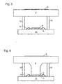
- One of the solutions proposed is for a liquid supply system to provide liquid on only a localized area of the substrate and in between the final element of the projection system and the substrate using a liquid confinement system (the substrate generally has a larger surface area than the final element of the projection system). One way which has been proposed to arrange for this is disclosed in WO 99/49504, hereby incorporated in its entirety by reference. As illustrated in Figures 2 and 3, liquid is supplied by at least one inlet IN onto the substrate, preferably along the direction of movement of the substrate relative to the final element, and is removed by at least one outlet OUT after having passed under the projection system. That is, as the substrate is scanned beneath the element in a -X direction, liquid is supplied at the +X side of the element and taken up at the -X side. Figure 2 shows the arrangement schematically in which liquid is supplied via inlet IN and is taken up on the other side of the element by outlet OUT which is connected to a low pressure source. In the illustration of Figure 2 the liquid is supplied along the direction of movement of the substrate relative to the final element, though this does not need to be the case. Various orientations and numbers of in- and out-lets positioned around the final element are possible, one example is illustrated in Figure 3 in which four sets of an inlet with an outlet on either side are provided in a regular pattern around the final element.
- Another solution which has been proposed is to provide the liquid supply system with a seal member which extends along at least a part of a boundary of the space between the final element of the projection system and the substrate table. Such a solution is illustrated in Figure 4. The seal member is substantially stationary relative to the projection system in the XY plane though there may be some relative movement in the Z direction (in the direction of the optical axis). A seal is formed between the seal member and the surface of the substrate. Preferably the seal is a contactless seal such as a gas seal. Such as system with a gas seal is disclosed in European Patent Application No. 03252955.4 hereby incorporated in its entirety by reference.
- In European Patent Application No. 03257072.3 the idea of a twin or dual stage immersion lithography apparatus is disclosed. Such an apparatus is provided with two stages for supporting the substrate. Leveling measurements are carried out with a stage at a first position, without immersion liquid, and exposure is carried out with a stage at a second position, where immersion liquid is present. Alternatively, the apparatus has only one stage.
- A number of sensors are used at substrate level for evaluating and optimizing imaging performance. These may include transmission image sensors (TIS), spot sensors for measuring exposure radiation dose and integrated lens interferometers at scanner (ILIAS). TIS and ILIAS are described below.
- A TIS is a sensor that is used to measure the position at substrate level of a projected aerial image of a mark pattern at the mask (reticle) level. The projected image at substrate level may be a line pattern with a line width comparable to the wavelength of the exposure radiation. The TIS measures these mask patterns using a transmission pattern with a photocell underneath it. The sensor data may be used to measure the position of the mask with respect to the substrate table in six degrees of freedom (three in translation and three in rotation). In addition, the magnification and scaling of the projected mask may be measured. Since the sensor is preferably capable of measuring the pattern positions and influences of all illumination settings (sigma, lens NA, all masks (binary, PSM, etc.)) a small line width is preferable. The TIS may also be used to measure the optical performance of the tool. Different illumination settings are used in combination with different projected images for measuring properties such as pupil shape, coma, spherical aberration, astigmatism and field curvature.
- An ILIAS is an interferometric wavefront measurement system that may perform static measurements on lens aberrations up to high order. It may be implemented as an integrated measurement system used for system initialization and calibration. Alternatively, it may be used for monitoring and recalibration "on-demand".
- In systems with high NA and in particular in immersion systems, it has been found that conventional sensors at substrate level suffer poor sensitivity.
- It is desirable to provide a sensor at substrate level with high sensitivity and which is suitable for use in a high NA system.
- According to an aspect of the invention, there is provided a lithographic apparatus comprising: an illumination system configured to condition a radiation beam; a support constructed to support a patterning device, the patterning device being capable of imparting the radiation beam with a pattern in its cross-section to form a patterned radiation beam; a substrate table constructed to hold a substrate; a projection system configured to project the patterned radiation beam onto a target portion of the substrate, and a sensor at substrate level comprising a radiation-receiving element, a transmissive plate supporting said radiation-receiving element, and a radiation-detecting means,
wherein said sensor at substrate level is arranged to avoid loss of radiation between said radiation-receiving element and the final element of said radiation-detecting means. - According to a further aspect of the invention, there is provided a device manufacturing method comprising: providing a substrate that is at least partially covered by a layer of radiation-sensitive material; providing a projection beam of radiation using a radiation system; using patterning means to endow the projection beam with a pattern in its cross-section; projecting the patterned beam of radiation onto a target portion of the layer of radiation-sensitive material; providing a sensor at substrate level that receives radiation via a radiation-receiving element and detects said radiation via a radiation-detecting element; and providing means to avoid loss of radiation between said radiation-receiving element and the final element of said radiation-detecting means.
- Embodiments of the invention will now be described, by way of example only, with reference to the accompanying schematic drawings in which corresponding reference symbols indicate corresponding parts, and in which:
- Figure 1 depicts a lithographic apparatus according to an embodiment of the invention;
- Figures 2 and 3 depict a liquid supply system used in a prior art lithographic projection apparatus;
- Figure 4 depicts a liquid supply system according to another prior art lithographic projection apparatus;
- Figure 5 depicts an ILIAS sensor module according to the prior art;
- Figure 6 depicts an ILIAS sensor module with an elongated transmissive plate according to an embodiment of the present invention;
- Figure 7 depicts an ILIAS sensor module with a filler sheet according to an embodiment of the present invention;
- Figure 8a and 8b depict a luminescence based DUV TIS according to the prior art;
- Figure 9 depicts schematically an arrangement of filler sheets in a stack comprising transmissive plate, luminescence layer and photodiode according to the present invention, along with example ray paths;
- Figure 10 depicts schematically two arrangements of a filler sheet sandwiched between a luminescence layer and photodiode according to the present invention, along with example ray paths;
- Figures 11a and 11b depict a non-luminescence based DUV TIS with filler sheets according to the present invention;
- Figure 12 depicts the use of a filler sheet in a stack comprising a transmissive plate and a photodiode, along with example ray paths;
- Figure 13 depicts a sensor at substrate level, comprising a photocell in combination with a luminescence layer, with a filler layer positioned above the luminescence layer;
- Figure 14 depicts a sensor at substrate level, comprising a photocell positioned immediately below the radiation-receiving element;
- Figure 15 depicts a sensor at substrate level, comprising a photocell in combination with a luminescence layer positioned immediately below the radiation-receiving element;
- Figure 16 depicts a sensor at substrate level, comprising a photocell in combination with a luminescence layer positioned immediately below the quartz sensor body;
- Figure 17 depicts a sensor at substrate level, comprising a photocell in combination with a luminescence layer and a diffractive lens; and
- Figure 18 depicts a sensor at substrate level, comprising a photocell in combination with a luminescence layer and a micro-lens.
- In the Figures, corresponding reference symbols indicate corresponding parts.
- Figure 1 schematically depicts a lithographic apparatus according to one embodiment of the invention. The apparatus comprises:
- an illumination system (illuminator) IL configured to condition a radiation beam B (e.g. UV radiation or DUV radiation).
- a support structure (e.g. a mask table) MT constructed to support a patterning device (e.g. a mask) MA and connected to a first positioner PM configured to accurately position the patterning device in accordance with certain parameters;
- a substrate table (e.g. a wafer table) WT constructed to hold a substrate (e.g. a resist-coated wafer) W and connected to a second positioner PW configured to accurately position the substrate in accordance with certain parameters; and
- a projection system (e.g. a refractive projection lens system) PS configured to project a pattern imparted to the radiation beam B by patterning device MA onto a target portion C (e.g. comprising one or more dies) of the substrate W.
- The illumination system may include various types of optical components, such as refractive, reflective, magnetic, electromagnetic, electrostatic or other types of optical components, or any combination thereof, for directing, shaping, or controlling radiation.
- The support structure supports, i.e. bears the weight of, the patterning device. It holds the patterning device in a manner that depends on the orientation of the patterning device, the design of the lithographic apparatus, and other conditions, such as for example whether or not the patterning device is held in a vacuum environment. The support structure can use mechanical, vacuum, electrostatic or other clamping techniques to hold the patterning device. The support structure may be a frame or a table, for example, which may be fixed or movable as required. The support structure may ensure that the patterning device is at a desired position, for example with respect to the projection system. Any use of the terms "reticle" or "mask" herein may be considered synonymous with the more general term "patterning device."
- The term "patterning device" used herein should be broadly interpreted as referring to any device that can be used to impart a radiation beam with a pattern in its cross-section such as to create a pattern in a target portion of the substrate. It should be noted that the pattern imparted to the radiation beam may not exactly correspond to the desired pattern in the target portion of the substrate, for example if the pattern includes phase-shifting features or so called assist features. Generally, the pattern imparted to the radiation beam will correspond to a particular functional layer in a device being created in the target portion, such as an integrated circuit.
- The patterning device may be transmissive or reflective. Examples of patterning devices include masks, programmable mirror arrays, and programmable LCD panels. Masks are well known in lithography, and include mask types such as binary, alternating phase-shift, and attenuated phase-shift, as well as various hybrid mask types. An example of a programmable mirror array employs a matrix arrangement of small mirrors, each of which can be individually tilted so as to reflect an incoming radiation beam in different directions. The tilted mirrors impart a pattern in a radiation beam which is reflected by the mirror matrix.
- The term "projection system" used herein should be broadly interpreted as encompassing any type of projection system, including refractive, reflective, catadioptric, magnetic, electromagnetic and electrostatic optical systems, or any combination thereof, as appropriate for the exposure radiation being used, or for other factors such as the use of an immersion liquid or the use of a vacuum. Any use of the term "projection lens" herein may be considered as synonymous with the more general term "projection system".
- As here depicted, the apparatus is of a transmissive type (e.g. employing a transmissive mask). Alternatively, the apparatus may be of a reflective type (e.g. employing a programmable mirror array of a type as referred to above, or employing a reflective mask).
- The lithographic apparatus may be of a type having two (dual stage) or more substrate tables (and/or two or more mask tables). In such "multiple stage" machines the additional tables may be used in parallel, or preparatory steps may be carried out on one or more tables while one or more other tables are being used for exposure.
- Referring to Figure 1, the illuminator IL receives a radiation beam from a radiation source SO. The source and the lithographic apparatus may be separate entities, for example when the source is an excimer laser. In such cases, the source is not considered to form part of the lithographic apparatus and the radiation beam is passed from the source SO to the illuminator IL with the aid of a beam delivery system BD comprising, for example, suitable directing mirrors and/or a beam expander. In other cases the source may be an integral part of the lithographic apparatus, for example when the source is a mercury lamp. The source SO and the illuminator IL, together with the beam delivery system BD if required, may be referred to as a radiation system.
- The illuminator IL may comprise an adjuster AD for adjusting the angular intensity distribution of the radiation beam. Generally, at least the outer and/or inner radial extent (commonly referred to as σ-outer and σ-inner, respectively) of the intensity distribution in a pupil plane of the illuminator can be adjusted. In addition, the illuminator IL may comprise various other components, such as an integrator IN and a condenser CO. The illuminator may be used to condition the radiation beam, to have a desired uniformity and intensity distribution in its cross-section.
- The radiation beam B is incident on the patterning device (e.g., mask MA), which is held on the support structure (e.g., mask table MT), and is patterned by the patterning device. Having traversed the mask MA, the radiation beam B passes through the projection system PS, which focuses the beam onto a target portion C of the substrate W. With the aid of the second positioner PW and position sensor IF (e.g. an interferometric device, linear encoder or capacitive sensor), the substrate table WT can be moved accurately, e.g. so as to position different target portions C in the path of the radiation beam B. Similarly, the first positioner PM and another position sensor (which is not explicitly depicted in Figure 1) can be used to accurately position the mask MA with respect to the path of the radiation beam B, e.g. after mechanical retrieval from a mask library, or during a scan. In general, movement of the mask table MT may be realized with the aid of a long-stroke module (coarse positioning) and a short-stroke module (fine positioning), which form part of the first positioner PM. Similarly, movement of the substrate table WT may be realized using a long-stroke module and a short-stroke module, which form part of the second positioner PW. In the case of a stepper (as opposed to a scanner) the mask table MT may be connected to a short-stroke actuator only, or may be fixed. Mask MA and substrate W may be aligned using mask alignment marks M1, M2 and substrate alignment marks P1, P2. Although the substrate alignment marks as illustrated occupy dedicated target portions, they may be located in spaces between target portions (these are known as scribe-lane alignment marks). Similarly, in situations in which more than one die is provided on the mask MA, the mask alignment marks may be located between the dies.
- The depicted apparatus could be used in at least one of the following modes:
- 1. In step mode, the mask table MT and the substrate table WT are kept essentially stationary, while an entire pattern imparted to the radiation beam is projected onto a target portion C at one time (i.e. a single static exposure). The substrate table WT is then shifted in the X and/or Y direction so that a different target portion C can be exposed. In step mode, the maximum size of the exposure field limits the size of the target portion C imaged in a single static exposure.
- 2. In scan mode, the mask table MT and the substrate table WT are scanned synchronously while a pattern imparted to the radiation beam is projected onto a target portion C (i.e. a single dynamic exposure). The velocity and direction of the substrate table WT relative to the mask table MT may be determined by the (de-)magnification and image reversal characteristics of the projection system PS. In scan mode, the maximum size of the exposure field limits the width (in the non-scanning direction) of the target portion in a single dynamic exposure, whereas the length of the scanning motion determines the height (in the scanning direction) of the target portion.
- 3. In another mode, the mask table MT is kept essentially stationary holding a programmable patterning device, and the substrate table WT is moved or scanned while a pattern imparted to the radiation beam is projected onto a target portion C. In this mode, generally a pulsed radiation source is employed and the programmable patterning device is updated as required after each movement of the substrate table WT or in between successive radiation pulses during a scan. This mode of operation can be readily applied to maskless lithography that utilizes programmable patterning device, such as a programmable mirror array of a type as referred to above.
-
- Combinations and/or variations on the above described modes of use or entirely different modes of use may also be employed.
- Figures 5 to 18 depict improved substrate-level sensors according to embodiments of the invention. These sensors comprise a radiation-receiving element (2,18) and a radiation-detecting element (8,24,40). Exposure radiation is directed from the final element of the projection system PL through an
immersion liquid 1 at least partly filling a space between the final element of the projection system PL and the substrate W. The detailed configuration of each of these elements depends on the properties of the radiation to be detected. The sensor at substrate level may comprise a photocell only, for use in cases where it is desirable for the photocell to receive the radiation directly. Alternatively, the sensor at substrate level may comprise a luminescence layer in combination with a photocell. In this arrangement, radiation at a first wavelength is absorbed by the luminescence layer and reradiated a short time later at a second (longer) wavelength. This arrangement is useful, for example, where the photocell is designed to work more efficiently at the second wavelength. - The radiation-receiving element (2,18), which may be a layer with a pinhole, a grating or another diffractive element fulfilling a similar function, may be supported on top of a
quartz sensor body 20, i.e. on the same side of the body as the projection system. The radiation-detecting element (8,24,40), in contrast, may be arranged within thesensor body 20, or within a concave region formed on the side of thesensor body 20 facing away from the projection system. - At boundaries between media of different refractive indices a proportion of incident radiation will be reflected and potentially lost from the sensor. For optically smooth surfaces, the extent to which this occurs depends on the angle of incidence of the radiation and the difference in refractive index of the media in question. For radiation incident at and above a "critical angle" (conventionally measured from normal incidence) total internal reflection may occur, leading to serious loss of signal to later elements of the sensor. This may be a particular problem in high NA systems where radiation may have a higher average angle of incidence. The present invention provides arrangements whereby air is excluded from the region between the radiation-receiving (2,18) and radiation-detecting (8,24,40) elements in order to avoid interfaces between media of high refractive index and air.
- In addition to losses due to partial and total internal reflection, absorption may also seriously reduce the intensity of radiation intensity reaching the photocell, as may scattering from interfaces that are not optically smooth.
- A substantial contribution to the reduced sensitivity of the prior art arrangements is loss of radiation from the sensor before it even reaches the final element of the radiation-detecting element. As discussed above, radiation may be lost due to scattering from rough surfaces or via total or partial internal reflection at interfaces within the detector. Alternatively, air gaps containing oxygen and water may lead to substantial absorption of radiation passing through.
- For example, Figure 5 shows an ILIAS sensor module according to the prior art. This module has a shearing
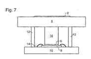
grating structure 2 as radiation-receiving element, supported by atransmissive plate 4, which may be made of glass or quartz. Aquantum conversion layer 6 is positioned immediately above a camera chip 8 (the radiation-detecting element), which is in turn mounted on asubstrate 10. Thesubstrate 10 is connected to thetransmissive plate 4 viaspacers 12 andbonding wires 14 connect the radiation-detecting element to external instrumentation. An air gap is located between thequantum conversion layer 6 and thetransmissive plate 4. In a setup such as this designed for 157 nm radiation, for example, the air gap within the sensor cannot easily be purged so that it will contain significant proportions of oxygen and water, which absorb radiation. Signal is therefore lost and the effect becomes worse for larger angles as these have a longer path length through air. Thus, the dynamic range requirements for the sensor become more severe. - According to an aspect of the invention, the sensor at substrate level may comprise one or more transmissive filler sheets. These sheets may be positioned within the sensor so as to remove air gaps between the radiation-receiving element (2,18) and the final element of the radiation-detecting means (8,24,40). Alternatively or additionally, the transmissive plate may be arranged to extend continuously between the radiation-receiving element (2,18) and the radiation-detecting element (8,24,40), thus avoiding any air gaps in this region. This approach may reduce the need for additional filler sheets and associated interfaces.
- For example, Figures 6 and 7 show improved ILIAS sensor modules according to embodiments of the invention. In Figure 6, the air gap has been removed by changing the shape of the
transmissive plate 4 to fit directly to thecamera 8. This arrangement is made more difficult by the need to provide access for thebonding wires 14 and necessitates an elongated form. From an engineering point of view, the alternative arrangement using transmissive filler sheets shown in Figure 7 is easier to realize. Here, afiller sheet 16 of the same material as thetransmissive plate 4, or of similar optical properties, is inserted between thetransmissive plate 4 and thequantum conversion layer 6. The removal of the air gap reduces transmission losses and relaxes dynamic range requirements (or, alternatively speaking, improves the effective dynamic range). Both arrangements improve refractive index matching and reduce the extent of spurious internal reflections at the interface with thetransmissive plate 4. - The material for each filler sheet may be chosen to be highly transmissive for the predominant wavelength of radiation that will pass through it. Immediately following the radiation-receiving element (2,18) the radiation wavelength may be extremely short (e.g. 157 nm), but luminescence layers (22) occurring later in the sensor may emit longer wavelength radiation in which case it would be advantageous to choose different materials for filler sheets in the respective regions.
- The material for each filler sheet may further be chosen to provide refractive index matching with media with which it is in contact. The refractive index of air is very different from typical sensor components leading to strong partial reflection and a smaller critical angle for total internal reflection. By providing a filler sheet with a refractive index closer to the component in question instead of an air gap, partial reflection is reduced and the critical angle for total internal reflection is increased. This feature has the effect of further improving the effective dynamic range of the sensor.
- The filler sheets may be positioned in contact with optically rough component interfaces and treated so as to follow the contours of the surface roughness. Where sensor elements have been machined they will normally have a surface roughness on the length scale of incident radiation. When a significant refractive index mismatch is present at such a surface, a significant proportion of the incident radiation will inevitably be lost due to scattering at the surface. By using filler sheets and treating them so that they follow the contours of the surface roughness (and thereby purge any air that may exist there) the smaller discontinuity in refractive index reduces the extent of radiation loss at the interface.
- Figure 8a shows a DUV transmission image sensor according to the prior art. Figure 8b shows a magnified view of the processing element for clarity. The pattern of
transmissive grooves 18, constituting the radiation-receiving element in this case, is realized by means of e-beam lithography and dry etching techniques in a thin metal layer deposited on a substrate by means of sputtering. Any DUV light that is projected towards thegrooves 18 is transmitted by the transmissive plate 4 (which may be quartz or fused silica) and hits the underlyingluminescent material 22, or "phosphor". Theluminescent material 22 may consist of a slab of crystalline material that is doped with rare-earth ions, e.g. yttrium-aluminium-gamet doped with cerium (YAG:Ce). The main purpose of theluminescent material 22 is to convert the DUV radiation into more easily detectable visible radiation, which is then detected by thephotodiode 24. DUV radiation that has not been absorbed and converted into visible radiation by thephosphor 22 may be filtered out before it reaches the photodiode 24 (e.g. by a BG-39 or UG filter 26). - In the above arrangement, air may be present in the gaps between components mounted in the
sensor housing 25, yielding a number of air/material/air interfaces that interrupt the propagation of radiation. By considering the path of DUV radiation and radiation arising from luminescence, it is possible to identify regions where radiation is likely to be lost. The first region of interest is the rear-side 28 of thetransmissive plate 4, reached by DUV radiation after it has passed through thegrooves 18 andtransmissive plate 4. Here, the surface has been formed by mechanical means, such as by drilling, and is inevitably rough on the scale of the wavelength of the radiation. Radiation may therefore be lost due to scattering, either back into thetransmissive plate 4 or out past theluminescent material 22. Secondly, after this interface, the DUV light encounters the optically smooth air/YAG:Ce interface, where a substantial amount of reflection may occur due to the refractive index mismatch, particularly in systems of high NA. Thirdly, theluminescent material 22 emits radiation in random directions. Due to its relatively high refractive index, the critical angle for total internal reflection at the YAG:Ce/air boundary is around 33° (there is air in the gap between the YAG:Ce and the filter) from the normal, meaning that a large proportion of radiation incident on the boundary is reflected out of the system and lost through the side walls of theluminescent material 22. Finally, the part of the luminescence that is directed towards the photodiode has to overcome the air/quartz interface on the diode surface where surface roughness may again account for loss of detected signal. - Figures 9 and 10 illustrate schematic arrangements that address the problems of the prior art described above as well as exemplary radiation ray paths.
Filler sheets 30, which may be made from light transmitting plastics, are inserted between components to reduce the effect of radiation scattering at air/material interfaces with high surface roughness or large refractive index discontinuities. For example, thefiller sheets 30 may be arranged to be transmissive for either DUV radiation, visible radiation, or both. Additionally, the refractive index of eachfiller sheet 30 may be tuned to provide the most efficient refractive index matching between media with which it is in contact. Where afiller sheet 30 is in contact with an optically rough surface, some deformation of thefiller sheet 30 may be necessary to ensure that it closely follows the surface roughness and does not leave any tiny air pockets. This may be achieved by mechanically compressing thefiller sheet 30 onto the surface in question. Alternatively, thefiller sheet 30 may be gently heated (avoiding excessive oxidation or other chemical decomposition that may occur at high temperature) until it flows sufficiently to follow the surface roughness. It is also possible to use fluids as filler layers, chosen to have as high a refractive index as possible, for example fomblin. - The filler layer may be arranged to have a refractive index equal to or greater than the refractive index of the immersion liquid. In the typical case where the relevant interfaces (immersion liquid to transmissive plate and transmissive plate to filler sheet) are parallel to each other and perpendicular to the axis of the projection system, this condition ensures that no internal reflection will occur at the transmissive plate to filler sheet interface. If it were required to make these interfaces non-parallel then a corresponding increase in the lower refractive index bound for the
filler sheet 30 may be chosen. - Figure 9 shows a possible implementation of the
filler sheets 30 in a DUV sensor comprising atransmissive plate 4,luminescence layer 22 andphotodiode 38. The right-hand diagram comprisesfiller sheets 30 while, for comparison, the left-hand diagram does not. In each case, arrows show exemplary ray paths through the stack, with internal reflection occurring at the YAG:Ce/diode interface when the filler sheets are absent. - The
filler sheet 30 may either consist of a single sheet, as shown in the left-hand diagram of Figure 10, for example, or of a composite sheet consisting of two layers of different refractive index with amicro-lens array pattern 34 formed at the boundary between the two layers. - According to this embodiment, the filler sheet not only acts to improve refractive index matching and reduce absorption but focuses rays so as to reduce their angle to the normal and thereby improve transmission at later interfaces.
- One or more of the optical components (e.g. transmissive plate, filler sheet and/or luminescence layer) of the sensor at substrate level may comprise an intemal-reflection-enhancing layer on its outer lateral surface. This layer may be constructed by roughening the outer surface and/or applying a metallic layer to it. This feature acts to reflect radiation back into the sensor that would otherwise have been lost.
- The measures discussed above significantly improve the signal-to-noise performance of TIS type sensors, a factor likely to become increasingly critical due to the trend towards designs with ever decreasing line widths of the
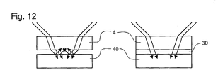
grooves 18 in the radiation-receiving element. In addition to the losses associated with internal sensor interfaces, a large proportion of the signal may also be lost due to inefficient conversion of the DUV radiation to visible radiation within theluminescence layer 22. According to a further embodiment of the invention, theluminescence layer 22 is removed from the sensor and DUV radiation is arranged to impinge directly onto a suitably adaptedphotodiode 40. Photodiodes provide a shorter path from photon to electron (i.e. from radiation to signal) and diodes sensitive to DUV may be obtained with arbitrary shape and size.Such diodes 40 may be capable of detecting DUV radiation down to 50 nm wavelength with a conversion efficiency of the order of 0.20 A/W. Long diode lifetimes are achieved by depositing oxynitride passivation layers on the diode entrance windows. The arrangement is illustrated schematically in Figure 11a. Figure 11b shows a magnified view of the processing element for clarity. Here,photodiodes 40 are positioned below thegrooves 18 in such a way that incident radiation only has to propagate through thegrooves 18, atransmissive plate 4, and a refractive index matching filler sheet 30 (Figure 11b shows two possible variations on the filler sheet, a homogeneous layer (top) and a dual layer with micro-lens patterning (bottom)) in order to reach thephotodiode 40. For the refractive index matching filler sheet 30 a liquid dielectric resist HSQ may be used based on its quartz-like properties after moderate temperature curing. This provides an optimal refractive index match. The diodes may be electronically monitored via the rear connections to facilitate maintenance and eventual replacement. - The path of radiation beams through the above arrangement is illustrated in Figure 12. The right-hand diagram comprises
filler sheets 30 while, for comparison, the left-hand diagram does not. - Figures 13 to 18 depict further embodiments of the invention, wherein light (arrows) propagates from the final element of the projection system PL through the
immersion liquid 1 onto the sensor. In Figures 13 to 16, components are arranged to remove low refractive index parts from the sensor. - In the embodiment according to Figure 13, the sensor comprises a
luminescence layer 22 in combination with aphotocell 24. Afiller sheet 30 is arranged between theluminescence layer 22 and the radiation-receivingelement 2, in such a way as to avoid interfaces with air between those elements. The purpose of the filler layer is to increase the amount of light continuing through the detector. Anair gap 3 is arranged between theluminescence layer 22 and thephotocell 24, which is described below. - In the embodiment according to Figure 14, the sensor comprises a
photocell 40, which is arranged to be in contact with the radiation-receiving element on the opposite side to the projection system. This arrangement avoids all interfaces with air. Absorption may also be reduced because the radiation does not pass through intermediate layers. - In the embodiment according to Figure 15 shows a sensor arrangement analogous to that shown in figure 13. However, an
extended luminescence layer 22 is used to fill the space between the front and rear of thesensor body 20. Interfaces and interface-induced reflections are thereby avoided. Anair gap 3 is arranged between theluminescence layer 22 and thephotocell 24, which is described below. - Figure 16 depicts a further embodiment of the invention, wherein the sensor arrangement comprises a
luminescence layer 22 in combination with aphotocell 24. In this case the luminescence layer may take a flattened form and be located on the side of thesensor body 20 facing away from the projection system and in contact with thesensor body 20, thus avoiding interfaces with air before the luminescence layer. Anair gap 3 is arranged between theluminescence layer 22 and thephotocell 24, which is described below. - Figure 17 depicts an embodiment that comprises a
diffractive lens 30 located between the radiation-receivingelement 2 and the radiation-detectingelement 24. Thediffractive lens 30 acts to focus the incident radiation by diffraction towards theluminescence material 22, thereby improving the ability of the detector to accept rays that are incident at high angles (such as in systems with high NA). The use of a diffraction-based mechanism allows the lens to be constructed in a miniature form. An alternative and/or additional approach is depicted in Figure 18, wherein a micro-lens 40 (operating principally by refraction rather than diffraction) is included in an equivalent position to thediffractive lens 30. In the particular arrangement shown, the micro-lens 40 is formed directly from the material of thesensor body 20. This arrangement avoids having to add the lens as a separate component, which increases system complexity, and also avoids the problem of additional signal loss that may occur due to reflection at interfaces with the lens material. However, a different material may also be used for the micro-lens 40 without departing from the scope of the invention. - In embodiments comprising a
luminescence layer 22 in combination with aphotocell 24, a small air gap (of the order of microns) may be arranged between theluminescence layer 22 and thephotocell 24. The small size of the gap means that even high angle rays that refract to higher angles at the air interface may still impinge on the photocell without making the photocell overly large. In addition, some proportion of radiation arriving at the air interface above the critical angle may still propagate to the photocell via tunneling of the evanescent wave across the air gap. The size of the gap is preferably smaller than the wavelength of incident radiation. - The radiation-receiving element may comprise a grating and or an element having a pinhole, depending on the function of the sensor.
- The sensors may be located at the level of the substrate and in particular such that the radiation-receiving
element 16 is at substantially the same distance from the final element of the projection system as the substrate W. - Although specific reference may be made in this text to the use of lithographic apparatus in the manufacture of ICs, it should be understood that the lithographic apparatus described herein may have other applications, such as the manufacture of integrated optical systems, guidance and detection patterns for magnetic domain memories, flat-panel displays, liquid-crystal displays (LCDs), thin-film magnetic heads, etc. The skilled artisan will appreciate that, in the context of such alternative applications, any use of the terms "wafer" or "die" herein may be considered as synonymous with the more general terms "substrate" or "target portion", respectively. The substrate referred to herein may be processed, before or after exposure, in for example a track (a tool that typically applies a layer of resist to a substrate and develops the exposed resist), a metrology tool and/or an inspection tool. Where applicable, the disclosure herein may be applied to such and other substrate processing tools. Further, the substrate may be processed more than once, for example in order to create a multi-layer IC, so that the term substrate used herein may also refer to a substrate that already contains multiple processed layers.
- The terms "radiation" and "beam" used herein encompass all types of electromagnetic radiation, including ultraviolet (UV) radiation (e.g. having a wavelength of or about 365, 248, 193, 157 or 126 nm).
- The term "lens", where the context allows, may refer to any one or combination of various types of optical components, including refractive and reflective optical components.
- While specific embodiments of the invention have been described above, it will be appreciated that the invention may be practiced otherwise than as described. For example, the invention may take the form of a computer program containing one or more sequences of machine-readable instructions describing a method as disclosed above, or a data storage medium (e.g. semiconductor memory, magnetic or optical disk) having such a computer program stored therein.
- The present invention can be applied to any immersion lithography apparatus, in particular, but not exclusively, those types mentioned above.
- The descriptions above are intended to be illustrative, not limiting. Thus, it will be apparent to one skilled in the art that modifications may be made to the invention as described without departing from the scope of the claims set out below.
Claims (19)
- A lithographic apparatus comprising: an illumination system configured to condition a radiation beam; a support constructed to support a patterning device, the patterning device being capable of imparting the radiation beam with a pattern in its cross-section to form a patterned radiation beam; a substrate table constructed to hold a substrate; a projection system configured to project the patterned radiation beam onto a target portion of the substrate, and a sensor at substrate level comprising a radiation-receiving element, a transmissive plate supporting said radiation-receiving element, and a radiation-detecting means,
characterized in that said sensor at substrate level is arranged to avoid loss of radiation between said radiation-receiving element and the final element of said radiation-detecting means. - A lithographic apparatus according to claim 1, wherein said sensor at substrate level comprises one or more transmissive filler sheet(s).
- A lithographic apparatus according to claim 2, wherein said filler sheet(s) is (are) arranged to avoid air gaps between said radiation-receiving element and the final element of said radiation-detecting means.
- A lithographic apparatus according to claim 2 or 3, wherein each said filler sheet is arranged to be transmissive for the predominant wavelength of radiation passing through it.
- A lithographic apparatus according to any one of claims 2 to 4, wherein each said filler sheet is arranged to maximize refractive index matching with surrounding media.
- A lithographic apparatus according to any one of claims 2 to 5, wherein the filler sheets are positioned in contact with optically rough component interfaces and treated so as to follow the contours of the surface roughness.
- A lithographic apparatus according to claim 6, wherein said treatment of said filler sheets comprises deformation by mechanical compression or heating.
- A lithographic apparatus according to claim 1, wherein said transmissive plate is arranged to extend continuously between said radiation-receiving element and said radiation-detecting element.
- A lithographic apparatus according to any one of the preceding claims, wherein one or more of the optical components of said sensor at substrate level comprise(s) an internal-reflection-enhancing layer on its (their) outer lateral surface(s).
- A lithographic apparatus according to claim 9, wherein said internal-reflection-enhancing layer comprises a roughened depth of said outer lateral surface in combination with a metal coating.
- A lithographic apparatus according to any one of claims 2 to 10, wherein said filler layer has a refractive index equal to or greater than the refractive index of an immersion liquid at least partly filling a space between a final element of said projection system and said substrate.
- A lithographic apparatus according to any one of the preceding claims, wherein said radiation-detecting element comprises a photocell or a photocell in combination with a luminescence layer.
- A lithographic apparatus according to any one of claims 1 to 11, wherein said radiation-detecting element comprises a photocell adapted to detect DUV radiation directly.
- A lithographic apparatus according to claim 1 or 2, wherein air gaps between said radiation-receiving element and said final component of the radiation-detecting element are of a thickness less than the predominant wavelength of radiation expected to pass through each said air gap.
- A lithographic apparatus according to any one of the preceding claims, wherein said radiation-receiving element is a grating or an element having a pinhole.
- A lithographic apparatus according to any one of the preceding claims, wherein said filler sheet comprises two layers of different refractive indices, a micro-lens array being formed at the interface between said two layers.
- A lithographic apparatus according to any one of the preceding claims, further comprising a diffractive lens located between said radiation receiving element and said radiation-detecting element.
- A lithographic apparatus according to any one of the preceding claims, further comprising a micro-lens located between said radiation-receiving element and said radiation-detecting element.
- A device manufacturing method comprising the steps of: providing a substrate that is at least partially covered by a layer of radiation-sensitive material; providing a projection beam of radiation using a radiation system; using patterning means to endow the projection beam with a pattern in its cross-section; projecting the patterned beam of radiation onto a target portion of the layer of radiation-sensitive material; and providing a sensor at substrate level that receives radiation via a radiation-receiving element and detects said radiation via a radiation-detecting element,
characterized by the step of providing means to avoid loss of radiation between said radiation-receiving element and the final element of said radiation-detecting means.
Priority Applications (1)
| Application Number | Priority Date | Filing Date | Title |
|---|---|---|---|
| EP04254910A EP1510870A1 (en) | 2003-08-29 | 2004-08-16 | Lithographic apparatus and device manufacturing method |
Applications Claiming Priority (3)
| Application Number | Priority Date | Filing Date | Title |
|---|---|---|---|
| EP03255395 | 2003-08-29 | ||
| EP03255395 | 2003-08-29 | ||
| EP04254910A EP1510870A1 (en) | 2003-08-29 | 2004-08-16 | Lithographic apparatus and device manufacturing method |
Publications (1)
| Publication Number | Publication Date |
|---|---|
| EP1510870A1 true EP1510870A1 (en) | 2005-03-02 |
Family
ID=34105758
Family Applications (1)
| Application Number | Title | Priority Date | Filing Date |
|---|---|---|---|
| EP04254910A Withdrawn EP1510870A1 (en) | 2003-08-29 | 2004-08-16 | Lithographic apparatus and device manufacturing method |
Country Status (1)
| Country | Link |
|---|---|
| EP (1) | EP1510870A1 (en) |
Cited By (14)
| Publication number | Priority date | Publication date | Assignee | Title |
|---|---|---|---|---|
| EP1670043A2 (en) * | 2003-09-29 | 2006-06-14 | Nikon Corporation | Exposure apparatus, exposure method, and device manufacturing method |
| EP1696272A3 (en) * | 2005-02-28 | 2006-09-27 | ASML Netherlands BV | A sensor for use in a lithographic apparatus |
| US7230676B1 (en) | 2006-03-13 | 2007-06-12 | Asml Netherlands B.V. | Lithographic apparatus and device manufacturing method |
| EP1868034A1 (en) * | 2006-06-15 | 2007-12-19 | ASML Netherlands BV | Wave front sensor with grey filter and lithographic apparatus comprising same |
| US7459669B2 (en) | 2005-12-30 | 2008-12-02 | Asml Netherlands B.V. | Sensor and lithographic apparatus |
| US7483120B2 (en) | 2006-05-09 | 2009-01-27 | Asml Netherlands B.V. | Displacement measurement system, lithographic apparatus, displacement measurement method and device manufacturing method |
| US7515281B2 (en) | 2005-04-08 | 2009-04-07 | Asml Netherlands B.V. | Lithographic apparatus and device manufacturing method |
| DE102008041436A1 (en) | 2007-10-02 | 2009-04-09 | Carl Zeiss Smt Ag | Optical membrane element |
| US7675605B2 (en) | 2007-06-29 | 2010-03-09 | Asml Netherlands B.V. | Device and method for transmission image sensing |
| US7768625B2 (en) | 2005-06-02 | 2010-08-03 | Canon Kabushiki Kaisha | Photo detector unit and exposure apparatus having the same |
| US8120763B2 (en) | 2002-12-20 | 2012-02-21 | Carl Zeiss Smt Gmbh | Device and method for the optical measurement of an optical system by using an immersion fluid |
| US9429495B2 (en) | 2004-06-04 | 2016-08-30 | Carl Zeiss Smt Gmbh | System for measuring the image quality of an optical imaging system |
| US20170343905A1 (en) * | 2006-02-21 | 2017-11-30 | Nikon Corporation | Pattern forming apparatus, mark detecting apparatus, exposure apparatus, pattern forming method, exposure method, and device manufacturing method |
| USRE47943E1 (en) | 2005-04-08 | 2020-04-14 | Asml Netherlands B.V. | Dual stage lithographic apparatus and device manufacturing method |
Citations (5)
| Publication number | Priority date | Publication date | Assignee | Title |
|---|---|---|---|---|
| US4540277A (en) * | 1982-07-09 | 1985-09-10 | Perkin-Elmer Censor Anstalt | Device for the projection printing of masks into a workpiece |
| EP0445871A1 (en) * | 1990-03-05 | 1991-09-11 | ASM Lithography B.V. | Apparatus for and method of projecting a mask pattern on a substrate |
| JPH10340846A (en) * | 1997-06-10 | 1998-12-22 | Nikon Corp | Aligner, its manufacture, exposing method and device manufacturing method |
| EP1182511A1 (en) * | 2000-08-25 | 2002-02-27 | Asm Lithography B.V. | Lithographic apparatus |
| EP1184727A1 (en) * | 2000-09-01 | 2002-03-06 | Asm Lithography B.V. | Lithographic apparatus |
-
2004
- 2004-08-16 EP EP04254910A patent/EP1510870A1/en not_active Withdrawn
Patent Citations (5)
| Publication number | Priority date | Publication date | Assignee | Title |
|---|---|---|---|---|
| US4540277A (en) * | 1982-07-09 | 1985-09-10 | Perkin-Elmer Censor Anstalt | Device for the projection printing of masks into a workpiece |
| EP0445871A1 (en) * | 1990-03-05 | 1991-09-11 | ASM Lithography B.V. | Apparatus for and method of projecting a mask pattern on a substrate |
| JPH10340846A (en) * | 1997-06-10 | 1998-12-22 | Nikon Corp | Aligner, its manufacture, exposing method and device manufacturing method |
| EP1182511A1 (en) * | 2000-08-25 | 2002-02-27 | Asm Lithography B.V. | Lithographic apparatus |
| EP1184727A1 (en) * | 2000-09-01 | 2002-03-06 | Asm Lithography B.V. | Lithographic apparatus |
Non-Patent Citations (2)
| Title |
|---|
| PATENT ABSTRACTS OF JAPAN vol. 1999, no. 03 31 March 1999 (1999-03-31) * |
| PELLICORI S F: "OPTICAL BONDING AGENTS FOR IR AND UV REFRACTING ELEMENTS", PROCEEDINGS OF SPIE, SPIE, US, vol. 1535, 1 May 1991 (1991-05-01), pages 48 - 54, XP001122190, ISSN: 0277-786X, DOI: 10.1117/12.48302 * |
Cited By (30)
| Publication number | Priority date | Publication date | Assignee | Title |
|---|---|---|---|---|
| US8836929B2 (en) | 2002-12-20 | 2014-09-16 | Carl Zeiss Smt Gmbh | Device and method for the optical measurement of an optical system by using an immersion fluid |
| US8120763B2 (en) | 2002-12-20 | 2012-02-21 | Carl Zeiss Smt Gmbh | Device and method for the optical measurement of an optical system by using an immersion fluid |
| US8305552B2 (en) | 2003-09-29 | 2012-11-06 | Nikon Corporation | Exposure apparatus, exposure method, and method for producing device |
| US8139198B2 (en) | 2003-09-29 | 2012-03-20 | Nikon Corporation | Exposure apparatus, exposure method, and method for producing device |
| US10025194B2 (en) | 2003-09-29 | 2018-07-17 | Nikon Corporation | Exposure apparatus, exposure method, and method for producing device |
| US9513558B2 (en) | 2003-09-29 | 2016-12-06 | Nikon Corporation | Exposure apparatus, exposure method, and method for producing device |
| EP1670043A4 (en) * | 2003-09-29 | 2008-07-30 | Nikon Corp | Exposure apparatus, exposure method, and device manufacturing method |
| EP1670043A2 (en) * | 2003-09-29 | 2006-06-14 | Nikon Corporation | Exposure apparatus, exposure method, and device manufacturing method |
| US8039807B2 (en) | 2003-09-29 | 2011-10-18 | Nikon Corporation | Exposure apparatus, exposure method, and method for producing device |
| US8749759B2 (en) | 2003-09-29 | 2014-06-10 | Nikon Corporation | Exposure apparatus, exposure method, and method for producing device |
| US9429495B2 (en) | 2004-06-04 | 2016-08-30 | Carl Zeiss Smt Gmbh | System for measuring the image quality of an optical imaging system |
| US8629418B2 (en) | 2005-02-28 | 2014-01-14 | Asml Netherlands B.V. | Lithographic apparatus and sensor therefor |
| US7282701B2 (en) | 2005-02-28 | 2007-10-16 | Asml Netherlands B.V. | Sensor for use in a lithographic apparatus |
| EP1696272A3 (en) * | 2005-02-28 | 2006-09-27 | ASML Netherlands BV | A sensor for use in a lithographic apparatus |
| US7515281B2 (en) | 2005-04-08 | 2009-04-07 | Asml Netherlands B.V. | Lithographic apparatus and device manufacturing method |
| USRE47943E1 (en) | 2005-04-08 | 2020-04-14 | Asml Netherlands B.V. | Dual stage lithographic apparatus and device manufacturing method |
| US7768625B2 (en) | 2005-06-02 | 2010-08-03 | Canon Kabushiki Kaisha | Photo detector unit and exposure apparatus having the same |
| US7459669B2 (en) | 2005-12-30 | 2008-12-02 | Asml Netherlands B.V. | Sensor and lithographic apparatus |
| US20170343905A1 (en) * | 2006-02-21 | 2017-11-30 | Nikon Corporation | Pattern forming apparatus, mark detecting apparatus, exposure apparatus, pattern forming method, exposure method, and device manufacturing method |
| US10234773B2 (en) * | 2006-02-21 | 2019-03-19 | Nikon Corporation | Pattern forming apparatus, mark detecting apparatus, exposure apparatus, pattern forming method, exposure method, and device manufacturing method |
| US10409173B2 (en) | 2006-02-21 | 2019-09-10 | Nikon Corporation | Pattern forming apparatus, mark detecting apparatus, exposure apparatus, pattern forming method, exposure method, and device manufacturing method |
| US7230676B1 (en) | 2006-03-13 | 2007-06-12 | Asml Netherlands B.V. | Lithographic apparatus and device manufacturing method |
| US7483120B2 (en) | 2006-05-09 | 2009-01-27 | Asml Netherlands B.V. | Displacement measurement system, lithographic apparatus, displacement measurement method and device manufacturing method |
| US7388652B2 (en) | 2006-06-15 | 2008-06-17 | Asml Netherlands B.V. | Wave front sensor with grey filter and lithographic apparatus comprising same |
| EP1868034A1 (en) * | 2006-06-15 | 2007-12-19 | ASML Netherlands BV | Wave front sensor with grey filter and lithographic apparatus comprising same |
| US7675605B2 (en) | 2007-06-29 | 2010-03-09 | Asml Netherlands B.V. | Device and method for transmission image sensing |
| US9036130B2 (en) | 2007-06-29 | 2015-05-19 | Asml Netherlands B.V. | Device and method for transmission image sensing |
| DE102008041436A1 (en) | 2007-10-02 | 2009-04-09 | Carl Zeiss Smt Ag | Optical membrane element |
| US9075321B2 (en) | 2007-10-02 | 2015-07-07 | Carl Zeiss Smt Gmbh | Optical membrane element having a longitudinally adjustable connecting element |
| US10254655B2 (en) | 2007-10-02 | 2019-04-09 | Carl Zeiss Smt Gmbh | Optical membrane element having a longitudinally adjustable connecting element |
Similar Documents
| Publication | Publication Date | Title |
|---|---|---|
| US11003096B2 (en) | Lithographic apparatus and device manufacturing method | |
| EP1696272B1 (en) | A sensor for use in a lithographic apparatus | |
| US7589818B2 (en) | Lithographic apparatus, alignment apparatus, device manufacturing method, and a method of converting an apparatus | |
| US20090115987A1 (en) | Position measurement system and lithographic apparatus | |
| EP1510870A1 (en) | Lithographic apparatus and device manufacturing method | |
| EP1447718A2 (en) | Exposure apparatus and method | |
| TWI448822B (en) | Lithographic apparatus, radiation sensor and method of manufacturing a radiation sensor | |
| JP4532927B2 (en) | Exposure equipment | |
| US7459669B2 (en) | Sensor and lithographic apparatus | |
| US7715000B2 (en) | Particle detection system, and lithographic apparatus provided with such particle detection system | |
| WO2021028295A1 (en) | Lithographic apparatus and ultraviolet radiation control system |
Legal Events
| Date | Code | Title | Description |
|---|---|---|---|
| PUAI | Public reference made under article 153(3) epc to a published international application that has entered the european phase |
Free format text: ORIGINAL CODE: 0009012 |
|
| AK | Designated contracting states |
Kind code of ref document: A1 Designated state(s): AT BE BG CH CY CZ DE DK EE ES FI FR GB GR HU IE IT LI LU MC NL PL PT RO SE SI SK TR |
|
| AX | Request for extension of the european patent |
Extension state: AL HR LT LV MK |
|
| 17P | Request for examination filed |
Effective date: 20050426 |
|
| AKX | Designation fees paid |
Designated state(s): DE FR GB IT NL |
|
| STAA | Information on the status of an ep patent application or granted ep patent |
Free format text: STATUS: THE APPLICATION IS DEEMED TO BE WITHDRAWN |
|
| 18D | Application deemed to be withdrawn |
Effective date: 20130221 |