EP1510806A1 - Three-dimensional structural body composed of silicon fine wire, its manufacturing method, and device using same - Google Patents
Three-dimensional structural body composed of silicon fine wire, its manufacturing method, and device using same Download PDFInfo
- Publication number
- EP1510806A1 EP1510806A1 EP03730767A EP03730767A EP1510806A1 EP 1510806 A1 EP1510806 A1 EP 1510806A1 EP 03730767 A EP03730767 A EP 03730767A EP 03730767 A EP03730767 A EP 03730767A EP 1510806 A1 EP1510806 A1 EP 1510806A1
- Authority
- EP
- European Patent Office
- Prior art keywords
- fine wires
- dimensional structure
- silicon
- silicon fine
- producing
- Prior art date
- Legal status (The legal status is an assumption and is not a legal conclusion. Google has not performed a legal analysis and makes no representation as to the accuracy of the status listed.)
- Withdrawn
Links
Images










Classifications
-
- G—PHYSICS
- G01—MEASURING; TESTING
- G01Q—SCANNING-PROBE TECHNIQUES OR APPARATUS; APPLICATIONS OF SCANNING-PROBE TECHNIQUES, e.g. SCANNING PROBE MICROSCOPY [SPM]
- G01Q70/00—General aspects of SPM probes, their manufacture or their related instrumentation, insofar as they are not specially adapted to a single SPM technique covered by group G01Q60/00
- G01Q70/16—Probe manufacture
-
- G—PHYSICS
- G01—MEASURING; TESTING
- G01Q—SCANNING-PROBE TECHNIQUES OR APPARATUS; APPLICATIONS OF SCANNING-PROBE TECHNIQUES, e.g. SCANNING PROBE MICROSCOPY [SPM]
- G01Q70/00—General aspects of SPM probes, their manufacture or their related instrumentation, insofar as they are not specially adapted to a single SPM technique covered by group G01Q60/00
- G01Q70/06—Probe tip arrays
-
- G—PHYSICS
- G01—MEASURING; TESTING
- G01Q—SCANNING-PROBE TECHNIQUES OR APPARATUS; APPLICATIONS OF SCANNING-PROBE TECHNIQUES, e.g. SCANNING PROBE MICROSCOPY [SPM]
- G01Q60/00—Particular types of SPM [Scanning Probe Microscopy] or microscopes; Essential components thereof
- G01Q60/24—AFM [Atomic Force Microscopy] or apparatus therefor, e.g. AFM probes
- G01Q60/38—Probes, their manufacture, or their related instrumentation, e.g. holders
-
- B—PERFORMING OPERATIONS; TRANSPORTING
- B82—NANOTECHNOLOGY
- B82Y—SPECIFIC USES OR APPLICATIONS OF NANOSTRUCTURES; MEASUREMENT OR ANALYSIS OF NANOSTRUCTURES; MANUFACTURE OR TREATMENT OF NANOSTRUCTURES
- B82Y35/00—Methods or apparatus for measurement or analysis of nanostructures
-
- Y—GENERAL TAGGING OF NEW TECHNOLOGICAL DEVELOPMENTS; GENERAL TAGGING OF CROSS-SECTIONAL TECHNOLOGIES SPANNING OVER SEVERAL SECTIONS OF THE IPC; TECHNICAL SUBJECTS COVERED BY FORMER USPC CROSS-REFERENCE ART COLLECTIONS [XRACs] AND DIGESTS
- Y10—TECHNICAL SUBJECTS COVERED BY FORMER USPC
- Y10S—TECHNICAL SUBJECTS COVERED BY FORMER USPC CROSS-REFERENCE ART COLLECTIONS [XRACs] AND DIGESTS
- Y10S438/00—Semiconductor device manufacturing: process
- Y10S438/942—Masking
- Y10S438/947—Subphotolithographic processing
Definitions
- the present invention relates to a three-dimensional structure composed of silicon fine wires.
- the present invention relates to a three-dimensional structure using wires on the order of nanometers (referred to as nano) to micrometers formed by etching utilizing the crystallinity of silicon etc. as elements, a method for producing the same, and a device including the same.
- a plate or block structure composed of silicon or a structure formed by bending a metal conducting wire provides elements such as oscillators and coils.
- a tip magnetized with cobalt or iron etc. is used as a tip of an atomic force microscope to detect a magnetic field.
- a plate-shaped cantilever used in a known scanning force microscope within a scanning electron microscope causes the following problems: When scanning electron microscopy observation is performed perpendicularly to the sample, the cantilever blocks the observation point, so that it is difficult to observe the sample, and to identify the observation point.
- the present invention provides the following:
- the present invention provides the following features:
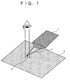
- Fig. 1 is a schematic view of a device having a tip supported by a plurality of fine wires according to an embodiment of the present invention.
- reference numeral 1 indicates a cantilever base
- reference numeral 2 indicates a plurality of fine wires
- reference numeral 3 indicates a tip
- reference numeral 4 indicates a sample.
- the tip 3 is supported by a plurality of fine wires [on the order of nanometers (hereinafter abbreviated as nano) to micrometers], the observation portion of the sample 4 is not blocked. As a result, the portion being observed with the tip 3 can be readily observed with an optical microscope or a scanning microscope.
- the present inventors have already proposed a fine mechanical oscillator formed using a semiconductor material, a method for producing the same, and a measuring device including the same in the above-cited Patent Document 1.
- Fig. 2 is a perspective view of an oscillator (device) having a tip supported by a plurality of fine wires according to an embodiment of the present invention.
- reference numeral 100 indicates an oscillator base
- reference numerals 101 and 102 indicate two fine wires
- reference numeral 103 indicates a tip formed at the intersection of the two fine wires 101 and 102.
- Fig. 3 is a perspective view of a fine coil (device) composed of a plurality of fine wires according to an embodiment of the present invention.
- reference numeral 200 indicates a fine coil base
- reference numeral 201 indicates a fine coil composed of V-shaped fine wires.
- Fig. 4 is a perspective view of an oscillator (device) having tips supported by two doubly-supported fine wires according to an embodiment of the present invention.
- reference numeral 300 indicates oscillator bases disposed at both sides
- reference numerals 301 and 302 indicate two fine wires extending from the oscillator bases 300 disposed at both sides thereof, respectively
- reference numeral 303 indicates tips formed at the intersection of the two fine wires 301 and 302.
- double coils composed of the two doubly-supported fine wires may be formed without forming the tips 303 shown in Fig. 4.
- Fig. 5 is a perspective view of a fine coil (device) having a grid structure composed of fine wires according to an embodiment of the present invention.
- reference numeral 400 indicates a fine coil base
- reference numeral 401 indicates a fine coil having a grid structure composed of fine wires. This device can also be formed in three-dimensional structure.
- Fig. 6 is a perspective view of an oscillator (device) having a tip supported by a plurality of fine wires and used to detect the temperature-dependent resistance variation.
- Fig. 7 is a drawing showing a resistance bridge thereof.
- reference numeral 500 indicates a cantilever support
- reference numeral 501 indicates a plurality of fine wires
- reference numeral 502 indicates a tip.
- each of the cantilevers composed of the fine wires 501 is doped with boron to provide electrical conductivity.
- the resistance bridge shown in Fig. 7 is formed at the cantilever support 500. As a result, the resistance variation due to the temperature of the cantilever can be detected. Because of the significantly low heat capacity, this device can provide high sensitivity and response frequency.
- symbol r 1 represents the resistance of a plurality of the fine wire portions
- symbol r 2 and symbol r 3 represent the resistances of the cantilever support 500.
- single-crystal silicon is etched with potassium hydroxide (KOH) to provide a fine wire composed of a plurality of crystal faces.
- KOH potassium hydroxide
- An example of such a fine wire is composed of two silicon ⁇ 111 ⁇ surfaces and a silicon ⁇ 100 ⁇ surface.
- Silicon single-crystals have the ⁇ 111 ⁇ surface and its equivalent surfaces disposed in two or more directions. Therefore, depending on the combination of the crystal faces, a fine wire having different axial directions can be produced by etching the single-crystal silicon.
- a one-dimensional line and various two or three-dimensional structures such as a coil structure, a grid structure, a network structure, and an oscillator structure, can be achieved.
- Such a three-dimensional structure is produced using a multilayered structure composed of, for example, silicon and silicon oxide by masking appropriate areas according to whether the areas are to be etched or not.
- the structures produced by the present invention can be used as a beam, a V-shaped coil, a V-shaped resistor, a grid structure, and a three-dimensionally linked structure. In any case, in known methods, these structures are made by hand or by combining plate-shaped components. In contrast, the present invention provides the following advantages: The structure can be miniaturized, a plurality of the structures can be produced at the same time, the structure can be produced with high uniformity, the structure can be produced three-dimensionally, the frequency of the structure can be increased, and oscillation loss of the structure can be decreased.
- the above beam can be used as a stylus, a singly-supported beam, or a probe.
- the V-shaped coil can be used as a fine coil.
- the V-shaped resistor can be used as a probe for temperature mapping in a minute area by utilizing the temperature-dependent resistance variation.
- the grid structure can be used as a physical filter or a physical and chemical filter by modifying the surface thereof.
- the grid structure which is a kind of sponge structure, can achieve a predetermined elasticity, and functions as a filter that selects light depending on the direction or the wavelength.
- the structure when the structure is vibrated, the structure functions as an optical modulation element.
- the absorption of a specific substance can be detected as a change in vibration characteristics of the structure by combining the filter function of the specific substance with the oscillator function.
- the inside of the fine wires is used as a waveguide for light or a waveguide for oscillation, thereby controlling the propagation of the light or the oscillation.
- fine wires on the order of nano to micrometers can be achieved by wet etching utilizing the crystallinity of silicon etc., and a three-dimensional structure using the fine wires as elements can be achieved.
- This technology allows elements such as an oscillator, a net, a coil, a heat-generating loop, a filter, and a magnetic sensor on the order of microns to submicrons to be produced.
- the oscillator can detect force or mass
- the net can trap a sample having a specific particle size
- the coil can generate a fine magnetic field or can detect such a magnetic field
- the heat-generating loop can measure the temperature distribution of a sample.
- This method is applicable to mass production of a three-dimensional structure composed of millions to hundreds of millions of fine wires.
- Fig. 8 is a schematic view of a fine coil (device) to which a modulation function can be added, according to an embodiment of the present invention.
- reference numeral 600 indicates a fine coil support
- reference numeral 601 indicates a fine coil composed of fine wires
- reference numeral 602 indicates a sample.
- the fine coil 601 when current flows in the fine coil 601 composed of fine wires, the fine coil 601 can detect the Lorentz force or its gradient due to the magnetic field of the sample 602 as a force applied in the oscillation direction.
- This device allows a magnetic profile to be measured without using the characteristics of a magnetic tip. Furthermore, a modulation function such as modulation of the current, which cannot be added to known magnetic tips, can be added to this device.
- the present invention is applicable to a scanning probe microscope, oscillation measurement, analysis of characteristics of surfaces and interfaces, an electric circuit, a mass detector, an electrical circuit network, a substance-trapping filter, and an elastic material.
- the present invention is also applicable to the measurements of temperature, the temperature distribution of electronic devices, and the temperature distribution and metabolism of biological materials.
- a cantilever generally represents a cantilever used in an atomic force microscope
- the wording "a probe” represents a probe which is not limited to the cantilever used in the atomic force microscope, but represents an element used for various applications such as mass detection and magnetic field detection.
- Fig. 9 shows cantilevers functioning as probes composed of silicon fine wires according to an embodiment of the present invention.
- Fig. 9(a) is a perspective view thereof
- Fig. 9(b) is a plan view thereof
- Fig. 9(c) is a cross-sectional view taken along line L-L in Fig. 9(b).
- reference numeral 701 indicates a handling wafer
- reference numeral 702 indicates a buried oxide film
- reference numeral 703 indicates a silicon-on-insulator (SOI) layer
- reference numeral 707 indicates silicon fine wires (cantilevers composed of singly-supported beams), which are formed by utilizing the crystallinity of the SOI layer 703.
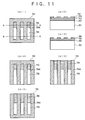
- the method for producing a three-dimensional structure composed of silicon fine wires includes the steps of preparing an SOI substrate having a surface composed of the ⁇ 100 ⁇ surface of silicon single-crystals thereon; forming a silicon oxide film 704 on a part of an SOI layer 703 of the SOI substrate; forming a silicon nitride film 705 on the SOI layer 703 and the silicon oxide film 704; removing a part of the silicon nitride film 705 to expose the SOI layer 703 such that elongated shapes are repeatedly arranged side-by-side so as to be parallel to the ⁇ 110> direction; removing the exposed SOI layer 703 by wet etching with an alkaline solution; thermally oxidizing the ⁇ 111 ⁇ surfaces 703A exposed by the wet etching to form a thermally-oxidized film 706; removing a part of the remaining silicon nitride film 705; wet etching the newly exposed SOI layer 703 with an alkaline solution;
- Fig. 15 shows cantilevers functioning as probes composed of silicon fine wires according to a first modification of the embodiment of the present invention.
- Fig. 15(a) is a perspective view thereof
- Fig. 15(b) is a plan view thereof
- Fig. 15(c) is a cross-sectional view taken along line M-M in Fig. 15(b).
- proximal ends of the silicon fine wires [cantilevers (singly-supported beams composed of fine wires)] 708 are aligned.
- the silicon fine wires 708 are formed such that the length of each fine wire gradually changes from one to the next.
- Other structures are the same as those of the above silicon fine wires.
- Fig. 16 shows cantilevers functioning as probes composed of silicon fine wires according to a second modification of the embodiment of the present invention.
- Fig. 16(a) is a perspective view thereof
- Fig. 16(b) is a plan view thereof
- Fig. 16(c) is a cross-sectional view taken along line N-N in Fig. 16(b).
- distal ends of silicon fine wires [cantilevers (singly-supported beams composed of fine wires)] 709 are formed on the same line, whereas the proximal ends of the silicon fine wires form a slanted shape. As a result, the length of each fine wire gradually changes from one to the next.
- Other structures are the same as those of the above silicon fine wires.
- singly-supported beams composed of silicon fine wires that suffer no damage such as crystal defects can be formed by utilizing the crystallinity of silicon, in contrast to a known example in which cantilevers are formed by anisotropic etching (such as RIE) regardless of the crystallinity of silicon.
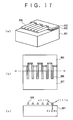
- Fig. 17 shows cantilevers functioning as probes composed of silicon fine wires according to an embodiment of the present invention.
- Fig. 17(a) is a perspective view thereof
- Fig. 17(b) is a plan view thereof
- Fig. 17(c) is a cross-sectional view taken along line H-H in Fig. 17(b).
- reference numeral 801 indicates a handling wafer
- reference numeral 802 indicates a buried oxide film
- reference numeral 803 indicates an SOI layer
- reference numeral 806 indicates silicon fine wires (cantilevers composed of singly-supported beams), which are formed by utilizing the crystallinity of the SOI layer 803.
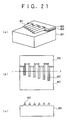
- Fig. 21 shows cantilevers functioning as probes composed of silicon fine wires according to a modification of the embodiment of the present invention.
- Fig. 21(a) is a perspective view thereof
- Fig. 21(b) is a plan view thereof
- Fig. 21(c) is a cross-sectional view taken along line I-I in Fig. 21(b).
- proximal ends of silicon fine wires [cantilevers (singly-supported beams composed of fine wires)] 807 have different shapes on the two lateral sides of each fine wire. Furthermore, the silicon fine wires [cantilevers (singly-supported beams composed of fine wires)] 807 are formed such that the length of each fine wire gradually changes from one to the next. Other structures are the same as those of the above silicon fine wires.
- the singly-supported beams 806 and 807 in which the proximal ends of the fine wires functioning as probes have different shapes on the two lateral sides of each fine wire can be produced inexpensively by a simple process that omits a step of forming a silicon oxide film.
- These singly-supported beams have a durable structure because the proximal ends of the singly-supported beams have an asymmetrical shape. Accordingly, singly-supported beams having durability against aging, not being easily broken, and utilizing the crystallinity of silicon can be formed.
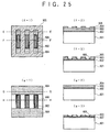
- Fig. 22 shows doubly-supported beams functioning as probes composed of silicon fine wires according to an embodiment of the present invention.
- Fig. 22(a) is a perspective view thereof
- Fig. 22(b) is a plan view thereof
- Fig. 22(c) is a cross-sectional view taken along line K-K in Fig. 22(b).
- reference numeral 901 indicates a handling wafer
- reference numeral 902 indicates a buried oxide film
- reference numeral 903 indicates an SOI layer
- reference numeral 907 indicates silicon fine wires (doubly-supported beams), which are formed by utilizing the crystallinity of the SOI layer 903.
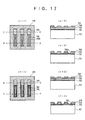
- the method for producing a three-dimensional structure composed of silicon fine wires includes the steps of preparing an SOI substrate having a surface composed of the ⁇ 100 ⁇ surface of silicon single-crystals thereon; forming a silicon oxide film 904 on both ends of an SOI layer 903 of the SOI substrate; forming a silicon nitride film 905 on the silicon oxide film 904; removing a part of the silicon nitride film 905 to expose the SOI layer 903 such that elongated shapes are repeatedly arranged side-by-side so as to be parallel to the ⁇ 110> direction; removing the exposed SOI layer 903 by wet etching with an alkaline solution; thermally oxidizing the ⁇ 111 ⁇ surfaces 903A exposed by the wet etching; removing all of the remaining silicon nitride film 905; wet etching the newly exposed SOI layer 903 with an alkaline solution; forming an array of silicon fine wires; and removing a buried oxide film 902 of
- Fig. 27 shows doubly-supported beams of fine wires functioning as probes composed of silicon fine wires according to a modification of the embodiment of the present invention.
- Fig. 27(a) is a perspective view thereof
- Fig. 27(b) is a plan view thereof
- Fig. 27(c) is a cross-sectional view taken along line L-L in Fig. 27(b).
- the doubly-supported beams composed of fine wires 908 are formed such that the length of each fine wire gradually changes from one to the next.
- Other structures are the same as those of the above silicon fine wires.
- doubly-supported beams composed of silicon fine wires that suffer no damage such as crystal defects can be formed by utilizing the crystallinity of silicon, in contrast to a known method in which doubly-supported beams are formed by anisotropic etching (such as RIE) regardless of the crystallinity of silicon.
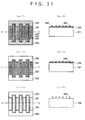
- Fig. 28 shows doubly-supported beams (wherein proximal ends of the fine wires have different shapes on the two lateral sides of each fine wire) functioning as probes composed of silicon fine wires according to an embodiment of the present invention.
- Fig. 28(a) is a perspective view thereof
- Fig. 28(b) is a plan view thereof
- Fig. 28(c) is a cross-sectional view taken along line G-G in Fig. 28(b).
- reference numeral 1001 indicates a handling wafer
- reference numeral 1002 indicates a buried oxide film
- reference numeral 1003 indicates an SOI layer
- reference numeral 1006 indicates silicon fine wires (doubly-supported beams) in which the proximal ends have different shapes on the two lateral sides of each fine wire, the silicon fine wires being formed by utilizing the crystallinity of the SOI layer 1003.
- the silicon fine wires (doubly-supported beams) 1006 having different shapes on the two lateral sides of each fine wire can be produced inexpensively by a simple process that omits a step of forming a silicon oxide film.
- These doubly-supported beams have a durable structure because the proximal ends of each doubly-supported beam have an asymmetrical shape. Accordingly, doubly-supported beams having durability against aging, not being easily broken, and utilizing the crystallinity of silicon can be formed.
- the present invention provides the following advantages.
- the present invention is suitable for reading out very high-density information, measuring mechanical or physical properties of minute samples, and measuring magnetism or atomic force with high resolution.
- the present invention is particularly useful as a measurement technology on the order of nanometers.
Landscapes
- Physics & Mathematics (AREA)
- Health & Medical Sciences (AREA)
- General Health & Medical Sciences (AREA)
- General Physics & Mathematics (AREA)
- Nuclear Medicine, Radiotherapy & Molecular Imaging (AREA)
- Radiology & Medical Imaging (AREA)
- Micromachines (AREA)
- Crystals, And After-Treatments Of Crystals (AREA)
- Measuring Magnetic Variables (AREA)
Abstract
A three-dimensional structure composed of highly-reliable
silicon ultrafine wires, a method for producing the
three-dimensional structure, and a device including the same
are provided. The three-dimensional structure composed of
silicon fine wires includes wires (2) on the order of
nanometers to micrometers formed by wet etching utilizing
the crystallinity of a single-crystal material.
Description
The present invention relates to a three-dimensional
structure composed of silicon fine wires. In particular,
the present invention relates to a three-dimensional
structure using wires on the order of nanometers (referred
to as nano) to micrometers formed by etching utilizing the
crystallinity of silicon etc. as elements, a method for
producing the same, and a device including the same.
Conventionally, a plate or block structure composed of
silicon or a structure formed by bending a metal conducting
wire provides elements such as oscillators and coils.
In general, a tip magnetized with cobalt or iron etc.
is used as a tip of an atomic force microscope to detect a
magnetic field.
Furthermore, the present inventors have already
proposed elements such as a cantilever composed of a fine
three-dimensional structure in the following Patent Document
1 etc.
Japanese Unexamined Patent Application Publication No. 2001-91441 (pp. 7-8, Fig. 4)
Japanese Unexamined Patent Application Publication No. 2001-289768 (pp. 3-4, Fig. 1)
Japanese Unexamined Patent Application Publication No. 2003-114182 (pp. 5-6, Fig. 1)
However, with the known fine tip described above, in-process
control of the magnetic force is impossible.
In a scanning temperature microscope, a loop used as
the temperature sensing element is produced by hand or by
nanofabrication piece by piece. Therefore, confirmation
tests and multipoint measurements are difficult to achieve.
Furthermore, a plate-shaped cantilever used in a known
scanning force microscope within a scanning electron
microscope causes the following problems: When scanning
electron microscopy observation is performed perpendicularly
to the sample, the cantilever blocks the observation point,
so that it is difficult to observe the sample, and to
identify the observation point.
It is expected that miniaturization of the cantilever
using a three-dimensional structure composed of silicon fine
wires will improve the sensitivity in mass spectrometry and
force detection. However, in this technology, damage such
as crystal defects in the vicinity of the surface
significantly affects the Q factor as a mechanical
oscillator. Such damage in the vicinity of the surface must
be reduced. In particular, when the three-dimensional
structure composed of silicon fine wires is formed by
reactive ion etching (anisotropic etching), the damage such
as crystal defects is increased. Therefore, it is important
to study etching techniques.
In view of the above situation, it is an object of the
present invention to provide a highly-reliable three-dimensional
structure composed of silicon ultrafine wires, a
method for producing the same, and a device including the
same.
In order to achieve the above object, the present
invention provides the following:
In other words, the present invention provides the
following features:
Embodiments of the present invention will now be
described with reference to the drawings.
Fig. 1 is a schematic view of a device having a tip
supported by a plurality of fine wires according to an
embodiment of the present invention.
In this figure, reference numeral 1 indicates a
cantilever base, reference numeral 2 indicates a plurality
of fine wires, reference numeral 3 indicates a tip, and
reference numeral 4 indicates a sample.
As shown in the figure, since the tip 3 is supported by
a plurality of fine wires [on the order of nanometers
(hereinafter abbreviated as nano) to micrometers], the
observation portion of the sample 4 is not blocked. As a
result, the portion being observed with the tip 3 can be
readily observed with an optical microscope or a scanning
microscope.
The present inventors have already proposed a fine
mechanical oscillator formed using a semiconductor material,
a method for producing the same, and a measuring device
including the same in the above-cited Patent Document 1.
Fig. 2 is a perspective view of an oscillator (device)
having a tip supported by a plurality of fine wires
according to an embodiment of the present invention.
In this figure, reference numeral 100 indicates an
oscillator base, reference numerals 101 and 102 indicate two
fine wires, and reference numeral 103 indicates a tip formed
at the intersection of the two fine wires 101 and 102.
Fig. 3 is a perspective view of a fine coil (device)
composed of a plurality of fine wires according to an
embodiment of the present invention.
In this figure, reference numeral 200 indicates a fine
coil base, and reference numeral 201 indicates a fine coil
composed of V-shaped fine wires.
Fig. 4 is a perspective view of an oscillator (device)
having tips supported by two doubly-supported fine wires
according to an embodiment of the present invention.
In this figure, reference numeral 300 indicates
oscillator bases disposed at both sides, reference numerals
301 and 302 indicate two fine wires extending from the
oscillator bases 300 disposed at both sides thereof,
respectively, and reference numeral 303 indicates tips
formed at the intersection of the two fine wires 301 and 302.
Alternatively, double coils composed of the two doubly-supported
fine wires may be formed without forming the tips
303 shown in Fig. 4.
Fig. 5 is a perspective view of a fine coil (device)
having a grid structure composed of fine wires according to
an embodiment of the present invention.
In this figure, reference numeral 400 indicates a fine
coil base, and reference numeral 401 indicates a fine coil
having a grid structure composed of fine wires. This device
can also be formed in three-dimensional structure.
Fig. 6, according to an embodiment of the present
invention, is a perspective view of an oscillator (device)
having a tip supported by a plurality of fine wires and used
to detect the temperature-dependent resistance variation.
Fig. 7 is a drawing showing a resistance bridge thereof.
In this figure, reference numeral 500 indicates a
cantilever support, reference numeral 501 indicates a
plurality of fine wires, and reference numeral 502 indicates
a tip.
In this embodiment, each of the cantilevers composed of
the fine wires 501 is doped with boron to provide electrical
conductivity. In addition, the resistance bridge shown in
Fig. 7 is formed at the cantilever support 500. As a result,
the resistance variation due to the temperature of the
cantilever can be detected. Because of the significantly
low heat capacity, this device can provide high sensitivity
and response frequency. In Fig. 7, symbol r1 represents the
resistance of a plurality of the fine wire portions, and
symbol r2 and symbol r3 represent the resistances of the
cantilever support 500.
According to a method for producing the above devices
shown in Figs. 2 to 6, for example, single-crystal silicon
is etched with potassium hydroxide (KOH) to provide a fine
wire composed of a plurality of crystal faces. An example
of such a fine wire is composed of two silicon {111}
surfaces and a silicon {100} surface.
Silicon single-crystals have the {111} surface and its
equivalent surfaces disposed in two or more directions.
Therefore, depending on the combination of the crystal faces,
a fine wire having different axial directions can be
produced by etching the single-crystal silicon.
Furthermore, depending on the combination of fine wires
having different orientations and fine wires parallel to
each other, a one-dimensional line and various two or three-dimensional
structures, such as a coil structure, a grid
structure, a network structure, and an oscillator structure,
can be achieved. Such a three-dimensional structure is
produced using a multilayered structure composed of, for
example, silicon and silicon oxide by masking appropriate
areas according to whether the areas are to be etched or not.
The structures produced by the present invention can be
used as a beam, a V-shaped coil, a V-shaped resistor, a grid
structure, and a three-dimensionally linked structure. In
any case, in known methods, these structures are made by
hand or by combining plate-shaped components. In contrast,
the present invention provides the following advantages:
The structure can be miniaturized, a plurality of the
structures can be produced at the same time, the structure
can be produced with high uniformity, the structure can be
produced three-dimensionally, the frequency of the structure
can be increased, and oscillation loss of the structure can
be decreased.
The above beam can be used as a stylus, a singly-supported
beam, or a probe. The V-shaped coil can be used
as a fine coil.
The V-shaped resistor can be used as a probe for
temperature mapping in a minute area by utilizing the
temperature-dependent resistance variation.
The grid structure can be used as a physical filter or
a physical and chemical filter by modifying the surface
thereof. In addition, the grid structure, which is a kind
of sponge structure, can achieve a predetermined elasticity,
and functions as a filter that selects light depending on
the direction or the wavelength. Furthermore, when the
structure is vibrated, the structure functions as an optical
modulation element. The absorption of a specific substance
can be detected as a change in vibration characteristics of
the structure by combining the filter function of the
specific substance with the oscillator function.
In the structure composed of fine wires, the inside of
the fine wires is used as a waveguide for light or a
waveguide for oscillation, thereby controlling the
propagation of the light or the oscillation.
As described above, fine wires on the order of nano to
micrometers can be achieved by wet etching utilizing the
crystallinity of silicon etc., and a three-dimensional
structure using the fine wires as elements can be achieved.
This technology allows elements such as an oscillator, a net,
a coil, a heat-generating loop, a filter, and a magnetic
sensor on the order of microns to submicrons to be produced.
As a result, the oscillator can detect force or mass,
the net can trap a sample having a specific particle size,
the coil can generate a fine magnetic field or can detect
such a magnetic field, and the heat-generating loop can
measure the temperature distribution of a sample.
This method is applicable to mass production of a
three-dimensional structure composed of millions to hundreds
of millions of fine wires.
Fig. 8 is a schematic view of a fine coil (device) to
which a modulation function can be added, according to an
embodiment of the present invention.
In this figure, reference numeral 600 indicates a fine
coil support, reference numeral 601 indicates a fine coil
composed of fine wires, and reference numeral 602 indicates
a sample.
In this embodiment, when current flows in the fine coil
601 composed of fine wires, the fine coil 601 can detect the
Lorentz force or its gradient due to the magnetic field of
the sample 602 as a force applied in the oscillation
direction.
This device allows a magnetic profile to be measured
without using the characteristics of a magnetic tip.
Furthermore, a modulation function such as modulation of the
current, which cannot be added to known magnetic tips, can
be added to this device.
The present invention is applicable to a scanning probe
microscope, oscillation measurement, analysis of
characteristics of surfaces and interfaces, an electric
circuit, a mass detector, an electrical circuit network, a
substance-trapping filter, and an elastic material. The
present invention is also applicable to the measurements of
temperature, the temperature distribution of electronic
devices, and the temperature distribution and metabolism of
biological materials.
In the following aspect of the present invention, the
wording "a cantilever" generally represents a cantilever
used in an atomic force microscope, and the wording "a
probe" represents a probe which is not limited to the
cantilever used in the atomic force microscope, but
represents an element used for various applications such as
mass detection and magnetic field detection.
Fig. 9 shows cantilevers functioning as probes composed
of silicon fine wires according to an embodiment of the
present invention. Fig. 9(a) is a perspective view thereof,
Fig. 9(b) is a plan view thereof, and Fig. 9(c) is a cross-sectional
view taken along line L-L in Fig. 9(b).
In this figure, reference numeral 701 indicates a
handling wafer, reference numeral 702 indicates a buried
oxide film, reference numeral 703 indicates a silicon-on-insulator
(SOI) layer, and reference numeral 707 indicates
silicon fine wires (cantilevers composed of singly-supported
beams), which are formed by utilizing the crystallinity of
the SOI layer 703.
A method for producing the cantilevers (singly-supported
beams composed of fine wires) will now be
described with reference to Figs. 10 to 14.
As described above, the method for producing a three-dimensional
structure composed of silicon fine wires
includes the steps of preparing an SOI substrate having a
surface composed of the {100} surface of silicon single-crystals
thereon; forming a silicon oxide film 704 on a part
of an SOI layer 703 of the SOI substrate; forming a silicon
nitride film 705 on the SOI layer 703 and the silicon oxide
film 704; removing a part of the silicon nitride film 705 to
expose the SOI layer 703 such that elongated shapes are
repeatedly arranged side-by-side so as to be parallel to the
<110> direction; removing the exposed SOI layer 703 by wet
etching with an alkaline solution; thermally oxidizing the
{111} surfaces 703A exposed by the wet etching to form a
thermally-oxidized film 706; removing a part of the
remaining silicon nitride film 705; wet etching the newly
exposed SOI layer 703 with an alkaline solution; removing
the thermally-oxidized film 706 of the resultant SOI layers
703' having a substantially triangular cross-section, the
remaining silicon nitride film 705, and the silicon oxide
film 704; forming an array of silicon fine wires; processing
the silicon fine wires such that the silicon fine wires have
a predetermined length; and removing a buried oxide film 702
of the SOI substrate to form silicon fine wires [cantilevers
(singly-supported beams composed of fine wires)] 707 that
can be independently oscillated.
Fig. 15 shows cantilevers functioning as probes
composed of silicon fine wires according to a first
modification of the embodiment of the present invention.
Fig. 15(a) is a perspective view thereof, Fig. 15(b) is a
plan view thereof, and Fig. 15(c) is a cross-sectional view
taken along line M-M in Fig. 15(b).
In this embodiment, proximal ends of the silicon fine
wires [cantilevers (singly-supported beams composed of fine
wires)] 708 are aligned. However, the silicon fine wires
708 are formed such that the length of each fine wire
gradually changes from one to the next. Other structures
are the same as those of the above silicon fine wires.
Fig. 16 shows cantilevers functioning as probes
composed of silicon fine wires according to a second
modification of the embodiment of the present invention.
Fig. 16(a) is a perspective view thereof, Fig. 16(b) is a
plan view thereof, and Fig. 16(c) is a cross-sectional view
taken along line N-N in Fig. 16(b).
In this embodiment, distal ends of silicon fine wires
[cantilevers (singly-supported beams composed of fine
wires)] 709 are formed on the same line, whereas the
proximal ends of the silicon fine wires form a slanted shape.
As a result, the length of each fine wire gradually changes
from one to the next. Other structures are the same as
those of the above silicon fine wires.
As described above, according to the present invention,
singly-supported beams composed of silicon fine wires that
suffer no damage such as crystal defects can be formed by
utilizing the crystallinity of silicon, in contrast to a
known example in which cantilevers are formed by anisotropic
etching (such as RIE) regardless of the crystallinity of
silicon.
Fig. 17 shows cantilevers functioning as probes
composed of silicon fine wires according to an embodiment of
the present invention. Fig. 17(a) is a perspective view
thereof, Fig. 17(b) is a plan view thereof, and Fig. 17(c)
is a cross-sectional view taken along line H-H in Fig. 17(b).
In this figure, reference numeral 801 indicates a
handling wafer, reference numeral 802 indicates a buried
oxide film, reference numeral 803 indicates an SOI layer,
and reference numeral 806 indicates silicon fine wires
(cantilevers composed of singly-supported beams), which are
formed by utilizing the crystallinity of the SOI layer 803.
A method for producing the cantilevers (singly-supported
beams in which proximal ends of the fine wires
have different shapes on the two lateral sides of each fine
wire) will now be described with reference to Figs. 18 to 20.
Fig. 21 shows cantilevers functioning as probes
composed of silicon fine wires according to a modification
of the embodiment of the present invention. Fig. 21(a) is a
perspective view thereof, Fig. 21(b) is a plan view thereof,
and Fig. 21(c) is a cross-sectional view taken along line I-I
in Fig. 21(b).
In this embodiment, proximal ends of silicon fine wires
[cantilevers (singly-supported beams composed of fine
wires)] 807 have different shapes on the two lateral sides
of each fine wire. Furthermore, the silicon fine wires
[cantilevers (singly-supported beams composed of fine
wires)] 807 are formed such that the length of each fine
wire gradually changes from one to the next. Other
structures are the same as those of the above silicon fine
wires.
As described above, the singly-supported beams 806 and
807 in which the proximal ends of the fine wires functioning
as probes have different shapes on the two lateral sides of
each fine wire can be produced inexpensively by a simple
process that omits a step of forming a silicon oxide film.
These singly-supported beams have a durable structure
because the proximal ends of the singly-supported beams have
an asymmetrical shape. Accordingly, singly-supported beams
having durability against aging, not being easily broken,
and utilizing the crystallinity of silicon can be formed.
Fig. 22 shows doubly-supported beams functioning as
probes composed of silicon fine wires according to an
embodiment of the present invention. Fig. 22(a) is a
perspective view thereof, Fig. 22(b) is a plan view thereof,
and Fig. 22(c) is a cross-sectional view taken along line K-K
in Fig. 22(b).
In this figure, reference numeral 901 indicates a
handling wafer, reference numeral 902 indicates a buried
oxide film, reference numeral 903 indicates an SOI layer,
and reference numeral 907 indicates silicon fine wires
(doubly-supported beams), which are formed by utilizing the
crystallinity of the SOI layer 903.
A method for producing the doubly-supported beams
composed of fine wires will now be described with reference
to Figs. 23 to 26.
As described above, the method for producing a three-dimensional
structure composed of silicon fine wires
includes the steps of preparing an SOI substrate having a
surface composed of the {100} surface of silicon single-crystals
thereon; forming a silicon oxide film 904 on both
ends of an SOI layer 903 of the SOI substrate; forming a
silicon nitride film 905 on the silicon oxide film 904;
removing a part of the silicon nitride film 905 to expose
the SOI layer 903 such that elongated shapes are repeatedly
arranged side-by-side so as to be parallel to the <110>
direction; removing the exposed SOI layer 903 by wet etching
with an alkaline solution; thermally oxidizing the {111}
surfaces 903A exposed by the wet etching; removing all of
the remaining silicon nitride film 905; wet etching the
newly exposed SOI layer 903 with an alkaline solution;
forming an array of silicon fine wires; and removing a
buried oxide film 902 of the SOI substrate to form silicon
fine wires 907 that can be independently oscillated.
Fig. 27 shows doubly-supported beams of fine wires
functioning as probes composed of silicon fine wires
according to a modification of the embodiment of the present
invention. Fig. 27(a) is a perspective view thereof, Fig.
27(b) is a plan view thereof, and Fig. 27(c) is a cross-sectional
view taken along line L-L in Fig. 27(b).
In this embodiment, the doubly-supported beams composed
of fine wires 908 are formed such that the length of each
fine wire gradually changes from one to the next. Other
structures are the same as those of the above silicon fine
wires.
As described above, according to the present invention,
doubly-supported beams composed of silicon fine wires that
suffer no damage such as crystal defects can be formed by
utilizing the crystallinity of silicon, in contrast to a
known method in which doubly-supported beams are formed by
anisotropic etching (such as RIE) regardless of the
crystallinity of silicon.
Fig. 28 shows doubly-supported beams (wherein proximal
ends of the fine wires have different shapes on the two
lateral sides of each fine wire) functioning as probes
composed of silicon fine wires according to an embodiment of
the present invention. Fig. 28(a) is a perspective view
thereof, Fig. 28(b) is a plan view thereof, and Fig. 28(c)
is a cross-sectional view taken along line G-G in Fig. 28(b).
In this figure, reference numeral 1001 indicates a
handling wafer, reference numeral 1002 indicates a buried
oxide film, reference numeral 1003 indicates an SOI layer,
and reference numeral 1006 indicates silicon fine wires
(doubly-supported beams) in which the proximal ends have
different shapes on the two lateral sides of each fine wire,
the silicon fine wires being formed by utilizing the
crystallinity of the SOI layer 1003.
A method for producing the doubly-supported beams
composed of fine wires will now be described with reference
to Figs. 29 to 31.
As described above, the silicon fine wires (doubly-supported
beams) 1006 having different shapes on the two
lateral sides of each fine wire can be produced
inexpensively by a simple process that omits a step of
forming a silicon oxide film. These doubly-supported beams
have a durable structure because the proximal ends of each
doubly-supported beam have an asymmetrical shape.
Accordingly, doubly-supported beams having durability
against aging, not being easily broken, and utilizing the
crystallinity of silicon can be formed.
The present invention is not limited to the above
embodiments. Various modifications can be made based on the
purpose of the present invention, and those modifications
are not excluded from the scope of the present invention.
As described above in detail, the present invention
provides the following advantages.
The present invention is suitable for reading out very
high-density information, measuring mechanical or physical
properties of minute samples, and measuring magnetism or
atomic force with high resolution. The present invention is
particularly useful as a measurement technology on the order
of nanometers.
Claims (31)
- A three-dimensional structure composing silicon fine wires comprising fine wires on the order of nanometers to micrometers formed by wet etching utilizing the crystallinity of a single-crystal material.
- The three-dimensional structure composing silicon fine wires according to claim 1, being a fine coil comprising a plurality of the wires.
- A device comprising a three-dimensional structure composing silicon fine wires, wherein a magnetic field is generated or detected with a fine coil comprising a plurality of fine wires on the order of nanometers to micrometers formed by wet etching utilizing the crystallinity of a single-crystal material.
- A device comprising a three-dimensional structure composing silicon fine wires, wherein the temperature in a minute area is measured using the temperature-dependent resistance variation of a fine coil comprising a plurality of fine wires on the order of nanometers to micrometers formed by wet etching utilizing the crystallinity of a single-crystal material.
- The device comprising a three-dimensional structure composing silicon fine wires according to claim 4, wherein the fine coil is used in visualization of the temperature distribution of planar samples, visualization of the temperature distribution and metabolism of biological materials, and mapping of the temperature distribution of electronic devices.
- A device comprising a three-dimensional structure composing silicon fine wires, wherein the interaction or the change in force or mass on the atomic level is detected utilizing the change in amplitude, phase, or self-excited frequency of an oscillator comprising a plurality of fine wires on the order of nanometers to micrometers formed by wet etching utilizing the crystallinity of a single-crystal material.
- A device comprising a three-dimensional structure composing silicon fine wires, wherein a sample having a specific particle size is trapped in a network structure comprising a plurality of fine wires on the order of nanometers to micrometers formed by wet etching utilizing the crystallinity of a single-crystal material.
- The device comprising a three-dimensional structure composing silicon fine wires according to claim 7, being a filter to absorb a specific substance, the filter being formed by modifying the surface of the network structure.
- The device comprising a three-dimensional structure composing silicon fine wires according to claim 7, wherein the network structure is an elastic body as a whole so that the structure is elastic.
- The device comprising a three-dimensional structure composing silicon fine wires according to claim 7, wherein the network structure is a three-dimensional optical filter, a grating, or a shielding window.
- The device comprising a three-dimensional structure composing silicon fine wires according to claim 7, wherein the network structure is a resistor having a grid structure, thereby providing an electrical circuit network.
- A device comprising a three-dimensional structure composing silicon fine wires, wherein the three-dimensional structure comprises a plurality of fine wires on the order of nanometers to micrometers formed by wet etching utilizing the crystallinity of a single-crystal material, and a tip or a block formed at an intersection of the fine wires by the wet etching is used as a probe or a mass to provide the structure with predetermined vibration characteristics.
- A device comprising a three-dimensional structure composing silicon fine wires, wherein the device comprises a microscope tip with which an observation portion is readily observed, the tip comprising a plurality of fine wires on the order of nanometers to micrometers formed by wet etching utilizing the crystallinity of a single-crystal material.
- A method for producing a three-dimensional structure composing silicon fine wires, the method comprising the steps of:(a) preparing a silicon-on-insulator (SOI) substrate having a surface composed of the {100} surface of silicon single-crystals thereon;(b) forming a silicon oxide film on a part of an SOI layer of the SOI substrate;(C) forming a silicon nitride film on the silicon oxide film and the a part of the SOI layer;(d) removing a part of the silicon nitride film to expose the SOI layer such that elongated shapes are repeatedly arranged so as to be parallel to the <110> direction;(e) removing the exposed SOI layer portions by wet etching;(f) thermally oxidizing the {111} surface exposed by the wet etching to form a thermally-oxidized film;(g) removing a part of the remaining silicon nitride film and wet etching the newly exposed SOI layer to form an array of silicon fine wires; and(h) removing a buried oxide film of the SOI substrate to form silicon fine wires that can be independently oscillated.
- The method for producing a three-dimensional structure composing silicon fine wires according to claim 14, wherein proximal ends of the silicon fine wires are formed so as to have different shapes on the two lateral sides of each fine wire.
- The method for producing a three-dimensional structure composing silicon fine wires according to claim 14, wherein the silicon fine wires are processed such that each fine wire has the same length.
- The method for producing a three-dimensional structure comprising silicon fine wires according to claim 14, wherein the silicon fine wires are processed such that each fine wire has different length.
- A method for producing a three-dimensional structure composing silicon fine wires, the method comprising the steps of:(a) preparing an SOI substrate having a surface composed of the {100} surface of silicon single-crystals thereon;(b) forming a silicon nitride film on an SOI layer of the SOI substrate;(c) removing a part of the silicon nitride film to expose the SOI layer such that elongated shapes are repeatedly arranged so as to be parallel to the <110> direction;(d) removing the exposed SOI layer portions by wet etching;(e) thermally oxidizing the {111} surface exposed by the wet etching to form a thermally-oxidized film;(f) removing a part of the remaining silicon nitride film and wet etching the newly exposed SOI layer to form an array of silicon fine wires; and(g) removing a buried oxide film of the SOI substrate to form silicon fine wires that can be independently oscillated.
- The method for producing a three-dimensional structure composing silicon fine wires according to claim 18, wherein proximal ends of the silicon fine wires are formed so as to have different shapes on the two lateral sides of each fine wire.
- The method for producing a three-dimensional structure composing silicon fine wires according to claim 18, wherein the silicon fine wires are processed such that each fine wire has the same length.
- The method for producing a three-dimensional structure composing silicon fine wires according to claim 18, wherein the silicon fine wires are processed such that each fine wire has different length.
- The method for producing a three-dimensional structure composing silicon fine wires according to claim 14, wherein the three-dimensional structure comprises probes.
- The method for producing a three-dimensional structure composing silicon fine wires according to claim 22, wherein the probes are singly-supported beams.
- The method for producing a three-dimensional structure composing silicon fine wires according to claim 23, wherein the singly-supported beams are cantilevers for an atomic force microscope.
- The method for producing a three-dimensional structure composing silicon fine wires according to claim 22, wherein the probes are doubly-supported beams.
- The method for producing a three-dimensional structure composing silicon fine wires according to claim 18, wherein the three-dimensional structure comprises probes.
- The method for producing a three-dimensional structure composing silicon fine wires according to claim 26, wherein the probes are singly-supported beams.
- The method for producing a three-dimensional structure composing silicon fine wires according to claim 27, wherein the singly-supported beams are cantilevers for an atomic force microscope.
- The method for producing a three-dimensional structure composing silicon fine wires according to claim 26, wherein the probes are doubly-supported beams.
- A three-dimensional structure composing silicon fine wires produced by the method for producing a three-dimensional structure comprising silicon fine wires according to claim 14.
- A three-dimensional structure composing silicon fine wires produced by the method for producing a three-dimensional structure comprising silicon fine wires according to claim 18.
Applications Claiming Priority (5)
| Application Number | Priority Date | Filing Date | Title |
|---|---|---|---|
| JP2002161140 | 2002-06-03 | ||
| JP2002161140 | 2002-06-03 | ||
| JP2003151255 | 2003-05-28 | ||
| JP2003151255A JP2004058267A (en) | 2002-06-03 | 2003-05-28 | Three-dimensional structure made of silicon fine wire, method of manufacturing the same, and apparatus using the same |
| PCT/JP2003/006929 WO2003102549A1 (en) | 2002-06-03 | 2003-06-02 | Three-dimensional structural body composed of silicon fine wire, its manufacturing method, and device using same |
Publications (2)
| Publication Number | Publication Date |
|---|---|
| EP1510806A1 true EP1510806A1 (en) | 2005-03-02 |
| EP1510806A4 EP1510806A4 (en) | 2008-03-19 |
Family
ID=29714325
Family Applications (1)
| Application Number | Title | Priority Date | Filing Date |
|---|---|---|---|
| EP03730767A Withdrawn EP1510806A4 (en) | 2002-06-03 | 2003-06-02 | THREE-DIMENSIONAL STRUCTURAL BODY MADE OF A THIN SILICON FILM, MANUFACTURING METHOD AND DEVICE USING SUCH BODY |
Country Status (6)
| Country | Link |
|---|---|
| US (2) | US7297568B2 (en) |
| EP (1) | EP1510806A4 (en) |
| JP (1) | JP2004058267A (en) |
| KR (1) | KR100698820B1 (en) |
| RU (1) | RU2320976C2 (en) |
| WO (1) | WO2003102549A1 (en) |
Cited By (2)
| Publication number | Priority date | Publication date | Assignee | Title |
|---|---|---|---|---|
| CN103335754A (en) * | 2013-06-19 | 2013-10-02 | 合肥工业大学 | Fully-flexible three-dimensional force tactile sensor |
| CN103700760A (en) * | 2014-01-14 | 2014-04-02 | 东南大学 | Volume preparation device of micro-nano thermocouple probe precursors |
Families Citing this family (12)
| Publication number | Priority date | Publication date | Assignee | Title |
|---|---|---|---|---|
| JP2004058267A (en) | 2002-06-03 | 2004-02-26 | Japan Science & Technology Corp | Three-dimensional structure made of silicon fine wire, method of manufacturing the same, and apparatus using the same |
| KR20060036456A (en) * | 2003-07-16 | 2006-04-28 | 도쿠리쓰교세이호징 가가쿠 기주쓰 신코 기코 | Scanning probe microscope probe and its manufacturing method |
| KR100793122B1 (en) * | 2003-08-11 | 2008-01-10 | 도쿠리쓰교세이호징 가가쿠 기주쓰 신코 기코 | Probe for probe microscope using transparent substrate, manufacturing method thereof and probe microscope device |
| JP2006125984A (en) | 2004-10-28 | 2006-05-18 | Japan Science & Technology Agency | Measuring device with daisy type cantilever wheel |
| JP2007069329A (en) * | 2005-09-08 | 2007-03-22 | Japan Science & Technology Agency | Manufacturing method of micro three-dimensional structure operation tool and micro three-dimensional structure operation tool manufactured thereby |
| US8080481B2 (en) * | 2005-09-22 | 2011-12-20 | Korea Electronics Technology Institute | Method of manufacturing a nanowire device |
| KR100943707B1 (en) * | 2007-10-05 | 2010-02-23 | 한국전자통신연구원 | 3D Nano Devices Including Nanostructures |
| JP5553266B2 (en) * | 2008-06-09 | 2014-07-16 | 独立行政法人産業技術総合研究所 | Fabrication method of nanowire field effect transistor |
| CN103021818B (en) * | 2012-12-31 | 2016-04-20 | 中国科学院上海微系统与信息技术研究所 | Conformal microstructure transfer method |
| RU2619811C1 (en) * | 2015-12-22 | 2017-05-18 | Федеральное государственное бюджетное образовательное учреждение высшего образования "Московский государственный университет имени М.В. Ломоносова" (МГУ) | Method of producing elements with nanostructures for local probe systems |
| US10976238B2 (en) * | 2019-01-30 | 2021-04-13 | Xi'an Jiaotong University | Measurement apparatus for micro- and nano-scale material and measurement method thereof |
| CN111398638B (en) * | 2020-03-30 | 2023-05-05 | 哈尔滨工业大学 | Kelvin probe force microscope system and sample side wall scanning method |
Family Cites Families (23)
| Publication number | Priority date | Publication date | Assignee | Title |
|---|---|---|---|---|
| AU596289B2 (en) * | 1987-04-14 | 1990-04-26 | Sumitomo Electric Industries, Ltd. | Method of the production of ceramic superconductor filaments |
| US5171992A (en) * | 1990-10-31 | 1992-12-15 | International Business Machines Corporation | Nanometer scale probe for an atomic force microscope, and method for making same |
| JP3076148B2 (en) * | 1992-06-30 | 2000-08-14 | オリンパス光学工業株式会社 | Cantilever tip for scanning probe microscope |
| JP3308569B2 (en) * | 1991-09-24 | 2002-07-29 | オリンパス光学工業株式会社 | Optical scanning device |
| US5386720A (en) * | 1992-01-09 | 1995-02-07 | Olympus Optical Co., Ltd. | Integrated AFM sensor |
| JP2880014B2 (en) * | 1992-02-25 | 1999-04-05 | 松下電工株式会社 | Silicon substrate etching method |
| US5405454A (en) * | 1992-03-19 | 1995-04-11 | Matsushita Electric Industrial Co., Ltd. | Electrically insulated silicon structure and producing method therefor |
| CA2154357C (en) | 1993-02-04 | 2004-03-02 | Kevin A. Shaw | Microstructures and single-mask, single-crystal process for fabrication thereof |
| US5399415A (en) * | 1993-02-05 | 1995-03-21 | Cornell Research Foundation, Inc. | Isolated tungsten microelectromechanical structures |
| JPH06302513A (en) * | 1993-04-16 | 1994-10-28 | Nippon Steel Corp | Manufacture of single crystal silicon quantum wire |
| JPH0722605A (en) * | 1993-06-22 | 1995-01-24 | Nippon Steel Corp | Quantum wire manufacturing method |
| US6075585A (en) * | 1994-04-12 | 2000-06-13 | The Board Of Trustees Of The Leland Stanford, Jr. University | Vibrating probe for a scanning probe microscope |
| JP3192887B2 (en) * | 1994-09-21 | 2001-07-30 | キヤノン株式会社 | Probe, scanning probe microscope using the probe, and recording / reproducing apparatus using the probe |
| WO1997004283A2 (en) * | 1995-07-20 | 1997-02-06 | Cornell Research Foundation, Inc. | Microfabricated torsional cantilevers for sensitive force detection |
| JPH09229945A (en) * | 1996-02-23 | 1997-09-05 | Canon Inc | METHOD FOR MANUFACTURING AIR BRIDGE STRUCTURE SUPPORTING MICRO STRUCTURE, FEMALE SUBSTRATE THEREOF, AIR BRIDGE STRUCTURE, MICRO STRUCTURE USING THE SAME, AND TUBE CURRENT OR MICRO FORCE DETECTION PROBE |
| US5856967A (en) | 1997-08-27 | 1999-01-05 | International Business Machines Corporation | Atomic force microscopy data storage system with tracking servo from lateral force-sensing cantilever |
| AU1389799A (en) * | 1997-11-07 | 1999-05-31 | California Institute Of Technology | Micromachined membrane particle filter using parylene reinforcement |
| RU2139595C1 (en) * | 1998-03-18 | 1999-10-10 | Научно-исследовательский институт измерительных систем | Method for producing silicon-on-insulator structures |
| KR100329208B1 (en) * | 1998-06-18 | 2002-03-21 | 니시무로 타이죠 | Functional device and a method for manufacturing thereof and an optical disc apparatus using the functional device |
| JP3687030B2 (en) | 1999-06-23 | 2005-08-24 | 独立行政法人科学技術振興機構 | Micro surface temperature distribution measurement method and apparatus therefor |
| JP2001091441A (en) * | 1999-07-16 | 2001-04-06 | Japan Science & Technology Corp | Mechanical vibrator of nanometer order, method of manufacturing the same, and measuring device using the same |
| ATE463462T1 (en) * | 2000-10-09 | 2010-04-15 | Imec | METHOD FOR PRODUCING MICRO-MACHINED ARRANGEMENTS |
| JP2004058267A (en) | 2002-06-03 | 2004-02-26 | Japan Science & Technology Corp | Three-dimensional structure made of silicon fine wire, method of manufacturing the same, and apparatus using the same |
-
2003
- 2003-05-28 JP JP2003151255A patent/JP2004058267A/en active Pending
- 2003-06-02 RU RU2004139083/28A patent/RU2320976C2/en not_active IP Right Cessation
- 2003-06-02 EP EP03730767A patent/EP1510806A4/en not_active Withdrawn
- 2003-06-02 WO PCT/JP2003/006929 patent/WO2003102549A1/en not_active Ceased
- 2003-06-02 KR KR1020047019631A patent/KR100698820B1/en not_active Expired - Fee Related
- 2003-06-02 US US10/515,334 patent/US7297568B2/en not_active Expired - Fee Related
-
2006
- 2006-08-16 US US11/504,715 patent/US20060273445A1/en not_active Abandoned
Cited By (3)
| Publication number | Priority date | Publication date | Assignee | Title |
|---|---|---|---|---|
| CN103335754A (en) * | 2013-06-19 | 2013-10-02 | 合肥工业大学 | Fully-flexible three-dimensional force tactile sensor |
| CN103335754B (en) * | 2013-06-19 | 2015-04-22 | 合肥工业大学 | Fully-flexible three-dimensional force tactile sensor |
| CN103700760A (en) * | 2014-01-14 | 2014-04-02 | 东南大学 | Volume preparation device of micro-nano thermocouple probe precursors |
Also Published As
| Publication number | Publication date |
|---|---|
| US20060273445A1 (en) | 2006-12-07 |
| US7297568B2 (en) | 2007-11-20 |
| EP1510806A4 (en) | 2008-03-19 |
| KR100698820B1 (en) | 2007-03-23 |
| RU2004139083A (en) | 2005-06-10 |
| JP2004058267A (en) | 2004-02-26 |
| US20050247998A1 (en) | 2005-11-10 |
| WO2003102549A1 (en) | 2003-12-11 |
| RU2320976C2 (en) | 2008-03-27 |
| KR20050019111A (en) | 2005-02-28 |
Similar Documents
| Publication | Publication Date | Title |
|---|---|---|
| US7297568B2 (en) | Three-dimensional structural body composed of silicon fine wire, its manufacturing method, and device using same | |
| KR100214152B1 (en) | Piezoresistive cantilever for atomic force microscopy | |
| Carr et al. | Measurement of mechanical resonance and losses in nanometer scale silicon wires | |
| KR100501787B1 (en) | Nanometer-order mechanical vibrator, production method thereof and measuring device using it | |
| CN108027390B (en) | Compact probe for atomic force microscopy and atomic force microscope comprising such a probe | |
| EP1757919A1 (en) | Probe head manufacturing method | |
| US20060011467A1 (en) | Method of manufacturing the multi-tip probe, a multi-tip probe, and surface characteristic analysis apparatus | |
| JP2000065718A (en) | Scanning probe microscope (SPM) probe and SPM device | |
| Nafari et al. | MEMS sensor for in situ TEM atomic force microscopy | |
| US6794296B1 (en) | Aperture in a semiconductor material, and the production and use thereof | |
| JP3675406B2 (en) | Micromaterial testing apparatus and mechanical property evaluation method using the same | |
| US10302673B2 (en) | Miniaturized and compact probe for atomic force microscopy | |
| US9389244B2 (en) | Vertical embedded sensor and process of manufacturing thereof | |
| JP3527947B2 (en) | Probe, manufacturing method thereof, microscope and tester having probe | |
| JP5523497B2 (en) | Micromachine component with cantilever and integrated electrical functional element | |
| JP4931708B2 (en) | Microscope probe and scanning probe microscope | |
| Naeli | Optimization of piezoresistive cantilevers for static and dynamic sensing applications | |
| JPH11271015A (en) | Cantilever tip for scanning probe microscope and method of manufacturing the same | |
| CN101072986A (en) | Metallic thin film piezoresistive transduction in micromechanical and nanomechanical devices and its application in self-sensing spm probes | |
| KR20070011433A (en) | Metal thin film piezo-resistive transducers in micromechanical and nanomechanical devices and their application in self-sensing SPM probes | |
| KR100397090B1 (en) | Electrostatic-type evaluation element for evaluating thin film materials and method manufacturing it | |
| JPH095337A (en) | Cantilever chip and method of manufacturing the same | |
| JP2008089404A (en) | Surface characteristic analysis apparatus, surface characteristic analysis method, and probe unit | |
| KR20080101455A (en) | Semiconductor probe and manufacturing method | |
| JPH06258017A (en) | Microdisplacement element, and multidisplacement element, tunnel current detector and information processor employing it |
Legal Events
| Date | Code | Title | Description |
|---|---|---|---|
| PUAI | Public reference made under article 153(3) epc to a published international application that has entered the european phase |
Free format text: ORIGINAL CODE: 0009012 |
|
| 17P | Request for examination filed |
Effective date: 20041207 |
|
| AK | Designated contracting states |
Kind code of ref document: A1 Designated state(s): AT BE BG CH CY CZ DE DK EE ES FI FR GB GR HU IE IT LI LU MC NL PT RO SE SI SK TR |
|
| RBV | Designated contracting states (corrected) |
Designated state(s): CH DE FR GB LI |
|
| A4 | Supplementary search report drawn up and despatched |
Effective date: 20080218 |
|
| STAA | Information on the status of an ep patent application or granted ep patent |
Free format text: STATUS: THE APPLICATION HAS BEEN WITHDRAWN |
|
| 18W | Application withdrawn |
Effective date: 20080326 |