EP1510054B1 - Method and apparatus for coupling a device to a bus - Google Patents
Method and apparatus for coupling a device to a bus Download PDFInfo
- Publication number
- EP1510054B1 EP1510054B1 EP03731492A EP03731492A EP1510054B1 EP 1510054 B1 EP1510054 B1 EP 1510054B1 EP 03731492 A EP03731492 A EP 03731492A EP 03731492 A EP03731492 A EP 03731492A EP 1510054 B1 EP1510054 B1 EP 1510054B1
- Authority
- EP
- European Patent Office
- Prior art keywords
- bus
- coupling
- coupler
- coupling strength
- characteristic
- Prior art date
- Legal status (The legal status is an assumption and is not a legal conclusion. Google has not performed a legal analysis and makes no representation as to the accuracy of the status listed.)
- Expired - Lifetime
Links
- 230000008878 coupling Effects 0.000 title claims description 88
- 238000010168 coupling process Methods 0.000 title claims description 88
- 238000005859 coupling reaction Methods 0.000 title claims description 88
- 238000000034 method Methods 0.000 title claims 6
- 125000006850 spacer group Chemical group 0.000 claims description 12
- 230000004044 response Effects 0.000 claims description 8
- 230000035699 permeability Effects 0.000 claims description 6
- 239000000463 material Substances 0.000 description 9
- 238000004519 manufacturing process Methods 0.000 description 6
- 230000008901 benefit Effects 0.000 description 4
- 230000008859 change Effects 0.000 description 3
- 230000000694 effects Effects 0.000 description 3
- 238000005259 measurement Methods 0.000 description 3
- 238000010586 diagram Methods 0.000 description 2
- 238000000926 separation method Methods 0.000 description 2
- 229910002244 LaAlO3 Inorganic materials 0.000 description 1
- 229920000106 Liquid crystal polymer Polymers 0.000 description 1
- 239000004977 Liquid-crystal polymers (LCPs) Substances 0.000 description 1
- 229910010252 TiO3 Inorganic materials 0.000 description 1
- 230000004075 alteration Effects 0.000 description 1
- 230000006399 behavior Effects 0.000 description 1
- 230000000593 degrading effect Effects 0.000 description 1
- 238000001514 detection method Methods 0.000 description 1
- 239000003989 dielectric material Substances 0.000 description 1
- 238000009826 distribution Methods 0.000 description 1
- 230000005684 electric field Effects 0.000 description 1
- 230000006870 function Effects 0.000 description 1
- 239000002223 garnet Substances 0.000 description 1
- 230000001939 inductive effect Effects 0.000 description 1
- MTRJKZUDDJZTLA-UHFFFAOYSA-N iron yttrium Chemical compound [Fe].[Y] MTRJKZUDDJZTLA-UHFFFAOYSA-N 0.000 description 1
- 230000007246 mechanism Effects 0.000 description 1
- 210000003205 muscle Anatomy 0.000 description 1
- 230000003068 static effect Effects 0.000 description 1
- 239000000758 substrate Substances 0.000 description 1
- 230000008685 targeting Effects 0.000 description 1
Images
Classifications
-
- H—ELECTRICITY
- H04—ELECTRIC COMMUNICATION TECHNIQUE
- H04L—TRANSMISSION OF DIGITAL INFORMATION, e.g. TELEGRAPHIC COMMUNICATION
- H04L25/00—Baseband systems
- H04L25/02—Details ; arrangements for supplying electrical power along data transmission lines
-
- H—ELECTRICITY
- H01—ELECTRIC ELEMENTS
- H01P—WAVEGUIDES; RESONATORS, LINES, OR OTHER DEVICES OF THE WAVEGUIDE TYPE
- H01P5/00—Coupling devices of the waveguide type
- H01P5/12—Coupling devices having more than two ports
- H01P5/16—Conjugate devices, i.e. devices having at least one port decoupled from one other port
- H01P5/18—Conjugate devices, i.e. devices having at least one port decoupled from one other port consisting of two coupled guides, e.g. directional couplers
- H01P5/184—Conjugate devices, i.e. devices having at least one port decoupled from one other port consisting of two coupled guides, e.g. directional couplers the guides being strip lines or microstrips
- H01P5/185—Edge coupled lines
-
- H—ELECTRICITY
- H01—ELECTRIC ELEMENTS
- H01P—WAVEGUIDES; RESONATORS, LINES, OR OTHER DEVICES OF THE WAVEGUIDE TYPE
- H01P5/00—Coupling devices of the waveguide type
- H01P5/12—Coupling devices having more than two ports
-
- H—ELECTRICITY
- H04—ELECTRIC COMMUNICATION TECHNIQUE
- H04L—TRANSMISSION OF DIGITAL INFORMATION, e.g. TELEGRAPHIC COMMUNICATION
- H04L12/00—Data switching networks
- H04L12/28—Data switching networks characterised by path configuration, e.g. LAN [Local Area Networks] or WAN [Wide Area Networks]
- H04L12/40—Bus networks
-
- H—ELECTRICITY
- H04—ELECTRIC COMMUNICATION TECHNIQUE
- H04L—TRANSMISSION OF DIGITAL INFORMATION, e.g. TELEGRAPHIC COMMUNICATION
- H04L25/00—Baseband systems
- H04L25/02—Details ; arrangements for supplying electrical power along data transmission lines
- H04L25/0264—Arrangements for coupling to transmission lines
- H04L25/0266—Arrangements for providing Galvanic isolation, e.g. by means of magnetic or capacitive coupling
Definitions
- This description relates to controlling coupling strength in electromagnetic bus coupling.
- Electromagnetic couplers can be used, for example, to couple data between electronic devices and a communication bus (e.g., a multi-drop bus) in place of more conventional direct electrical connections.
- a communication bus e.g., a multi-drop bus
- Such an arrangement is proposed in United States Patent 5,638,402 .
- the coupling strength of a coupler depends on physical characteristics of the elements that make up the coupler.
- US2001/0020875 discloses an apparatus wherein a controller sends signals to an electromagnetic coupler (Cl,..,Cn) associated with a bus (301,303), the signals being arranged to set a coupling strength of the coupler in response to a changing data pattern (fig. 4a: CALword) on control lines (B1,B2,..,Bn) from the controller, wherein the coupler is to couple signal energy from the bus to a device coupled to the coupler.
- an electromagnetic coupler Cl,..,Cn
- a bus 301,303
- CALword changing data pattern
- the coupling strengths of the couplings between the bus and the communicating devices 224, 226, 228 are all controlled to be uniformly within a targeted range.
- One way to control the coupling strengths to be uniform is to impose tight manufacturing tolerances on the dimensions and properties of dielectric materials associated with the couplings.
- Controlling coupling strengths to fall uniformly within a particular range achieves a compromise between competing constraints. Excessive coupler strengths cause large impedance disturbances along the bus, thereby degrading signal integrity. High coupler strengths also divert too much signal energy into drop-off points 224 that are closer to the bus master 230, leaving little energy to divert to distant drop-off points 228. On the other hand, insufficient coupler strength causes even the nearest drop-off points to receive or impart too little energy from or to the bus.
- motherboards could include dielectric spacers of different heights glued to the motherboard at the locations of drop-off points along the bus. Or the widths of motherboard coupling traces could be different at different coupler locations.
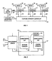
- coupling strengths of a series of electromagnetic bus couplers 10, 12, 14 also can be controlled dynamically by a coupling strength controller 16 to achieve a wide variety of goals.
- the controller provides signals on lines 18, 20, 22 to the couplers to control the coupling strengths and receives information about coupling strengths on lines 24, 26, 28 from the devices 32, 34, 36 that are served by the couplers.
- the devices may include circuitry to measure the amplitudes of incoming signals or to use error detection info in the data stream to measure bit error rate which may be a complex function of the couplers' strengths.
- the controller uses the strength information and information 30 about coupling objectives to generate appropriate control signals to the couplers. The controller can therefore operate as a feedback loop.
- the coupling objectives may relate to the operation of the bus or a bus master 42 or one or more of the devices 32, 34, 36 that communicate through the couplers to a bus 40.
- the coupling objectives could include specific or relative values for the coupling strengths of the respective couplers.
- the bus master could provide information 33 about data that is about to be communicated to respective couplers, and the controller could use that information as the basis for controlling coupling strengths.
- the devices 32, 34, 36 could provide information or instructions 35, 37, 39 that represent coupling objectives to be enforced or taken into account by the controller. The controller could use combinations of coupling objectives in deciding how to control the coupling strengths.
- the controller may include a microprocessor or circuit logic, memory, and algorithms that enable it to use the coupling strategies, target coupling strengths, and measured coupling strengths, to generate control signals.
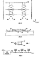
- each of the couplers is characterized by a coupling strength 54 that represents the strength of electromagnetic coupling across a coupler interface 57 between two coupling elements such as two traces, one or both of which may be zigzag traces.
- One of the traces is associated with the bus and the other is associated with a device. The two traces are separated by a small gap.
- the coupling strength represents the extent to which the bus on one hand and a device on the other hand are able to share energy across the interface.
- each of the traces may also be coupled with a reference or ground plane. The various couplings affect the coupling strength between the two traces.
- the coupling strength is determined by a complex set of variables that include, for example, the sizes, shapes, and materials used in fabricating the traces, the reference planes, the spacers between each of the traces and its associated reference plane, and the spacer between the traces, and capacitive and inductive effects associated with the different elements.
- One or more of the elements that make up the coupler have measurable characteristics 56 that represent the coupling strength.
- One of more of the elements also have controllable characteristics 58 that can be used to control the coupling strength of the coupler.
- the measurable characteristics can be determined by a measurement/driver circuit 59 and the information can be fed back to the controller on line 20. The measuring would typically occur in the circuitry of the devices 32, 34, 36.
- the controllable characteristics can be altered by a driver portion of the measurement/driver circuit based on instructions received on line 18 from the controller.
- the measurement/driver circuit could alternatively be part of the controller.
- the coupling strength of a coupler could be measured by sensing the voltage level of a signal that has passed through the coupler and comparing it with a voltage reference value.
- error rates of data that have passed through a coupler could be measured during a period of calibration and the coupling strength could be adjusted to drive the error rate to an acceptably low level. To save time, this scheme might extrapolate error rates from a relatively shorter calibration period with coupling strength settings that produce high error rates which can be measured quickly.
- each coupler can be adjusted electrically to have a coupler strength close to an intended value, thus reducing the effects of manufacturing tolerances.
- configuration-time conditions such as which bus positions are populated and run-time conditions such as temperature and supply voltages can be optimized for by appropriate changes to coupler strength targets.
- coupling strengths may be electrically controlled to suit the particular number of memory slots populated in a given system. If all slots are populated, the coupling strengths could be set to a profile of coupling strengths along the bus which is ideal for that configuration. Without control of coupling strengths, this worst-case profile must always be targeted, within manufacturing accuracy, for each coupler position. With control of coupling strengths, if only a portion of the slots are populated, the coupling strengths of the unpopulated slots could be set extremely low, while the populated slots could be set to coupling strengths including some profile of higher strengths than if all slots are populated.
- the benefit for the system with fewer populated slots may be higher bandwidth, lower error rates, or lower power dissipation. Similar benefits can be obtained in other applications if coupling strengths can be electrically adjusted in response to any measurable device or system condition.
- Feedback control could be used to optimize a bus system at run time for its own bus configuration. Sensors could be provided to determine when a slot is not occupied and that information could be provided to the controller 16.
- Dynamic control also would permit adjusting coupler strengths in response to changing data patterns, for example, from data burst to data burst or even from bus cycle to bus cycle. For example, if the bus master has addressed a particular bus slot for an upcoming read or write operation, it is undesirable to route equal amounts of signal energy to other, un-addressed slots that will not use the information. Instead, the un-addressed slots can be turned off by drastically lowering their coupling strength during the data burst. The effect is to make the presence of the un-addressed slots largely invisible to the bus, or to make the bus look effectively as if it were populated by only one slot, the relevant one. This approach may again result in increased bandwidth, lower error rates, reduced power dissipation, etc.
- coupler characteristics can be used to dynamically and electrically control coupling strength.
- zigzag coupling traces 62, 64 on bus portions of two couplers and zigzag coupling traces 60, 66 on device portions of two couplers are spaced apart by spacers 70, 72.
- the spacers are made of electrically nonlinear (and possibly anisotropic) material in which properties such as permitivity or permeability in the Z direction are influenced by conditions such as a strength of a magnetic field 68 formed in the Y direction.
- YIG yttrium iron garnet
- Such materials are already used to make devices such as isolators, circulators, filters, and current controlled oscillators.
- Electrodes A and B are used to establish a DC field 68 of a selectabie value in direction Y to influence the permitivity or permeability properties of the spacers 70, 72 in direction Z.
- the strength of the field established between electrodes A and B is controlled by controller 16 through the driver.
- the resulting permeability of the spacers along the Z axis determines the coupling strengths of the couplers.
- Another implementation generates fields in the same Z direction as the coupling to alter the electrical behavior of the coupler.
- the properties in direction Z can be directly influenced by a DC bias 80 imposed between the traces 60 and 62 in the Z direction, for each coupler, and controlled by controller 16.
- Varactors for example, are structures in which the capacitance is determined by the DC voltage across the varactor.
- Such DC biasing is effective with couplers that use only AC components of the signal to convey information across the couplers.
- Couplers including varactors could be made by using a PN diode for the dielectric spacer, as an example for high switching speed, or liquid crystal polymers, as an example for lower switching speed.
- the size of the Z separation imposed by the spacer could be controlled instead of the electrical properties.
- Piezoelectric materials change their dimension in response to electric fields and magnetorestrictive materials change their dimensions in response to magnetic fields. Such materials are currently used in such disparate applications as speakers, microphones, motors, and even artificial muscles.
- Electro-rheological materials change their viscosity in response to an applied field. This may present the opportunity to soften the spacer material briefly while another field's force sets the Z dimension of the gap and then harden the spacer material again to freeze and remember the Z-dimension setting. These mechanical variants could provide slower forms of control than purely electrical ones.
- a coupler for example, a microstrip, a stripline, or a coplanar waveguide
- the coupling strength can be varied by controlling the DC potential between the coupled elements and the mean DC potential between the coupled elements and a reference ground.
- Existing ferroelectrics e.g., LaAlO 3 or Ba(0.5)Sr(0.5)TiO 3
- Signals concerning the measured coupling strengths of the couplers might be sent to the coupling strength controller from the couplers themselves rather than from the devices served by the couplers.
- the controller need not receive strength information about all of the couplers or about any of them.
- the controller can control the coupling strengths in a non-feedback mode based on predetermined control regimes.
- the controller need not send control signals to all of the couplers.
- the strength of only one or a few of the couplers may be controlled dynamically while the others have static strengths.
Landscapes
- Engineering & Computer Science (AREA)
- Computer Networks & Wireless Communication (AREA)
- Signal Processing (AREA)
- Power Engineering (AREA)
- Cable Transmission Systems, Equalization Of Radio And Reduction Of Echo (AREA)
- Near-Field Transmission Systems (AREA)
- Arrangements For Transmission Of Measured Signals (AREA)
- Control Of Motors That Do Not Use Commutators (AREA)
- Dc Digital Transmission (AREA)
Description
- This description relates to controlling coupling strength in electromagnetic bus coupling.
- Electromagnetic couplers can be used, for example, to couple data between electronic devices and a communication bus (e.g., a multi-drop bus) in place of more conventional direct electrical connections. Such an arrangement is proposed in United States Patent
5,638,402 . - The coupling strength of a coupler depends on physical characteristics of the elements that make up the coupler.
-
US2001/0020875 discloses an apparatus wherein a controller sends signals to an electromagnetic coupler (Cl,..,Cn) associated with a bus (301,303), the signals being arranged to set a coupling strength of the coupler in response to a changing data pattern (fig. 4a: CALword) on control lines (B1,B2,..,Bn) from the controller, wherein the coupler is to couple signal energy from the bus to a device coupled to the coupler. - The invention is defined by
claims 1 and 18. -
-
Figure 1 is a block diagram of a bus. -
Figure 2 is a block diagram of a coupler. -
Figures 3 and 4 are top and side views of couplers. -
Figure 5 is a schematic view of a coupler. -
Figure 6 is a schematic side view of a bus. - As shown in
figure 6 , in one approach to implementing a high-speedmulti-drop bus 210 usingelectromagnetic couplings devices 09/714,899, filed November 15, 2000 US 6,573,801 B1 ). - Controlling coupling strengths to fall uniformly within a particular range achieves a compromise between competing constraints. Excessive coupler strengths cause large impedance disturbances along the bus, thereby degrading signal integrity. High coupler strengths also divert too much signal energy into drop-
off points 224 that are closer to thebus master 230, leaving little energy to divert to distant drop-off points 228. On the other hand, insufficient coupler strength causes even the nearest drop-off points to receive or impart too little energy from or to the bus. - Using deliberately non-uniform coupling strengths along the bus reduces the cost associated with tight manufacturing tolerances, because couplers having a range of different strengths become useful. Yield increases and cost is reduced.
- Aside from taking advantage of the natural variation in size and other parameters resulting from broad manufacturing tolerances, variations in coupler strength can be achieved more deliberately, for example, by controlling dielectric thicknesses, dielectric constants, and the number of zigzag geometry crossover points on the coupling traces of the bus and the coupler. The choice among possible mechanisms could be based on cost. For example, if the cost of engineering and manufacturing multiple categories of modules to be attached to the bus is a concern, the system could use uniform daughter cards and make alterations only to parameters of the motherboards that affect the coupling strengths at various points along the bus.
- Variations of motherboards could include dielectric spacers of different heights glued to the motherboard at the locations of drop-off points along the bus. Or the widths of motherboard coupling traces could be different at different coupler locations.
- For example, there may be applications in which it is useful to arrange the different couplers in an order such that the coupling strengths rise and/or fall other than monotonically with distance along the bus.
- As shown in
figure 1 , coupling strengths of a series ofelectromagnetic bus couplers coupling strength controller 16 to achieve a wide variety of goals. In the example shown infigure 1 , the controller provides signals onlines lines devices information 30 about coupling objectives to generate appropriate control signals to the couplers. The controller can therefore operate as a feedback loop. The coupling objectives may relate to the operation of the bus or a bus master 42 or one or more of thedevices bus 40. For example, the coupling objectives could include specific or relative values for the coupling strengths of the respective couplers. In some examples, the bus master could provideinformation 33 about data that is about to be communicated to respective couplers, and the controller could use that information as the basis for controlling coupling strengths. In some examples, thedevices instructions 35, 37, 39 that represent coupling objectives to be enforced or taken into account by the controller. The controller could use combinations of coupling objectives in deciding how to control the coupling strengths. - The controller may include a microprocessor or circuit logic, memory, and algorithms that enable it to use the coupling strategies, target coupling strengths, and measured coupling strengths, to generate control signals.
- As shown in
figure 2 , each of the couplers is characterized by acoupling strength 54 that represents the strength of electromagnetic coupling across acoupler interface 57 between two coupling elements such as two traces, one or both of which may be zigzag traces. One of the traces is associated with the bus and the other is associated with a device. The two traces are separated by a small gap. The coupling strength represents the extent to which the bus on one hand and a device on the other hand are able to share energy across the interface. In addition to coupling with each other, each of the traces may also be coupled with a reference or ground plane. The various couplings affect the coupling strength between the two traces. The coupling strength is determined by a complex set of variables that include, for example, the sizes, shapes, and materials used in fabricating the traces, the reference planes, the spacers between each of the traces and its associated reference plane, and the spacer between the traces, and capacitive and inductive effects associated with the different elements. One or more of the elements that make up the coupler havemeasurable characteristics 56 that represent the coupling strength. One of more of the elements also havecontrollable characteristics 58 that can be used to control the coupling strength of the coupler. The measurable characteristics can be determined by a measurement/driver circuit 59 and the information can be fed back to the controller online 20. The measuring would typically occur in the circuitry of thedevices line 18 from the controller. The measurement/driver circuit could alternatively be part of the controller. - The coupling strength of a coupler could be measured by sensing the voltage level of a signal that has passed through the coupler and comparing it with a voltage reference value. In a more complex scheme, error rates of data that have passed through a coupler could be measured during a period of calibration and the coupling strength could be adjusted to drive the error rate to an acceptably low level. To save time, this scheme might extrapolate error rates from a relatively shorter calibration period with coupling strength settings that produce high error rates which can be measured quickly.
- By measuring the effects of coupler strength and using a feedback loop to adjust coupling strengths electrically, the benefits of non-uniform coupling strength distributions can be realized more fully. For example, instead of targeting an average coupling strength value for each coupler along a bus with an achievable accuracy, or selecting broad "bins" in which to categorize manufactured couplers, each coupler can be adjusted electrically to have a coupler strength close to an intended value, thus reducing the effects of manufacturing tolerances. In addition, configuration-time conditions such as which bus positions are populated and run-time conditions such as temperature and supply voltages can be optimized for by appropriate changes to coupler strength targets.
- For example, if the bus is a memory bus which may be populated with memory cards up to its maximum capacity, coupling strengths may be electrically controlled to suit the particular number of memory slots populated in a given system. If all slots are populated, the coupling strengths could be set to a profile of coupling strengths along the bus which is ideal for that configuration. Without control of coupling strengths, this worst-case profile must always be targeted, within manufacturing accuracy, for each coupler position. With control of coupling strengths, if only a portion of the slots are populated, the coupling strengths of the unpopulated slots could be set extremely low, while the populated slots could be set to coupling strengths including some profile of higher strengths than if all slots are populated. The benefit for the system with fewer populated slots may be higher bandwidth, lower error rates, or lower power dissipation. Similar benefits can be obtained in other applications if coupling strengths can be electrically adjusted in response to any measurable device or system condition. Feedback control could be used to optimize a bus system at run time for its own bus configuration. Sensors could be provided to determine when a slot is not occupied and that information could be provided to the
controller 16. - Dynamic control also would permit adjusting coupler strengths in response to changing data patterns, for example, from data burst to data burst or even from bus cycle to bus cycle. For example, if the bus master has addressed a particular bus slot for an upcoming read or write operation, it is undesirable to route equal amounts of signal energy to other, un-addressed slots that will not use the information. Instead, the un-addressed slots can be turned off by drastically lowering their coupling strength during the data burst. The effect is to make the presence of the un-addressed slots largely invisible to the bus, or to make the bus look effectively as if it were populated by only one slot, the relevant one. This approach may again result in increased bandwidth, lower error rates, reduced power dissipation, etc.
- A variety of coupler characteristics can be used to dynamically and electrically control coupling strength.
- In one example, shown in
figures 3 and 4 , zigzag coupling traces 62, 64 on bus portions of two couplers and zigzag coupling traces 60, 66 on device portions of two couplers are spaced apart byspacers magnetic field 68 formed in the Y direction. For example, yttrium iron garnet (YIG) has the property that its permeability in one direction depends on the DC magnetic field in another. Such materials are already used to make devices such as isolators, circulators, filters, and current controlled oscillators. Infigures 3 and 4 , two extra electrodes A and B are added on two sides of the bus with the couplers between them. Electrodes A and B are used to establish aDC field 68 of a selectabie value in direction Y to influence the permitivity or permeability properties of thespacers controller 16 through the driver. The resulting permeability of the spacers along the Z axis determines the coupling strengths of the couplers. - Another implementation generates fields in the same Z direction as the coupling to alter the electrical behavior of the coupler. For example, as shown in
figure 5 , dispensing with electrodes A and B offigures 3 and 4 , the properties in direction Z can be directly influenced by aDC bias 80 imposed between thetraces controller 16. Varactors, for example, are structures in which the capacitance is determined by the DC voltage across the varactor. Such DC biasing is effective with couplers that use only AC components of the signal to convey information across the couplers. Couplers including varactors could be made by using a PN diode for the dielectric spacer, as an example for high switching speed, or liquid crystal polymers, as an example for lower switching speed. - In other implementations, the size of the Z separation imposed by the spacer could be controlled instead of the electrical properties. Piezoelectric materials change their dimension in response to electric fields and magnetorestrictive materials change their dimensions in response to magnetic fields. Such materials are currently used in such disparate applications as speakers, microphones, motors, and even artificial muscles. Electro-rheological materials change their viscosity in response to an applied field. This may present the opportunity to soften the spacer material briefly while another field's force sets the Z dimension of the gap and then harden the spacer material again to freeze and remember the Z-dimension setting. These mechanical variants could provide slower forms of control than purely electrical ones.
- In another example, a coupler (for example, a microstrip, a stripline, or a coplanar waveguide) could be fabricated on a ferroelectric substrate. Then the coupling strength can be varied by controlling the DC potential between the coupled elements and the mean DC potential between the coupled elements and a reference ground. Existing ferroelectrics (e.g., LaAlO3 or Ba(0.5)Sr(0.5)TiO3) would be restricted to small feature sizes (-0.5 um line widths/line separations) and operating frequencies greater than 12 GHz.
- Signals concerning the measured coupling strengths of the couplers might be sent to the coupling strength controller from the couplers themselves rather than from the devices served by the couplers.
- Although certain examples and implementations have been discussed above, other embodiments are also within the scope of the following claims.
- For example, the controller need not receive strength information about all of the couplers or about any of them. The controller can control the coupling strengths in a non-feedback mode based on predetermined control regimes. Similarly, the controller need not send control signals to all of the couplers. The strength of only one or a few of the couplers may be controlled dynamically while the others have static strengths.
Claims (22)
- Apparatus comprising
a controller to send signals to an electromagnetic coupler associated with a bus, the signals being arranged to set a coupling strength of the coupler in response to a changing data pattern on the bus, wherein the coupler is to couple signal energy from the bus to a device coupled to the coupler. - The apparatus of claim 1 in which the coupler includes a coupling feature that is controllable to alter the coupling strength.
- The apparatus of claim 2 in which the coupling feature is controllable electrically.
- The apparatus of claim 3 in which the coupling feature comprises a spacer adapted to separate electromagnetically coupled elements of the coupler.
- The apparatus of claim 2 in which the coupling feature comprises an electrical or electromagnetic characteristic.
- The apparatus of claim 5 in which the characteristic comprises permeability or permittivity.
- The apparatus of claim 5 in which the characteristic comprises capacitance.
- The apparatus of claim 5 in which the characteristic comprises a ferro-electric characteristic.
- The apparatus of claim 5 in which the characteristic comprises an electro- rheological characteristic.
- The apparatus of claim 1 in which the signals set the coupling strength of the coupler to have a predetermined value.
- The apparatus of claim 1 in which the signals set the coupling strength to be significantly lower than the coupling strength of another coupler associated with the bus.
- The apparatus of claim 11 in which the signals set the coupling strength essentially to zero.
- The apparatus of claim 1 in which the signals set the coupling strength to a value that differs from coupling strengths of other couplers associated with the bus.
- The apparatus of claim 1 in which the signals also set the coupling strengths of other electromagnetic couplers associated with the bus.
- The apparatus of claim 1 in which the controller also receives information about a measured coupling strength of the coupler.
- The apparatus of claim 1, wherein the
electromagnetic coupler includes
an element that has a controllable characteristic that affects a coupling strength of the coupler, and
a port to receive signals for controlling the characteristic. - The apparatus of claim 1, further comprising
a motherboard,
the bus on the motherboard,
electromagnetic couplers at locations along the bus, and
the controller to control coupling strengths of the couplers. - A method comprising
communicating data on a bus,
coupling the data electromagnetically between the bus and devices, and
adjusting the coupling strength by which the data is coupled between the bus and at least one of the devices in response to a changing pattern on the bus. - The method of claim 18 in which the adjusting comprises electrically altering a characteristic of a coupler that couples the data.
- The method of claim 18 in which the adjusting comprises changing the permeability or permittivity of an element of a coupler that couples the data.
- The method of claim 18 also including measuring coupling strength, and in which the adjusting is based on a result of the measuring.
- The method of claim 18 also including
detecting the presence or absence of at least one of the devices at positions along the bus, and in which
the adjusting of the coupling strength depends on the result of the detecting.
Applications Claiming Priority (3)
| Application Number | Priority Date | Filing Date | Title |
|---|---|---|---|
| US165424 | 1980-07-02 | ||
| US10/165,424 US7088198B2 (en) | 2002-06-05 | 2002-06-05 | Controlling coupling strength in electromagnetic bus coupling |
| PCT/US2003/017315 WO2003105428A1 (en) | 2002-06-05 | 2003-05-30 | Method and apparatus for coupling a device to a bus |
Publications (2)
| Publication Number | Publication Date |
|---|---|
| EP1510054A1 EP1510054A1 (en) | 2005-03-02 |
| EP1510054B1 true EP1510054B1 (en) | 2012-08-01 |
Family
ID=29710432
Family Applications (1)
| Application Number | Title | Priority Date | Filing Date |
|---|---|---|---|
| EP03731492A Expired - Lifetime EP1510054B1 (en) | 2002-06-05 | 2003-05-30 | Method and apparatus for coupling a device to a bus |
Country Status (8)
| Country | Link |
|---|---|
| US (3) | US7088198B2 (en) |
| EP (1) | EP1510054B1 (en) |
| JP (1) | JP4034311B2 (en) |
| KR (1) | KR100806450B1 (en) |
| CN (1) | CN1675904B (en) |
| AU (1) | AU2003240484A1 (en) |
| TW (1) | TWI245522B (en) |
| WO (1) | WO2003105428A1 (en) |
Families Citing this family (17)
| Publication number | Priority date | Publication date | Assignee | Title |
|---|---|---|---|---|
| US20030152153A1 (en) * | 2002-02-14 | 2003-08-14 | Simon Thomas D. | Signaling through electromagnetic couplers |
| US7075795B2 (en) * | 2002-02-14 | 2006-07-11 | Intel Corporation | Electromagnetic bus coupling |
| US7088198B2 (en) * | 2002-06-05 | 2006-08-08 | Intel Corporation | Controlling coupling strength in electromagnetic bus coupling |
| US7126437B2 (en) * | 2002-06-05 | 2006-10-24 | Intel Corporation | Bus signaling through electromagnetic couplers having different coupling strengths at different locations |
| US7068120B2 (en) | 2002-06-25 | 2006-06-27 | Intel Corporation | Electromagnetic bus coupling having an electromagnetic coupling interposer |
| TWI242132B (en) * | 2002-07-01 | 2005-10-21 | Renesas Tech Corp | Equal-amplitude directional coupling bus system |
| US6887095B2 (en) * | 2002-12-30 | 2005-05-03 | Intel Corporation | Electromagnetic coupler registration and mating |
| US7342466B2 (en) | 2005-08-10 | 2008-03-11 | Intel Corporation | Hybrid coupler having resistive coupling and electromagnetic coupling |
| US7927439B1 (en) * | 2008-08-08 | 2011-04-19 | The United States Of America As Represented By The Secretary Of The Navy | Shock compression sensitivity change on command of explosives containing SMART materials |
| GB2466439B (en) | 2008-12-18 | 2015-06-24 | Vetco Gray Controls Ltd | Subsea electronic device |
| CN101853825B (en) * | 2009-04-03 | 2012-01-25 | 鸿富锦精密工业(深圳)有限公司 | Multi-load topology framework |
| WO2015089091A1 (en) * | 2013-12-10 | 2015-06-18 | University Of Southern California | Enhancing isolation and impedance matching in hybrid-based cancellation networks and duplexers |
| US9993177B2 (en) | 2014-08-28 | 2018-06-12 | DePuy Synthes Products, Inc. | Systems and methods for intraoperatively measuring anatomical orientation |
| US10335241B2 (en) * | 2015-12-30 | 2019-07-02 | DePuy Synthes Products, Inc. | Method and apparatus for intraoperative measurements of anatomical orientation |
| US9554411B1 (en) | 2015-12-30 | 2017-01-24 | DePuy Synthes Products, Inc. | Systems and methods for wirelessly powering or communicating with sterile-packed devices |
| WO2017139556A1 (en) | 2016-02-12 | 2017-08-17 | Medos International Sarl | Systems and methods for intraoperatively measuring anatomical orientation |
| US10820835B2 (en) | 2016-09-12 | 2020-11-03 | Medos International Sarl | Systems and methods for anatomical alignment |
Citations (1)
| Publication number | Priority date | Publication date | Assignee | Title |
|---|---|---|---|---|
| US20010020875A1 (en) * | 1999-05-03 | 2001-09-13 | Silicon Wave, Inc. | Method and apparatus for calibrating a frequency adjustable oscillator in an integrated circuit device |
Family Cites Families (125)
| Publication number | Priority date | Publication date | Assignee | Title |
|---|---|---|---|---|
| US227346A (en) * | 1880-05-11 | Combined step-ladder and ironing-board | ||
| US152153A (en) * | 1874-06-16 | Improvement in lightning-rods | ||
| US150642A (en) * | 1874-05-05 | Improvement in roofing-tiles | ||
| US579668A (en) * | 1897-03-30 | Churn-dasher | ||
| US236005A (en) * | 1880-12-28 | downes | ||
| US3516065A (en) | 1967-01-13 | 1970-06-02 | Ibm | Digital transmission system |
| FR1548848A (en) | 1967-01-13 | 1968-12-06 | ||
| US3609633A (en) * | 1968-09-23 | 1971-09-28 | Hoke S Hargett | Circuit board connectors |
| US3835252A (en) * | 1968-11-12 | 1974-09-10 | Burroughs Corp | Signal transmission system over bidirectional transmission line |
| US3651432A (en) * | 1970-04-14 | 1972-03-21 | Amp Inc | Impedance matched printed circuit connectors |
| US3671917A (en) * | 1970-05-20 | 1972-06-20 | Ammon & Champion Co Inc | Printed circuit board connector |
| US3740675A (en) * | 1970-08-17 | 1973-06-19 | Westinghouse Electric Corp | Yig filter having a single substrate with all transmission line means located on a common surface thereof |
| US3673548A (en) | 1970-10-19 | 1972-06-27 | Itt | Printed circuit board connector |
| US3755764A (en) * | 1970-12-10 | 1973-08-28 | Alps Electric Co Ltd | Antenna coil support for a tuner |
| US3829383A (en) * | 1972-03-07 | 1974-08-13 | Ethyl Corp | Detergent builder and sequestering agent |
| US3764941A (en) * | 1972-12-08 | 1973-10-09 | Ibm | Stripline directional coupling device |
| US3786418A (en) * | 1972-12-13 | 1974-01-15 | Ibm | Multi-terminal digital signal communication apparatus |
| DE2960307D1 (en) | 1978-07-17 | 1981-08-06 | Amp Inc | An electrical connector assembly and apparatus for, and a method of, manufacturing the assembly |
| GB2059187A (en) | 1979-08-31 | 1981-04-15 | Gould Inc | Electrical connector |
| NL8203600A (en) * | 1982-09-17 | 1984-04-16 | Philips Nv | MAIN END AND RECEIVER FOR A SIGNAL DISTRIBUTION SYSTEM. |
| DE3245521C2 (en) * | 1982-12-09 | 1986-05-07 | Preh, Elektrofeinmechanische Werke Jakob Preh Nachf. Gmbh & Co, 8740 Bad Neustadt | Multipole edge connector strip |
| US4641322A (en) * | 1983-10-18 | 1987-02-03 | Nec Corporation | System for carrying out spread spectrum communication through an electric power line |
| US4556268A (en) * | 1983-11-23 | 1985-12-03 | Burndy Corporation | Circuit board connector system having independent contact segments |
| CA1245352A (en) * | 1984-11-26 | 1988-11-22 | Junzo Ohe | Automobile antenna system |
| CA1262373A (en) | 1985-10-30 | 1989-10-17 | Paul Valois | Testing of telecommunication cables |
| JPS62159502U (en) | 1986-03-31 | 1987-10-09 | ||
| DE3630456A1 (en) * | 1986-09-06 | 1988-03-17 | Zeiss Ikon Ag | METHOD AND DEVICE FOR CONTACTLESS INFORMATION TRANSFER |
| US4825450A (en) * | 1987-03-12 | 1989-04-25 | The Boeing Company | Binary data communication system |
| US4823364A (en) | 1987-03-12 | 1989-04-18 | The Boeing Company | Receive coupler for binary data communication systems |
| US4838797A (en) * | 1987-06-19 | 1989-06-13 | The United States Of America As Represented By The Secretary Of The Navy | Underwater connect and disconnect plug and receptacle |
| US4768971A (en) * | 1987-07-02 | 1988-09-06 | Rogers Corporation | Connector arrangement |
| US4904879A (en) * | 1988-09-30 | 1990-02-27 | Amp Incorporated | Data current coupler and methods of making and assembling same |
| US4969824A (en) * | 1989-07-28 | 1990-11-13 | Amp Incorporated | Electrical connector |
| JPH03219714A (en) * | 1990-01-24 | 1991-09-27 | Fujitsu Ltd | Automatic level control circuit |
| US5844213A (en) * | 1990-01-31 | 1998-12-01 | Inductotherm Corp. | Induction heating coil assembly for prevention of circulating currents in induction heating lines for continuous-cast products |
| GB2241620B (en) * | 1990-02-13 | 1994-11-30 | Matsushita Electric Industrial Co Ltd | A pulse signal delay device |
| US5081648A (en) | 1990-03-12 | 1992-01-14 | The Boeing Company | Current mode data bus digital communications system |
| US5073761A (en) * | 1990-06-05 | 1991-12-17 | Westinghouse Electric Corp. | Non-contacting radio frequency coupler connector |
| US5276817A (en) * | 1990-08-16 | 1994-01-04 | Technosales Company Establishment | System for splitting and connecting computer bus lines |
| US5192832A (en) | 1990-08-31 | 1993-03-09 | Amp Incorporated | Electromagnet insert for data current coupler |
| US5838727A (en) * | 1991-02-15 | 1998-11-17 | Schlumberger Technology Corporation | Method and apparatus for transmitting and receiving digital data over a bandpass channel |
| JP2869902B2 (en) | 1991-03-22 | 1999-03-10 | 株式会社村田製作所 | Half wavelength coupling filter |
| US5317481A (en) * | 1991-06-13 | 1994-05-31 | Thinking Machines Corporation | Circuit board and insertion tool |
| JP2793380B2 (en) * | 1991-06-17 | 1998-09-03 | 富士通株式会社 | Coaxial multi-mixer connector |
| US5171154A (en) * | 1991-11-06 | 1992-12-15 | Amp Incorporated | High density backplane connector |
| US5301208A (en) * | 1992-02-25 | 1994-04-05 | The United States Of America As Represented By The Secretary Of The Air Force | Transformer bus coupler |
| US5197888A (en) * | 1992-02-25 | 1993-03-30 | International Business Machines Corporation | Method of positioning flexible circuit members on a common circuit member |
| US5621913A (en) * | 1992-05-15 | 1997-04-15 | Micron Technology, Inc. | System with chip to chip communication |
| US5315617A (en) * | 1992-05-29 | 1994-05-24 | General Electric Company | QAM encoding for high-definition television system |
| AU4639393A (en) * | 1992-06-16 | 1994-01-04 | Dill Systems Corp. | Magnetic circuits for communicating data |
| EP0616386A3 (en) * | 1993-03-18 | 1996-03-13 | Tadao Tozuka | Plug-in connector. |
| US5363071A (en) * | 1993-05-04 | 1994-11-08 | Motorola, Inc. | Apparatus and method for varying the coupling of a radio frequency signal |
| US5365205A (en) * | 1993-05-20 | 1994-11-15 | Northern Telecom Limited | Backplane databus utilizing directional couplers |
| US5432486A (en) | 1993-05-20 | 1995-07-11 | Northern Telecom Limited | Capacitive and inductive coupling connector |
| JPH0686278U (en) * | 1993-05-27 | 1994-12-13 | 日本航空電子工業株式会社 | Card edge connector |
| US5308249A (en) * | 1993-06-16 | 1994-05-03 | The Whitaker Corporation | Backplane connector utilizing flexible film circuitry |
| US5687330A (en) | 1993-06-18 | 1997-11-11 | Digital Equipment Corporation | Semiconductor process, power supply and temperature compensated system bus integrated interface architecture with precision receiver |
| US5479123A (en) | 1993-06-18 | 1995-12-26 | Digital Equipment Corporation | Externally programmable integrated bus terminator for optimizing system bus performance |
| US5634014A (en) | 1993-06-18 | 1997-05-27 | Digital Equipment Corporation | Semiconductor process, power supply voltage and temperature compensated integrated system bus termination |
| US6728113B1 (en) * | 1993-06-24 | 2004-04-27 | Polychip, Inc. | Method and apparatus for non-conductively interconnecting integrated circuits |
| JP3399630B2 (en) | 1993-09-27 | 2003-04-21 | 株式会社日立製作所 | Bus system |
| JP3667786B2 (en) * | 1994-03-17 | 2005-07-06 | インテル・コーポレーション | IC socket and inspection method of conductive connection state with printed circuit board |
| JP3220966B2 (en) * | 1994-08-30 | 2001-10-22 | 株式会社村田製作所 | Non-radiative dielectric line parts |
| DE4437721A1 (en) * | 1994-10-21 | 1996-04-25 | Giesecke & Devrient Gmbh | Contactless electronic module |
| US5667388A (en) * | 1994-11-14 | 1997-09-16 | Intel Corporation | Printed circuit board adapter carrier for input/output cards |
| US5641310A (en) | 1994-12-08 | 1997-06-24 | Hubbell Incorporated | Locking type electrical connector with retention feature |
| US5781414A (en) | 1995-03-23 | 1998-07-14 | Dell Usa, L.P. | Expansion card stabilizer for a circuit board edge connector |
| US5945634A (en) * | 1995-04-24 | 1999-08-31 | Raychem Corporation | Coaxial cable tap with slitted housing and non-piercing tap insert |
| US5741152A (en) * | 1995-04-25 | 1998-04-21 | Amphenol Corporation | Electrical connector with indicator lights |
| EP0829187A2 (en) * | 1995-05-26 | 1998-03-18 | Rambus Inc. | Chip socket assembly and chip file assembly for semiconductor chips |
| WO1997003482A1 (en) * | 1995-07-07 | 1997-01-30 | Minnesotta Mining And Manufacturing Company | Separable electrical connector assembly having a planar array of conductive protrusions |
| JP3744047B2 (en) | 1996-02-13 | 2006-02-08 | オートスプライス株式会社 | Multi-pole small male connector, multi-pole small female connector and multi-pole small connector using the same |
| EP0838780B1 (en) * | 1996-05-09 | 2005-05-04 | Citizen Watch Co., Ltd. | Storage medium system using contactless memory card |
| US6162065A (en) * | 1996-06-28 | 2000-12-19 | Flexconn, Inc. | Button and dovetail connector actuation mechanism |
| US6005895A (en) * | 1996-12-20 | 1999-12-21 | Rambus Inc. | Apparatus and method for multilevel signaling |
| US5977841A (en) * | 1996-12-20 | 1999-11-02 | Raytheon Company | Noncontact RF connector |
| US5958030A (en) | 1996-12-27 | 1999-09-28 | Nortel Networks Corporation | Intra-shelf free space interconnect |
| US6084883A (en) * | 1997-07-07 | 2000-07-04 | 3Com Corporation | Efficient data transmission over digital telephone networks using multiple modulus conversion |
| US6167132A (en) * | 1997-04-22 | 2000-12-26 | Silicon Laboratories, Inc. | Analog successive approximation (SAR) analog-to-digital converter (ADC) |
| US5793668A (en) | 1997-06-06 | 1998-08-11 | Timeplex, Inc. | Method and apparatus for using parasitic capacitances of a printed circuit board as a temporary data storage medium working with a remote device |
| JP3543555B2 (en) | 1997-08-08 | 2004-07-14 | 株式会社日立製作所 | Signal transmission equipment |
| US6442644B1 (en) | 1997-08-11 | 2002-08-27 | Advanced Memory International, Inc. | Memory system having synchronous-link DRAM (SLDRAM) devices and controller |
| US6091739A (en) * | 1997-10-31 | 2000-07-18 | Nortel Networks Corporation | High speed databus utilizing point to multi-point interconnect non-contact coupler technology achieving a multi-point to multi-point interconnect |
| US6262998B1 (en) * | 1997-12-24 | 2001-07-17 | Nortel Networks Limited | Parallel data bus integrated clocking and control |
| US6546055B1 (en) * | 1998-01-12 | 2003-04-08 | The Board Of Trustees Of The Leland Stanford Junior University | Carrier offset determination for RF signals having a cyclic prefix |
| US6016086A (en) * | 1998-04-03 | 2000-01-18 | Nortel Networks Corporation | Noise cancellation modification to non-contact bus |
| US6094082A (en) | 1998-05-18 | 2000-07-25 | National Semiconductor Corporation | DLL calibrated switched current delay interpolator |
| US6373712B1 (en) * | 1998-06-05 | 2002-04-16 | International Business Machines Corporation | Device for inserting circuit cards into electrical machines |
| US6338127B1 (en) | 1998-08-28 | 2002-01-08 | Micron Technology, Inc. | Method and apparatus for resynchronizing a plurality of clock signals used to latch respective digital signals, and memory device using same |
| US6246729B1 (en) * | 1998-09-08 | 2001-06-12 | Northrop Grumman Corporation | Method and apparatus for decoding a phase encoded data signal |
| JP3765192B2 (en) | 1998-10-28 | 2006-04-12 | 株式会社日立製作所 | Directional coupled bus system |
| JP3139478B2 (en) | 1998-11-11 | 2001-02-26 | 日本電気株式会社 | IC socket |
| US6111476A (en) | 1998-12-21 | 2000-08-29 | Nortel Networks Corporation | Non-contact coupling system |
| US6446152B1 (en) * | 1999-03-03 | 2002-09-03 | Nortel Networks Limited | System and method for multi-coupling digital signals and a backplane data bus with multi-coupling of digital signals |
| US6039595A (en) * | 1999-04-27 | 2000-03-21 | Hon Hai Precison Ind. Co., Ltd. | Electrical connector |
| JP3820843B2 (en) | 1999-05-12 | 2006-09-13 | 株式会社日立製作所 | Directional coupled memory module |
| US6498305B1 (en) | 1999-05-25 | 2002-12-24 | Intel Corporation | Interconnect mechanics for electromagnetic coupler |
| US6625682B1 (en) * | 1999-05-25 | 2003-09-23 | Intel Corporation | Electromagnetically-coupled bus system |
| US6576847B2 (en) * | 1999-05-25 | 2003-06-10 | Intel Corporation | Clamp to secure carrier to device for electromagnetic coupler |
| US6449308B1 (en) | 1999-05-25 | 2002-09-10 | Intel Corporation | High-speed digital distribution system |
| US6697420B1 (en) * | 1999-05-25 | 2004-02-24 | Intel Corporation | Symbol-based signaling for an electromagnetically-coupled bus system |
| SE515103C2 (en) | 1999-05-25 | 2001-06-11 | Enviromentor Ab | Active suction transformer system and use of one |
| US6434647B1 (en) | 1999-05-27 | 2002-08-13 | Microsoft Corporation | Reflected-wave bus termination |
| US6333719B1 (en) * | 1999-06-17 | 2001-12-25 | The Penn State Research Foundation | Tunable electromagnetic coupled antenna |
| JP3554960B2 (en) * | 1999-06-25 | 2004-08-18 | 株式会社村田製作所 | Antenna device and communication device using the same |
| US6535945B1 (en) | 1999-08-31 | 2003-03-18 | Sun Microsystems, Inc. | Method and apparatus for programmable adjustment of computer system bus parameters |
| US6335662B1 (en) * | 1999-09-21 | 2002-01-01 | The United States Of America As Represented By The Secretary Of The Army | Ferroelectric-tunable microwave branching couplers |
| US6396329B1 (en) | 1999-10-19 | 2002-05-28 | Rambus, Inc | Method and apparatus for receiving high speed signals with low latency |
| US6399898B1 (en) | 1999-11-18 | 2002-06-04 | Nortel Networks Limited | Technique for coupling signals between circuit boards |
| US6498605B2 (en) * | 1999-11-18 | 2002-12-24 | Intel Corporation | Pixel span depth buffer |
| TW530248B (en) | 2000-08-09 | 2003-05-01 | Hitachi Ltd | Data transmission system of directional coupling type using forward wave and reflective wave |
| US6493190B1 (en) | 2000-08-16 | 2002-12-10 | Magnecomp Corporation | Trace flexure with controlled impedance |
| US6623292B1 (en) * | 2000-10-27 | 2003-09-23 | Fci Americas Technology, Inc. | Card edge connector adapted to provide visual status indication |
| DE10055090A1 (en) | 2000-11-07 | 2002-05-08 | Conducta Endress & Hauser | Plug-in connector for connecting a transmission line to at least one sensor, has arrangement for implementing contactless signal transfer between plug element and socket element |
| US6573801B1 (en) | 2000-11-15 | 2003-06-03 | Intel Corporation | Electromagnetic coupler |
| US6572801B2 (en) * | 2000-12-22 | 2003-06-03 | Xerox Corporation | Method of forming an injection molded part having a zero draft side |
| US6498512B2 (en) | 2001-02-27 | 2002-12-24 | Intel Corporation | Clock reshaping |
| US6665624B2 (en) * | 2001-03-02 | 2003-12-16 | Intel Corporation | Generating and using calibration information |
| US6882239B2 (en) | 2001-05-08 | 2005-04-19 | Formfactor, Inc. | Electromagnetically coupled interconnect system |
| US20030152153A1 (en) | 2002-02-14 | 2003-08-14 | Simon Thomas D. | Signaling through electromagnetic couplers |
| US7075795B2 (en) | 2002-02-14 | 2006-07-11 | Intel Corporation | Electromagnetic bus coupling |
| US7126437B2 (en) | 2002-06-05 | 2006-10-24 | Intel Corporation | Bus signaling through electromagnetic couplers having different coupling strengths at different locations |
| US7088198B2 (en) * | 2002-06-05 | 2006-08-08 | Intel Corporation | Controlling coupling strength in electromagnetic bus coupling |
| US7068120B2 (en) | 2002-06-25 | 2006-06-27 | Intel Corporation | Electromagnetic bus coupling having an electromagnetic coupling interposer |
| US6887095B2 (en) * | 2002-12-30 | 2005-05-03 | Intel Corporation | Electromagnetic coupler registration and mating |
-
2002
- 2002-06-05 US US10/165,424 patent/US7088198B2/en not_active Expired - Fee Related
-
2003
- 2003-05-30 EP EP03731492A patent/EP1510054B1/en not_active Expired - Lifetime
- 2003-05-30 CN CN03818821XA patent/CN1675904B/en not_active Expired - Fee Related
- 2003-05-30 JP JP2004512367A patent/JP4034311B2/en not_active Expired - Fee Related
- 2003-05-30 KR KR1020047019715A patent/KR100806450B1/en not_active Expired - Fee Related
- 2003-05-30 AU AU2003240484A patent/AU2003240484A1/en not_active Abandoned
- 2003-05-30 WO PCT/US2003/017315 patent/WO2003105428A1/en not_active Ceased
- 2003-06-03 TW TW092115092A patent/TWI245522B/en not_active IP Right Cessation
-
2005
- 2005-12-02 US US11/293,703 patent/US7411470B2/en not_active Expired - Fee Related
-
2008
- 2008-06-30 US US12/165,559 patent/US7649429B2/en not_active Expired - Fee Related
Patent Citations (1)
| Publication number | Priority date | Publication date | Assignee | Title |
|---|---|---|---|---|
| US20010020875A1 (en) * | 1999-05-03 | 2001-09-13 | Silicon Wave, Inc. | Method and apparatus for calibrating a frequency adjustable oscillator in an integrated circuit device |
Also Published As
| Publication number | Publication date |
|---|---|
| JP4034311B2 (en) | 2008-01-16 |
| KR20050007584A (en) | 2005-01-19 |
| WO2003105428A1 (en) | 2003-12-18 |
| CN1675904A (en) | 2005-09-28 |
| TW200408243A (en) | 2004-05-16 |
| CN1675904B (en) | 2010-11-03 |
| EP1510054A1 (en) | 2005-03-02 |
| US20080266017A1 (en) | 2008-10-30 |
| AU2003240484A1 (en) | 2003-12-22 |
| US7649429B2 (en) | 2010-01-19 |
| JP2005528715A (en) | 2005-09-22 |
| US7411470B2 (en) | 2008-08-12 |
| US7088198B2 (en) | 2006-08-08 |
| KR100806450B1 (en) | 2008-02-21 |
| TWI245522B (en) | 2005-12-11 |
| US20030227347A1 (en) | 2003-12-11 |
| US20060082421A1 (en) | 2006-04-20 |
Similar Documents
| Publication | Publication Date | Title |
|---|---|---|
| US7649429B2 (en) | Controlling coupling strength in electromagnetic bus coupling | |
| CN109217905B (en) | Conical Coaxial Transmitter Structure for Near Field Communication Systems | |
| Weil et al. | Tunable inverted-microstrip phase shifter device using nematic liquid crystals | |
| CN100566016C (en) | Liquid crystal component module and dielectric constant control method | |
| CN106165193B (en) | Frequency selector for millimeter wave communication using dielectric waveguide | |
| EP1665450B1 (en) | Transmission line | |
| CN102386877A (en) | Micro-electro-mechanical system (MEMS) variable capacitors and actuation components and related methods | |
| SE523202C2 (en) | Chip antenna and antenna device and apparatus for mobile communication including such chip antenna | |
| JP2004022569A (en) | Printed wiring boards and printed circuit boards | |
| CN110235301A (en) | High-frequency device and HF switch based on liquid crystal | |
| US20140320238A1 (en) | Coupled line system with controllable transmission behaviour | |
| CN115621687B (en) | Phase shift control system and method | |
| US7046104B2 (en) | Controlling a time delay line by adding and removing a fluidic dielectric | |
| CN112165175B (en) | A Complementary Artificial Impedance Interface Electromagnetic Wave Transmission Line with High Transmission Efficiency | |
| US7457589B2 (en) | Circuit and method for transmitting a signal | |
| CN100385737C (en) | Microstrip Antenna Made of BST Ceramic Material | |
| KR100317276B1 (en) | Lumped element isolator | |
| EP1708302B1 (en) | Distributed constant circuit and impedance adjustment method | |
| US7420818B2 (en) | Memory module having a matching capacitor and memory system having the same | |
| CN119395921B (en) | Liquid crystal phase shifter for phased array antenna | |
| JP2006140614A (en) | High-frequency circuit and its control method | |
| KR20050103480A (en) | Transmission line conductor arrangement | |
| JPS62299103A (en) | dielectric resonator | |
| CN120711613A (en) | Transmission lines, circuit boards, and servers | |
| JP2004357203A (en) | Method of forming antenna sheet, IC card and capacitor |
Legal Events
| Date | Code | Title | Description |
|---|---|---|---|
| PUAI | Public reference made under article 153(3) epc to a published international application that has entered the european phase |
Free format text: ORIGINAL CODE: 0009012 |
|
| 17P | Request for examination filed |
Effective date: 20041111 |
|
| AK | Designated contracting states |
Kind code of ref document: A1 Designated state(s): AT BE BG CH CY CZ DE DK EE ES FI FR GB GR HU IE IT LI LU MC NL PT RO SE SI SK TR |
|
| AX | Request for extension of the european patent |
Extension state: AL LT LV MK |
|
| RIN1 | Information on inventor provided before grant (corrected) |
Inventor name: SIMON, THOMAS Inventor name: BENHAM, JOHN Inventor name: AMIRTHARAJAH, RAJEEVAN |
|
| DAX | Request for extension of the european patent (deleted) | ||
| 17Q | First examination report despatched |
Effective date: 20101022 |
|
| REG | Reference to a national code |
Ref country code: DE Ref legal event code: R079 Ref document number: 60341667 Country of ref document: DE Free format text: PREVIOUS MAIN CLASS: H04L0025020000 Ipc: H01P0005180000 |
|
| RIC1 | Information provided on ipc code assigned before grant |
Ipc: H04L 25/02 20060101ALI20111206BHEP Ipc: H01P 5/18 20060101AFI20111206BHEP |
|
| GRAP | Despatch of communication of intention to grant a patent |
Free format text: ORIGINAL CODE: EPIDOSNIGR1 |
|
| GRAS | Grant fee paid |
Free format text: ORIGINAL CODE: EPIDOSNIGR3 |
|
| GRAA | (expected) grant |
Free format text: ORIGINAL CODE: 0009210 |
|
| AK | Designated contracting states |
Kind code of ref document: B1 Designated state(s): AT BE BG CH CY CZ DE DK EE ES FI FR GB GR HU IE IT LI LU MC NL PT RO SE SI SK TR |
|
| REG | Reference to a national code |
Ref country code: GB Ref legal event code: FG4D |
|
| REG | Reference to a national code |
Ref country code: CH Ref legal event code: EP Ref country code: AT Ref legal event code: REF Ref document number: 569077 Country of ref document: AT Kind code of ref document: T Effective date: 20120815 |
|
| REG | Reference to a national code |
Ref country code: IE Ref legal event code: FG4D |
|
| REG | Reference to a national code |
Ref country code: DE Ref legal event code: R096 Ref document number: 60341667 Country of ref document: DE Effective date: 20121011 |
|
| REG | Reference to a national code |
Ref country code: NL Ref legal event code: VDEP Effective date: 20120801 |
|
| REG | Reference to a national code |
Ref country code: AT Ref legal event code: MK05 Ref document number: 569077 Country of ref document: AT Kind code of ref document: T Effective date: 20120801 |
|
| PG25 | Lapsed in a contracting state [announced via postgrant information from national office to epo] |
Ref country code: FI Free format text: LAPSE BECAUSE OF FAILURE TO SUBMIT A TRANSLATION OF THE DESCRIPTION OR TO PAY THE FEE WITHIN THE PRESCRIBED TIME-LIMIT Effective date: 20120801 Ref country code: CY Free format text: LAPSE BECAUSE OF FAILURE TO SUBMIT A TRANSLATION OF THE DESCRIPTION OR TO PAY THE FEE WITHIN THE PRESCRIBED TIME-LIMIT Effective date: 20120801 Ref country code: AT Free format text: LAPSE BECAUSE OF FAILURE TO SUBMIT A TRANSLATION OF THE DESCRIPTION OR TO PAY THE FEE WITHIN THE PRESCRIBED TIME-LIMIT Effective date: 20120801 |
|
| PG25 | Lapsed in a contracting state [announced via postgrant information from national office to epo] |
Ref country code: SE Free format text: LAPSE BECAUSE OF FAILURE TO SUBMIT A TRANSLATION OF THE DESCRIPTION OR TO PAY THE FEE WITHIN THE PRESCRIBED TIME-LIMIT Effective date: 20120801 Ref country code: GR Free format text: LAPSE BECAUSE OF FAILURE TO SUBMIT A TRANSLATION OF THE DESCRIPTION OR TO PAY THE FEE WITHIN THE PRESCRIBED TIME-LIMIT Effective date: 20121102 Ref country code: SI Free format text: LAPSE BECAUSE OF FAILURE TO SUBMIT A TRANSLATION OF THE DESCRIPTION OR TO PAY THE FEE WITHIN THE PRESCRIBED TIME-LIMIT Effective date: 20120801 Ref country code: PT Free format text: LAPSE BECAUSE OF FAILURE TO SUBMIT A TRANSLATION OF THE DESCRIPTION OR TO PAY THE FEE WITHIN THE PRESCRIBED TIME-LIMIT Effective date: 20121203 Ref country code: BE Free format text: LAPSE BECAUSE OF FAILURE TO SUBMIT A TRANSLATION OF THE DESCRIPTION OR TO PAY THE FEE WITHIN THE PRESCRIBED TIME-LIMIT Effective date: 20120801 |
|
| PG25 | Lapsed in a contracting state [announced via postgrant information from national office to epo] |
Ref country code: NL Free format text: LAPSE BECAUSE OF FAILURE TO SUBMIT A TRANSLATION OF THE DESCRIPTION OR TO PAY THE FEE WITHIN THE PRESCRIBED TIME-LIMIT Effective date: 20120801 |
|
| PG25 | Lapsed in a contracting state [announced via postgrant information from national office to epo] |
Ref country code: DK Free format text: LAPSE BECAUSE OF FAILURE TO SUBMIT A TRANSLATION OF THE DESCRIPTION OR TO PAY THE FEE WITHIN THE PRESCRIBED TIME-LIMIT Effective date: 20120801 Ref country code: EE Free format text: LAPSE BECAUSE OF FAILURE TO SUBMIT A TRANSLATION OF THE DESCRIPTION OR TO PAY THE FEE WITHIN THE PRESCRIBED TIME-LIMIT Effective date: 20120801 Ref country code: ES Free format text: LAPSE BECAUSE OF FAILURE TO SUBMIT A TRANSLATION OF THE DESCRIPTION OR TO PAY THE FEE WITHIN THE PRESCRIBED TIME-LIMIT Effective date: 20121112 Ref country code: CZ Free format text: LAPSE BECAUSE OF FAILURE TO SUBMIT A TRANSLATION OF THE DESCRIPTION OR TO PAY THE FEE WITHIN THE PRESCRIBED TIME-LIMIT Effective date: 20120801 Ref country code: RO Free format text: LAPSE BECAUSE OF FAILURE TO SUBMIT A TRANSLATION OF THE DESCRIPTION OR TO PAY THE FEE WITHIN THE PRESCRIBED TIME-LIMIT Effective date: 20120801 |
|
| PG25 | Lapsed in a contracting state [announced via postgrant information from national office to epo] |
Ref country code: SK Free format text: LAPSE BECAUSE OF FAILURE TO SUBMIT A TRANSLATION OF THE DESCRIPTION OR TO PAY THE FEE WITHIN THE PRESCRIBED TIME-LIMIT Effective date: 20120801 Ref country code: IT Free format text: LAPSE BECAUSE OF FAILURE TO SUBMIT A TRANSLATION OF THE DESCRIPTION OR TO PAY THE FEE WITHIN THE PRESCRIBED TIME-LIMIT Effective date: 20120801 |
|
| PLBE | No opposition filed within time limit |
Free format text: ORIGINAL CODE: 0009261 |
|
| STAA | Information on the status of an ep patent application or granted ep patent |
Free format text: STATUS: NO OPPOSITION FILED WITHIN TIME LIMIT |
|
| 26N | No opposition filed |
Effective date: 20130503 |
|
| PG25 | Lapsed in a contracting state [announced via postgrant information from national office to epo] |
Ref country code: BG Free format text: LAPSE BECAUSE OF FAILURE TO SUBMIT A TRANSLATION OF THE DESCRIPTION OR TO PAY THE FEE WITHIN THE PRESCRIBED TIME-LIMIT Effective date: 20121101 |
|
| REG | Reference to a national code |
Ref country code: DE Ref legal event code: R097 Ref document number: 60341667 Country of ref document: DE Effective date: 20130503 |
|
| PG25 | Lapsed in a contracting state [announced via postgrant information from national office to epo] |
Ref country code: MC Free format text: LAPSE BECAUSE OF FAILURE TO SUBMIT A TRANSLATION OF THE DESCRIPTION OR TO PAY THE FEE WITHIN THE PRESCRIBED TIME-LIMIT Effective date: 20120801 |
|
| REG | Reference to a national code |
Ref country code: CH Ref legal event code: PL |
|
| PG25 | Lapsed in a contracting state [announced via postgrant information from national office to epo] |
Ref country code: CH Free format text: LAPSE BECAUSE OF NON-PAYMENT OF DUE FEES Effective date: 20130531 Ref country code: LI Free format text: LAPSE BECAUSE OF NON-PAYMENT OF DUE FEES Effective date: 20130531 |
|
| REG | Reference to a national code |
Ref country code: IE Ref legal event code: MM4A |
|
| REG | Reference to a national code |
Ref country code: FR Ref legal event code: ST Effective date: 20140131 |
|
| PG25 | Lapsed in a contracting state [announced via postgrant information from national office to epo] |
Ref country code: IE Free format text: LAPSE BECAUSE OF NON-PAYMENT OF DUE FEES Effective date: 20130530 |
|
| PG25 | Lapsed in a contracting state [announced via postgrant information from national office to epo] |
Ref country code: FR Free format text: LAPSE BECAUSE OF NON-PAYMENT OF DUE FEES Effective date: 20130531 |
|
| PG25 | Lapsed in a contracting state [announced via postgrant information from national office to epo] |
Ref country code: TR Free format text: LAPSE BECAUSE OF FAILURE TO SUBMIT A TRANSLATION OF THE DESCRIPTION OR TO PAY THE FEE WITHIN THE PRESCRIBED TIME-LIMIT Effective date: 20120801 |
|
| PG25 | Lapsed in a contracting state [announced via postgrant information from national office to epo] |
Ref country code: LU Free format text: LAPSE BECAUSE OF NON-PAYMENT OF DUE FEES Effective date: 20130530 Ref country code: HU Free format text: LAPSE BECAUSE OF FAILURE TO SUBMIT A TRANSLATION OF THE DESCRIPTION OR TO PAY THE FEE WITHIN THE PRESCRIBED TIME-LIMIT; INVALID AB INITIO Effective date: 20030530 |
|
| PGFP | Annual fee paid to national office [announced via postgrant information from national office to epo] |
Ref country code: DE Payment date: 20160524 Year of fee payment: 14 Ref country code: GB Payment date: 20160525 Year of fee payment: 14 |
|
| REG | Reference to a national code |
Ref country code: DE Ref legal event code: R119 Ref document number: 60341667 Country of ref document: DE |
|
| GBPC | Gb: european patent ceased through non-payment of renewal fee |
Effective date: 20170530 |
|
| PG25 | Lapsed in a contracting state [announced via postgrant information from national office to epo] |
Ref country code: DE Free format text: LAPSE BECAUSE OF NON-PAYMENT OF DUE FEES Effective date: 20171201 Ref country code: GB Free format text: LAPSE BECAUSE OF NON-PAYMENT OF DUE FEES Effective date: 20170530 |