EP1507291A2 - Module de puissance pour relais à semi-conducteur - Google Patents
Module de puissance pour relais à semi-conducteur Download PDFInfo
- Publication number
- EP1507291A2 EP1507291A2 EP04019243A EP04019243A EP1507291A2 EP 1507291 A2 EP1507291 A2 EP 1507291A2 EP 04019243 A EP04019243 A EP 04019243A EP 04019243 A EP04019243 A EP 04019243A EP 1507291 A2 EP1507291 A2 EP 1507291A2
- Authority
- EP
- European Patent Office
- Prior art keywords
- module according
- power module
- leads
- another
- conductive
- Prior art date
- Legal status (The legal status is an assumption and is not a legal conclusion. Google has not performed a legal analysis and makes no representation as to the accuracy of the status listed.)
- Withdrawn
Links
Images


Classifications
-
- H—ELECTRICITY
- H10—SEMICONDUCTOR DEVICES; ELECTRIC SOLID-STATE DEVICES NOT OTHERWISE PROVIDED FOR
- H10W—GENERIC PACKAGES, INTERCONNECTIONS, CONNECTORS OR OTHER CONSTRUCTIONAL DETAILS OF DEVICES COVERED BY CLASS H10
- H10W90/00—Package configurations
-
- H—ELECTRICITY
- H10—SEMICONDUCTOR DEVICES; ELECTRIC SOLID-STATE DEVICES NOT OTHERWISE PROVIDED FOR
- H10W—GENERIC PACKAGES, INTERCONNECTIONS, CONNECTORS OR OTHER CONSTRUCTIONAL DETAILS OF DEVICES COVERED BY CLASS H10
- H10W76/00—Containers; Fillings or auxiliary members therefor; Seals
- H10W76/10—Containers or parts thereof
- H10W76/12—Containers or parts thereof characterised by their shape
- H10W76/13—Containers comprising a conductive base serving as an interconnection
- H10W76/134—Containers comprising a conductive base serving as an interconnection having other interconnections parallel to the conductive base
-
- H—ELECTRICITY
- H10—SEMICONDUCTOR DEVICES; ELECTRIC SOLID-STATE DEVICES NOT OTHERWISE PROVIDED FOR
- H10W—GENERIC PACKAGES, INTERCONNECTIONS, CONNECTORS OR OTHER CONSTRUCTIONAL DETAILS OF DEVICES COVERED BY CLASS H10
- H10W90/00—Package configurations
- H10W90/811—Multiple chips on leadframes
-
- H—ELECTRICITY
- H10—SEMICONDUCTOR DEVICES; ELECTRIC SOLID-STATE DEVICES NOT OTHERWISE PROVIDED FOR
- H10W—GENERIC PACKAGES, INTERCONNECTIONS, CONNECTORS OR OTHER CONSTRUCTIONAL DETAILS OF DEVICES COVERED BY CLASS H10
- H10W90/00—Package configurations
- H10W90/701—Package configurations characterised by the relative positions of pads or connectors relative to package parts
- H10W90/751—Package configurations characterised by the relative positions of pads or connectors relative to package parts of bond wires
- H10W90/753—Package configurations characterised by the relative positions of pads or connectors relative to package parts of bond wires between laterally-adjacent chips
Definitions
- the power semiconductor devices of power systems are typically integrated to form a power module.
- Most power modules thus include power semiconductor devices, such as power diodes and power MOSFETs.
- a power semiconductor device generate heat during operation. The heat so generated affects the operation of the semiconductor device, and also may have an adverse effect on the structural integrity of the power module by for example creating thermal stresses which may lead to fractures and other mechanical damage.
- the heat generated by the power semiconductor devices must, therefore, be extracted and dissipated. Otherwise the continued operation of the power semiconductor devices may be jeopardized.
- the generated heat is typically passed to a heatsink for dissipation.
- a heatsink Serving as a thermal conduit is usually a thermally conductive substrate which is interposed between the heat generating power semiconductor devices and the heatsink.
- a known thermally conductive substrate is referred to as insulated metal substrate (IMS).
- IMS insulated metal substrate
- DBC direct bonded copper
- IMS or a DBC The use of an IMS or a DBC is costly and increases the thermal resistance, which retards heat extraction. Due to the less than ideal heat extractive capabilities of a design that includes and IMS or a DBC, the reaching of the maximum rating of a power semiconductor device is avoided to prevent overheating, which may lead to inefficient power designs, among other disadvantageous results.
- Power modules are prevalently used in the automotive industry, particularly for the driving and the control of electric motors, among other uses.
- the increase in the number of features in an average automobile has caused and continues to cause an increased demand for generic or function-specific power modules.
- the market place demands reduction of cost per module as well as module efficiency so that the final cost of the car remains competitive and electric power used by the extra features requires as little extra power demand as possible on the automobile's electric system.
- a power module according to the present invention is adapted to include the power elements of a high side driver for driving a DC brushless motor.
- the preferred embodiment of the present invention is adapted for driving a DC brushless motor used in an engine cooling fan structure.
- a power module includes a molded shell having a plurality of walls defining a space, and a base portion.
- the molded shell further includes a lead frame having a plurality of leads extending from the defined space through the walls of the molded shell, and a plurality of conductive pads each integrally connected with at least one lead.
- Each conductive pad has at least one power semiconductor device electrically and mechanically attached thereto by, for example, a layer of solder, whereby the heat generated by the device is transferred to the conductive pad. The heat so transferred is partially dissipated by the leads integral with the conductive pad. The remainder of the heat is transferred to a heatsink through a body of thermally conductive adhesive, which attaches the heatsink to the conductive pads.
- a module according to the present invention does not require a thermally conductive substrate.
- Mounting a semiconductor die such as a power MOSFET on a conductive pad of a lead frame may also result in the lowering of the overall resistance of the module in that the conductive pads used may be thicker than those used when an IMS or a DBC is used.
- the coefficient of thermal expansion of the metal layer and the coefficient of thermal expansion of the substrate require the thickness of the metal layer to be kept below a certain minimum in order to prevent thermal strains (usually resulting from thermal cycling) to cause the conductive pad to peel off.
- the conductive pads may be only 10-12 mils thick.
- the conductive pads in a module according to the present invention may be made thicker, which results in reduced resistance and improved heat dissipation.
- a module according to the preferred embodiment of the present invention includes other unique and advantageous features which are described in detail in the following description and shown in the accompanying drawings.
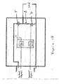
- Figure 1A shows a exploded view of a module according to the present invention.
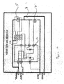
- Figure 1B a circuit schematic of a high side driver circuit as incorporated in a module according to the present invention.
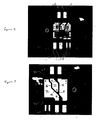
- Figure 2 shows a top plan view of a module according to the present invention having the lid thereof removed for viewing its internal elements.
- Figure 3 shows a bottom plan view of a module according to the present invention having the heatsink thereof removed.
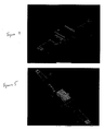
- Figure 4 is a first isometric view of a module according to the first embodiment of the present invention.
- Figure 5 is a second isometric view of a module according to the first embodiment of the present invention.
- Figure 6 is first isometric view of a module according to the second embodiment of the present invention.
- Figure 7 is a second isometric view of a module according to the second embodiment of the present invention.
- Figure 8 is a third isometric view of a module according to the second embodiment of the present invention.
- FIG. 9 illustrates a preferred use of a module according to the present invention.
- Figure 10 is a circuit schematic of a high side driver which is incorporated in a module according to the third embodiment of the present invention. schematically illustrates the arrangement of elements in a module according to the third embodiment.
- Figure 11 shows a top plan view of a module according to the third embodiment without a lid to shows the internal components thereof.
- Figure 12 shows a bottom plan view of a module according to third embodiment having the heatsink thereof, and portion of the shield thereof removed for illustration purposes.
- Figure 13 shows an isometric view of a module according to the third embodiment.
- Figure 14 shows a top plan view of a module according to the present invention.
- Figure 15 shows a bottom plan view of a module according to the present invention.
- Figure 16 shows a side plan view along line 16-16 viewed in the direction of the arrows shown in Figure 14.
- Figure 17 shows a front plant view along line 17-17 viewed in the direction of the arrows shown in Figure 14.
- a power module includes heatsink 1, thermally loaded adhesive body 2, molded shell 3, solder layers 4, reverse battery MOSFET 7, thermistor 6, high side driver MOSFET 5, free wheeling diode 8, small diameter wirebonds 9, large diameter wirebonds 10, adhesive layer 11, printed circuit board (PCB) assembly 12, encapsulating body 13, and lid 14.
- Figure 1B shows a circuit schematic of a high side driver circuit which is incorporated in a module according to the present invention.
- molded shell 3 includes a plurality of leads 20, 22, 24, 26, 28, 30, and a plurality of conductive pads 32, 34, 36.
- Leads 20, 30 are unitarily integrated with conductive pad 32 and extend through walls 40 of molded shell 40
- lead 28 is unitarily integrated with conductive pad 34 and extends through a wall 40 of molded shell 3
- lead 22 is unitarily integrated with conductive pad 36 and extends through an opposing wall 40 of molded shell 3.
- the phrase "unitarily integrated" as used herein means that the lead and the conductive pad are integrally connected to form a unitary body. To the integral connection between the leads and the conductive pads a portion of the heat generated by the semiconductor devices (discussed below) disposed on the conductive pads is dissipated through the leads.
- conductive pads 32, 34, 36 are spaced form one another. According to one aspect of the present invention the spaces between conductive pads 32, 34, 36 are filled with mold compound 38, which adheres to conductive pads 32, 34, 36. Thus, mold compound 38 resides in the spaces between conductive pads 32, 34, 36 and serves as electrical insulation as well as mechanical support for laterally supporting conductive pads 32, 34, 36 in place.
- molded shell 3 includes a plurality of walls 40 defining a space and formed on base portion 42, base portion 42 including spaced conductive pads 32, 34, 36 and mold compound 38.
- walls 40 are formed from the same material as mold compound 38 and integrated with the same to form a unitary molded shell having conductive pads 32,34,36 disposed at the bottom thereof.
- conductive pads 32, 34, 36 are exposed at the bottom of molded shell 3 at one side thereof, and receive at least one semiconductor element at an opposing side specifically.
- high side driver MOSFET 5 is electrically and mechanically attached to conductive pad 36 by a layer of solder 4
- free-wheeling diode 8 is electrically and mechanically attached to conductive pad 34 by a layer of solder 4
- reverse battery MOSFET 7 is electrically and mechanically attached to conductive pad 32 by a layer of solder 4.
- thermistor 6 is attached to conductive pad 32 by a layer of solder.
- a plurality of large diameter bondwires 10 connect the source electrode of high side MOSFET 5 to conductive pad 34, and a plurality of large diameter bondwires 10 connect the anode electrode of free-wheeling diode 8 to the source electrode of reverse battery MOSFET 7.
- PCB assembly 12 is disposed in the space defined by walls 40 and secured in place preferably by a layer of adhesive 11.
- PCB assembly has disposed thereon a respective IC driver package 42 for driving high side MOSFET 5 and reverse battery MOSFET 7.
- Each gate driver package 42 receives drive signals from an external controller through a respective lead 24, 26.
- each lead 24, 26 is electrically connected to a respective conductive pad 44 by a respective small diameter bondwire 9, and each conductive pad 44 may be electrically connected by any known manner to a respective gate driver 42, whereby control signals from leads 24, 26 may be transmitted to respective drivers 42.
- Each gate driver 42 is in turn, operatively connected to the gate electrode of a respective MOSFET 5, 7.
- small diameter bondwires 9 are used to connect a bondwire pad 46 to the gate electrode of a respective MOSFET 5, 7.
- Each bondwire pad 46 is in turn electrically connected by any known means (e.g. conductive traces) to a respective gate driver 42, whereby drive signals may be transmitted from a respective gate driver 42 to a respective MOSFET 5, 7.
- Thermistor 6 is also electrically connected to PCB assembly 12 in the same manner as the gate electrode of MOSFETs 5, 7 to provide temperature information as is known in the art.
- leads 20, 22 are power leads, leads 24, 26 are control leads, and leads 28, 30 are motor input and output leads.
- lead 22 is the power input lead B + from, for example, a battery
- lead 20 is the ground
- lead 28 provides power to a motor
- lead 30 is the motor's ground connection. That is, a motor's ground connection (or negative connection) is made through a lead provided in a module according to the present invention.
- encapsulating body 13 is disposed inside the space defined by walls 40 of molded shell 3. Furthermore, lid 14 is secured to walls 40 by an adhesive layer 11 to enclose the space defined by walls 40.
- a potting compound such as a silicone gel may be used for forming encapsulating body 13.
- wires 48 are soldered to leads 20, 22, 24, 26, 28, 30 and overmolded with a soft casing 50.
- a preferred material for forming soft casing 50 may be a soft-polyamide of the hot-melt variety which may overmold leads 20, 22, 24, 26, 28, 30 and at least the portion of wires 48 connected thereto.
- soft casing 50 renders strength to leads 20, 22, 24, 26, 28, 30 as well as their connection to wires 48, and protects the same from moisture and the like. Additionally, soft casing 50 adds aesthetic qualities to the modules by providing a "clean" exterior appearance.
- heatsink 1 is thermally connected to base 42 of molded shell 3.
- a thermally loaded adhesive layer 2 is interposed between heatsink 1 and base 42.
- the use of a thermally loaded adhesive in combination with heatsink 1 may eliminate the need for use of an expensive element such as an insulated metal substrate (IMS) or double-bonded copper (DBC), thereby reducing the cost of the module.
- IMS insulated metal substrate
- DRC double-bonded copper
- Thermally loaded adhesive layer 2 may be formed from any known elastomer compound, such as a silicone, which has thermally conductive particles such as Al 2 0 3 dispersed therein.
- the elastomer compound is selected to adhere heatsink 1 to base 42, aid in the transfer of heat from conductive pads 32, 34, 36 to heatsink 1, and electrically insulate heatsink 1 from conductive pads 32,34,36.
- snaps 52 may be provided on at least two opposing sides of molded shell 3. It should be noted that snaps 52 are adapted to engage the body of heatsink 1 in order to secure the same to molded shell 3.
- a module according to the second embodiment of the present invention does not include soft casing 50. Rather, a module according to the second embodiment of the present invention includes a shield 54 surrounding the leads.
- Each shield portion 54 is preferably formed from the same mold compound as that used for forming molded shell 3 and is preferably integral with the same.
- each shield 54 includes a connector portion 56 which is adapted to mate with a corresponding connector, e.g. a slot (not shown), on the shell of an electrical connector (not shown) having electrical connectors adapted for coupling with leads 20,22, 24,26,28,30.
- a module according to the present invention is preferably adapted for driving a brushless DC motor, such as fan motor used for engine cooling.
- a power module according to the present invention is a pass-through type module, which will be connected directly to the fan motor, and fastened to the fan shroud of the supplier of the fan assembly.
- molded shell 3 includes a molded bracket 58 which is integral with a wall 40 of molded shell 3. Bracket 58 preferably extends from a wall 40 that is disposed between leads 20,22,24,26,28,30.
- bracket 58 includes metal mounting insert 60 which is adapted to receive a fastener such as a screw to fasten molded shell 3 to a motor.
- a power module 59 according to the present invention can be mounted onto a motor 61 of a fan 62. Due to the opposing orientation of leads 20,22,24,26, and leads 28 and 30, power and control wires can be conveniently attached to one side of module 59, while wires designated for connection to motor 61 can be attached to the opposing side of module 59.
- a module according to the present invention allows for the shortest path for the wires, thereby reducing resistance and inductance contributed by the wires.
- a module 59 according to the present invention can be placed in the path of the fan air flow. As a result, smaller heatsinks can be used in a module 59 according to the present invention, thereby reducing the size of module 60 and its cost.
- a module according to the first embodiment and a module according to the second embodiment are suitable for driving a single fan motor.
- either embodiment may be connected in the following manner: Battery(+) to Power Input, Power Output to Fan Motor(+), Fan Motor (-) to Module, Module to Battery (-).
- a module according to the present invention can be used to drive two parallel connected fan motors.
- a module according to the third embodiment is placed in series on the positive bus.
- a module according to the third embodiment may be connected in the following manner: Battery(+) to Module, Module Output to Motor(+) (split into two outputs each going to a respective fan motor), Motor (-) to Battery (Motor (-) from both motors rejoin before connecting to the module).
- the battery connection in not made through the module, but is made outside the module.
- Figure 10 is a circuit schematic of a high side driver incorporated in a module according to the third embodiment of the present invention.
- a module according to the third embodiment extend through only one wall of molded shell 3.
- a module according to the third embodiment includes shield 54 surrounding leads 22,28,20,26.
- a module according to the third embodiment includes heatsink 1 which is in thermal communication with at least conductive pads 32,34,36 through a thermally conductive adhesive body 2 as seen in Figures 13-17.
- IC driver package 42 for driving the high side FET 5 is disposed on pad 36 alongside high side FET 3, and a driver circuit for driving reverse battery FET 7 is formed on circuit board 12.
- Circuit board 12 may be an IMS, DBC, an ordinary PCB or a thick film.
- a module according to the third embodiment is similar in construction to the first and second embodiments.
Landscapes
- Cooling Or The Like Of Semiconductors Or Solid State Devices (AREA)
- Inverter Devices (AREA)
Applications Claiming Priority (4)
| Application Number | Priority Date | Filing Date | Title |
|---|---|---|---|
| US49600003P | 2003-08-14 | 2003-08-14 | |
| US496000P | 2003-08-14 | ||
| US10/916,896 US7187551B2 (en) | 2003-08-14 | 2004-08-12 | Module for solid state relay for engine cooling fan control |
| US916896P | 2004-08-12 |
Publications (2)
| Publication Number | Publication Date |
|---|---|
| EP1507291A2 true EP1507291A2 (fr) | 2005-02-16 |
| EP1507291A3 EP1507291A3 (fr) | 2009-07-29 |
Family
ID=34381006
Family Applications (1)
| Application Number | Title | Priority Date | Filing Date |
|---|---|---|---|
| EP04019243A Withdrawn EP1507291A3 (fr) | 2003-08-14 | 2004-08-13 | Module de puissance pour relais à semi-conducteur |
Country Status (2)
| Country | Link |
|---|---|
| US (1) | US7187551B2 (fr) |
| EP (1) | EP1507291A3 (fr) |
Families Citing this family (37)
| Publication number | Priority date | Publication date | Assignee | Title |
|---|---|---|---|---|
| US7923827B2 (en) * | 2005-07-28 | 2011-04-12 | Infineon Technologies Ag | Semiconductor module for a switched-mode power supply and method for its assembly |
| DE102007018258A1 (de) * | 2007-04-13 | 2008-11-06 | Festo Ag & Co. Kg | Elektrische Linearantriebsvorrichtung |
| US8344556B2 (en) * | 2007-10-30 | 2013-01-01 | Sta-Rite Industries, Llc | Foam proportioning system with solid state contactor |
| US8807956B2 (en) | 2008-11-13 | 2014-08-19 | Marvell World Trade Ltd. | Apparatus and method for controlling speed of a fan via a first control module connected by a cable and/or conductors between a motor and a second control module |
| WO2012008713A2 (fr) * | 2010-07-15 | 2012-01-19 | 주식회사 제우스 | Relais statique |
| CN102447353B (zh) * | 2010-09-23 | 2016-03-02 | 马维尔国际贸易有限公司 | 风扇电动机控制系统 |
| CN102802375B (zh) * | 2011-05-24 | 2016-08-03 | 扬州海通电子科技有限公司 | 具有电源模组的电子装置 |
| KR20140006392A (ko) * | 2012-07-05 | 2014-01-16 | 엘에스산전 주식회사 | 자동차용 전장부품 박스 |
| US9560737B2 (en) * | 2015-03-04 | 2017-01-31 | International Business Machines Corporation | Electronic package with heat transfer element(s) |
| US10426037B2 (en) | 2015-07-15 | 2019-09-24 | International Business Machines Corporation | Circuitized structure with 3-dimensional configuration |
| US10175064B2 (en) | 2015-09-25 | 2019-01-08 | International Business Machines Corporation | Circuit boards and electronic packages with embedded tamper-respondent sensor |
| US10098235B2 (en) | 2015-09-25 | 2018-10-09 | International Business Machines Corporation | Tamper-respondent assemblies with region(s) of increased susceptibility to damage |
| US9578764B1 (en) | 2015-09-25 | 2017-02-21 | International Business Machines Corporation | Enclosure with inner tamper-respondent sensor(s) and physical security element(s) |
| US10172239B2 (en) | 2015-09-25 | 2019-01-01 | International Business Machines Corporation | Tamper-respondent sensors with formed flexible layer(s) |
| US9591776B1 (en) | 2015-09-25 | 2017-03-07 | International Business Machines Corporation | Enclosure with inner tamper-respondent sensor(s) |
| US9924591B2 (en) | 2015-09-25 | 2018-03-20 | International Business Machines Corporation | Tamper-respondent assemblies |
| US9911012B2 (en) | 2015-09-25 | 2018-03-06 | International Business Machines Corporation | Overlapping, discrete tamper-respondent sensors |
| US9894749B2 (en) | 2015-09-25 | 2018-02-13 | International Business Machines Corporation | Tamper-respondent assemblies with bond protection |
| US10143090B2 (en) | 2015-10-19 | 2018-11-27 | International Business Machines Corporation | Circuit layouts of tamper-respondent sensors |
| US9978231B2 (en) | 2015-10-21 | 2018-05-22 | International Business Machines Corporation | Tamper-respondent assembly with protective wrap(s) over tamper-respondent sensor(s) |
| US9913389B2 (en) | 2015-12-01 | 2018-03-06 | International Business Corporation Corporation | Tamper-respondent assembly with vent structure |
| US9555606B1 (en) | 2015-12-09 | 2017-01-31 | International Business Machines Corporation | Applying pressure to adhesive using CTE mismatch between components |
| US10327343B2 (en) | 2015-12-09 | 2019-06-18 | International Business Machines Corporation | Applying pressure to adhesive using CTE mismatch between components |
| US9554477B1 (en) | 2015-12-18 | 2017-01-24 | International Business Machines Corporation | Tamper-respondent assemblies with enclosure-to-board protection |
| US9916744B2 (en) | 2016-02-25 | 2018-03-13 | International Business Machines Corporation | Multi-layer stack with embedded tamper-detect protection |
| US9904811B2 (en) | 2016-04-27 | 2018-02-27 | International Business Machines Corporation | Tamper-proof electronic packages with two-phase dielectric fluid |
| US9913370B2 (en) | 2016-05-13 | 2018-03-06 | International Business Machines Corporation | Tamper-proof electronic packages formed with stressed glass |
| US9881880B2 (en) | 2016-05-13 | 2018-01-30 | International Business Machines Corporation | Tamper-proof electronic packages with stressed glass component substrate(s) |
| US9858776B1 (en) | 2016-06-28 | 2018-01-02 | International Business Machines Corporation | Tamper-respondent assembly with nonlinearity monitoring |
| US10321589B2 (en) | 2016-09-19 | 2019-06-11 | International Business Machines Corporation | Tamper-respondent assembly with sensor connection adapter |
| US10299372B2 (en) | 2016-09-26 | 2019-05-21 | International Business Machines Corporation | Vented tamper-respondent assemblies |
| US10271424B2 (en) | 2016-09-26 | 2019-04-23 | International Business Machines Corporation | Tamper-respondent assemblies with in situ vent structure(s) |
| US9999124B2 (en) | 2016-11-02 | 2018-06-12 | International Business Machines Corporation | Tamper-respondent assemblies with trace regions of increased susceptibility to breaking |
| US10327329B2 (en) | 2017-02-13 | 2019-06-18 | International Business Machines Corporation | Tamper-respondent assembly with flexible tamper-detect sensor(s) overlying in-situ-formed tamper-detect sensor |
| US10306753B1 (en) | 2018-02-22 | 2019-05-28 | International Business Machines Corporation | Enclosure-to-board interface with tamper-detect circuit(s) |
| US11122682B2 (en) | 2018-04-04 | 2021-09-14 | International Business Machines Corporation | Tamper-respondent sensors with liquid crystal polymer layers |
| CA3148674A1 (fr) * | 2021-02-14 | 2022-08-14 | Nominal Controls Inc. | Assemblage de contacteur a semiconducteurs de sortie de courant continu |
Family Cites Families (10)
| Publication number | Priority date | Publication date | Assignee | Title |
|---|---|---|---|---|
| DE4031051C2 (de) * | 1989-11-14 | 1997-05-07 | Siemens Ag | Modul mit mindestens einem Halbleiterschaltelement und einer Ansteuerschaltung |
| JP3168901B2 (ja) * | 1996-02-22 | 2001-05-21 | 株式会社日立製作所 | パワー半導体モジュール |
| US6132850A (en) * | 1996-11-25 | 2000-10-17 | Raytheon Company | Reworkable, thermally-conductive adhesives for electronic assemblies |
| DE19722355A1 (de) * | 1997-05-28 | 1998-12-03 | Bosch Gmbh Robert | Verfahren zur Herstellung elektrischer Baugruppen und elektrische Baugruppe |
| JPH11225459A (ja) * | 1998-02-05 | 1999-08-17 | Matsushita Electric Ind Co Ltd | モータ制御装置 |
| JPH11297906A (ja) * | 1998-03-23 | 1999-10-29 | Motorola Inc | 電子アセンブリおよび製造方法 |
| US6166464A (en) * | 1998-08-24 | 2000-12-26 | International Rectifier Corp. | Power module |
| US6212087B1 (en) * | 1999-02-05 | 2001-04-03 | International Rectifier Corp. | Electronic half bridge module |
| US6703703B2 (en) * | 2000-01-12 | 2004-03-09 | International Rectifier Corporation | Low cost power semiconductor module without substrate |
| US6912134B2 (en) * | 2000-09-12 | 2005-06-28 | International Rectifier Corporation | Fan control circuit and package |
-
2004
- 2004-08-12 US US10/916,896 patent/US7187551B2/en not_active Expired - Fee Related
- 2004-08-13 EP EP04019243A patent/EP1507291A3/fr not_active Withdrawn
Also Published As
| Publication number | Publication date |
|---|---|
| EP1507291A3 (fr) | 2009-07-29 |
| US7187551B2 (en) | 2007-03-06 |
| US20050068735A1 (en) | 2005-03-31 |
Similar Documents
| Publication | Publication Date | Title |
|---|---|---|
| US7187551B2 (en) | Module for solid state relay for engine cooling fan control | |
| US6441520B1 (en) | Power module | |
| EP1654761B1 (fr) | Module de puissance à semi-conducteurs | |
| US6307272B1 (en) | Semiconductor device and method for manufacturing the same | |
| TWI334216B (en) | Power semiconductor apparatus | |
| US8081472B2 (en) | Electric circuit device, electric circuit module, and power converter | |
| CN109952639B (zh) | 半导体装置、逆变器单元及汽车 | |
| CN112864113B (zh) | 功率器件、功率器件组件与相关装置 | |
| US11915999B2 (en) | Semiconductor device having a carrier, semiconductor chip packages mounted on the carrier and a cooling element | |
| JP7199167B2 (ja) | パワー半導体モジュール、電力変換装置、およびパワー半導体モジュールの製造方法 | |
| JP3780230B2 (ja) | 半導体モジュール及び電力変換装置 | |
| US6912134B2 (en) | Fan control circuit and package | |
| US6295201B1 (en) | Bus bar having embedded switching device | |
| CN100483704C (zh) | 用于epas/ehpas应用的模块 | |
| JP2002050722A (ja) | 半導体パッケージおよびその応用装置 | |
| US7019390B2 (en) | Silicon nitride insulating substrate for power semiconductor module | |
| WO2024203278A1 (fr) | Module à semi-conducteur et véhicule | |
| US11776940B2 (en) | Electronic power module | |
| JPH11220074A (ja) | 半導体装置 | |
| US20250014972A1 (en) | Package with clip directly connected to oblong electric connection element extending along mounting base | |
| JP2005327791A (ja) | 半導体装置およびその実装構造 | |
| JPH08204068A (ja) | モジュール構造の半導体装置 | |
| WO2026034269A1 (fr) | Module semi-conducteur, véhicule, et procédé de fabrication de module semi-conducteur | |
| WO2026034289A1 (fr) | Dispositif à semi-conducteur, module semi-conducteur et véhicule | |
| WO2026048612A1 (fr) | Dispositif à semi-conducteur, module semi-conducteur, véhicule et procédé de fabrication d'un dispositif à semi-conducteur |
Legal Events
| Date | Code | Title | Description |
|---|---|---|---|
| PUAI | Public reference made under article 153(3) epc to a published international application that has entered the european phase |
Free format text: ORIGINAL CODE: 0009012 |
|
| AK | Designated contracting states |
Kind code of ref document: A2 Designated state(s): AT BE BG CH CY CZ DE DK EE ES FI FR GB GR HU IE IT LI LU MC NL PL PT RO SE SI SK TR |
|
| AX | Request for extension of the european patent |
Extension state: AL HR LT LV MK |
|
| RAP1 | Party data changed (applicant data changed or rights of an application transferred) |
Owner name: SILICONIX TECHNOLOGY C.V. |
|
| PUAL | Search report despatched |
Free format text: ORIGINAL CODE: 0009013 |
|
| AK | Designated contracting states |
Kind code of ref document: A3 Designated state(s): AT BE BG CH CY CZ DE DK EE ES FI FR GB GR HU IE IT LI LU MC NL PL PT RO SE SI SK TR |
|
| AX | Request for extension of the european patent |
Extension state: AL HR LT LV MK |
|
| AKX | Designation fees paid | ||
| STAA | Information on the status of an ep patent application or granted ep patent |
Free format text: STATUS: THE APPLICATION IS DEEMED TO BE WITHDRAWN |
|
| 18D | Application deemed to be withdrawn |
Effective date: 20100130 |
|
| REG | Reference to a national code |
Ref country code: DE Ref legal event code: 8566 |