BACKGROUND OF THE INVENTION
1. Field of the Invention
The present invention relates to a method for implanting
ions into a semiconductor substrate and, more particularly, to a
method for implanting ions into a side wall of a protruded
semiconductor layer on a semiconductor substrate.
2. Description of the Related Art
In a production process for a large-scale semiconductor
integrated circuit employing a so-called planar technique, minute
semiconductor elements are formed in a plane on a surface of a
semiconductor substrate. For the formation of the semiconductor
elements, diffusion layers each serving as an N-conductivity region
or a P-conductivity region are generally formed in the
semiconductor substrate by utilizing an ion implantation
technique.
In the ion implantation technique, an impurity to be
implanted is ionized, and the resulting ions are accelerated by an
electric field and implanted into semiconductor crystals in the
semiconductor substrate. The implanted ions collide against
atoms and electrons in the semiconductor crystals and scatter in
the semiconductor crystals, thereby losing energy to stop after
traveling a predetermined distance in the semiconductor crystals.
Where the ions are implanted along a line normal to the surface of
the semiconductor substrate to selectively form a diffusion layer in
a portion of the semiconductor substrate exposed through a mask
opening, the implanted ions diffuse depthwise in the
semiconductor substrate with a certain ion concentration
distribution. The implanted ions also diffuse laterally in the
semiconductor substrate with a certain ion concentration
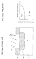
distribution. Fig. 9(a) is a sectional view of a P-type
semiconductor substrate 10 which has an N-type diffusion layer
20 formed therein, for example, by implanting phosphorus ions
into the semiconductor substrate 10 by applying a phosphorus ion
beam 70 through an opening provided in a resist 50 formed on the
substrate 10 by the ion implantation method. Fig. 9(b) is a
characteristic diagram illustrating an impurity concentration
distribution (the distribution of the concentration of the implanted
phosphorus ions) in a sectional plane A-A' in Fig. 9(a). As shown
in Fig. 9(b), the impurity concentration distribution is such that
the impurity concentration is the highest at the surface of the
semiconductor substrate and decreases depthwise apart from the
surface of the substrate. A region of the semiconductor substrate
having a higher impurity concentration is the N-type diffusion
region. In a semiconductor substrate region deeper than the
N-type diffusion region, an intrinsic impurity of the semiconductor
substrate is uniformly distributed.
In a so-called oblique ion implantation technique, ions are
implanted into a semiconductor substrate at a certain angle with
respect to a line normal to a surface of the semiconductor
substrate for expanding a lateral impurity distribution or for
preventing channeling. Fig. 10(a) is a sectional view of a P-type
semiconductor substrate 10 which has an N-type diffusion layer
20 formed therein, for example, by implanting phosphorus ions
into the semiconductor substrate 10 by applying a phosphorus ion
beam 70 at an angle with respect to a line normal to a surface of
the substrate 10 through an opening provided in a resist 50
formed on the substrate 10. Fig. 10(b) is a characteristic diagram
illustrating an impurity concentration distribution (the
distribution of the concentration of the implanted phosphorus
ions) in a sectional plane B-B' in Fig. 10(a). The depthwise
impurity concentration distribution in the plane B-B' is
substantially the same as in Fig. 9(b). The oblique ion
implantation technique makes it possible to implant the ions not
only perpendicularly to the surface of the semiconductor substrate
but also parallel to the surface of the semiconductor substrate.
Fig. 11 is a sectional view of a P-type semiconductor substrate 10
which has an N-type diffusion layer 20 formed in a surface portion
of the substrate and a side wall of a step of the substrate exposed
through an opening provided in a resist 50 formed on the
substrate 10. The formation of the diffusion layer 20 on the side
wall of the step is achieved, for example, by implanting
phosphorus ions into the semiconductor substrate 10 by applying
a phosphorus ion beam 70 at an angle with respect to a line
normal to the surface of the semiconductor substrate 10. The
oblique ion implantation method is employed, for example, for
forming an N-type MOS transistor of a gate overlap LDD structure
to minimize an overlap on a source side for microminiaturization
of a semiconductor device (see, for example, Japanese Unexamined
Patent Publication No. 05-114608 (1993)). Further, the oblique
ion implantation method is employed for introducing an impurity
into a trench side wall for highly accurately forming a device
isolation region in a self-aligning manner (see, for example,
Japanese Unexamined Patent Publication No. 2000-183154).
However, it is difficult to implant ions into a portion of the
semiconductor substrate perpendicular to the substrate surface by
the aforesaid oblique ion implantation. This is because it is
difficult to form a mask opening to expose only the portion of the
substrate perpendicular to the substrate surface by a
photolithography method employed in the so-called planar
technique in which circuit elements such as transistors are
formed in a plane on the semiconductor substrate.
In recent years, however, there is an increasing need for
micro-processing and higher density integration of circuit
elements. For example, nonvolatile memories typified by flash
EEPROMs have found extensive application as higher-capacity and
smaller-size information recording media for computers,
communication devices, measurement instruments, automated
control devices and personal daily life devices. Hence, there is an
increasing demand for less expensive and higher-capacity
nonvolatile memory cells. However, the size of such a memory
cell is determined by a minimum processing dimension (feature
size) which is defined by a resolution limit of the photolithography
technique. In order to achieve higher density integration without
relying on the improvement of the photolithography technique, a
three-dimensional memory cell arrangement technique has been
developed. In the three-dimensional memory cell arrangement
technique, the number of integrated memory cells is increased by
stacking the memory cells perpendicularly to the surface of the
semiconductor substrate for the higher density integration.
In order to stack circuit elements such as transistors of
the memory cells perpendicularly to the surface of the
semiconductor substrate by utilizing the three-dimensional
memory cell arrangement technique, there is a demand for an ion
implantation technique which permits highly accurate control of
ion implantation for implanting ions into a side wall of a
semiconductor substrate, i.e., in a direction parallel to the surface
of the semiconductor substrate.
SUMMARY OF THE INVENTION
In view of the foregoing, the present invention is directed
to an ion implantation technique which permits highly accurate
control of ion implantation for implanting ions in a direction
parallel to a surface of a semiconductor substrate.
According to the present invention, there is provided a
method for implanting ions into a side wall of a protruded
semiconductor layer on a semiconductor substrate, which
comprises applying an electric field to accelerate the ions in one
direction and applying a magnetic field parallel to a plane
extending at a predetermined angle with respect to the one
direction, thereby controlling a direction of the ion implantation to
the side wall.
Accelerating the ions in the one direction means that the
ions are put in the electric field applied toward the surface of the
semiconductor substrate thereby to be accelerated by Coulomb
force acting on the ions and projected toward the semiconductor
substrate. When the projected ions pass through the magnetic
field applied parallel to the plane extending at the predetermined
angle, Lorentz force acts on the ions, whereby the ions are
imparted with kinetic energy acting laterally of the direction of the
ion projection. As a result, the ions travel along a curved
trajectory thereby to be implanted into the side wall of the
protruded semiconductor layer.
According to the present invention, the ions accelerated in
the one direction by the application of the electric field are
subjected to the magnetic field applied parallel to the plane
extending at the predetermined angle with respect to the one
direction. Therefore, the direction of the ion implantation to the
side wall of the semiconductor substrate can be controlled with
high accuracy.
BRIEF DESCRIPTION OF THE DRAWINGS
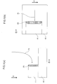
Figs. 1(a) and 1(b) are explanatory diagrams illustrating an
ion implantation method according to a first embodiment of the
present invention;
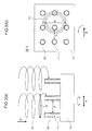
Figs. 2(a) and 2(b) are explanatory diagrams illustrating an
ion implantation method according to a second embodiment of the
present invention;
Figs. 3(a) and 3(b) are explanatory diagrams illustrating an
ion implantation method according to a third embodiment of the
present invention;
Figs. 4(a) and 4(b) are explanatory diagrams illustrating an
ion implantation method according to a fourth embodiment of the
present invention;
Figs. 5(a) and 5(b) are explanatory diagrams illustrating a
case where a magnetic field is rotated in an ion implantation
method according to a fifth embodiment of the present invention;
Figs. 6(a) and 6(b) are explanatory diagrams illustrating a
case where a substrate is rotated in the ion implantation method
according to the fifth embodiment of the present invention;
Figs. 7(a) and 7(b) are explanatory diagrams illustrating an
ion implantation method according to a sixth embodiment of the
present invention;
Figs. 8(a) and 8(b) are explanatory diagrams illustrating an
ion implantation method according to a seventh embodiment of
the present invention;
Figs. 9(a) and 9(b) are diagrams for explaining formation of
an N-type diffusion layer in a substrate surface by a conventional
ion implantation method;
Figs. 10(a) and 10(b) are diagrams for explaining formation
of an N-type diffusion layer in a substrate surface by a
conventional oblique ion implantation method; and
Fig. 11 is a diagram for explaining formation of an N-type
diffusion layer in a side wall of a step by the conventional oblique
ion implantation method.
DETAILED DESCRIPTION OF THE INVENTION
The present invention relates to a method for implanting
ions into a side wall of a protruded semiconductor layer on a
semiconductor substrate. According to the present invention, a
conventionally known semiconductor material such as silicon may
be employed as a material for the semiconductor substrate. A
step is formed on a surface of the semiconductor substrate by a
known method commonly employed in a three-dimensional
memory cell arrangement technique.
A known ion implantation apparatus for production of a
semiconductor device, for example, may be employed as an
apparatus for the ion implantation. In the known ion
implantation apparatus, an ion beam is generated and projected
by accelerating the ions put in the electric field. In one
embodiment of the present invention, the ions are projected at a
predetermined tilt angle with respect to the surface of the
semiconductor substrate. In another embodiment of the present
invention, the ions are projected perpendicularly to the surface of
the semiconductor substrate as in the conventional semiconductor
production method.
An inventive ion implantation method for implanting ions
into a side wall of a semiconductor layer comprises applying an
electric field to accelerate the ions in one direction and applying a
magnetic field parallel to a plane extending at a predetermined
angle with respect to the one direction. The magnetic field may
be rotated parallel to the plane extending at the predetermined
angle with respect to the electric field application direction, so that
the ions travel spirally in the electric field application direction.
Thus, the ions traveling spirally in the electric field application
direction are implanted into the side wall of the step not only in
the one direction but also in all the other directions.
The electric field may be applied perpendicularly to a
surface of the semiconductor substrate, and the magnetic field
may be applied parallel to the surface of the semiconductor
substrate.
The protruded semiconductor layer may include a plurality
of projection columns, and the magnetic field may be applied so
that the ions travel spirally with a diameter greater than a
distance between each two adjacent projection columns. Thus,
the ions traveling spirally with the diameter greater than the
distance between the adjacent projection columns are implanted
into the side wall of the step at a higher probability. Therefore,
the ion implantation to the side wall of the step can more
effectively be achieved.
Another inventive ion implantation method for implanting
ions into a side wall of a protruded semiconductor layer on a
semiconductor substrate, which comprises: forming an
implantation ion atmosphere on the vicinity of the protruded
semiconductor layer on the semiconductor substrate; and applying
an electric field parallel to a plane extending in parallel or at a
predetermined angle with respect to a surface of the
semiconductor substrate to accelerate the ions for the ion
implantation to the side wall of the semiconductor layer. Thus,
the implantation ion atmosphere is formed, and then the ions are
accelerated by the electric field and implanted into the side wall.
Therefore, the ion implantation to the side wall can be controlled
with high accuracy.
The electric field may be rotated parallel to the surface of
the semiconductor substrate. Thus, the ions are caused to travel
spirally by the rotation of the electric field for the ion implantation.
Therefore, the ions can be implanted into the side wall of the step
not only in one direction but also in all the other directions.
The protruded semiconductor layer may include a plurality
of projection columns.
The formation of the implantation ion atmosphere may be
provided by applying an electric field perpendicular to the
substrate surface so that the ions are transported to the vicinity of
the protruded semiconductor layer.
DESCRIPTION OF THE PREFERRED EMBODIMENTS
With reference to the attached drawings, the present
invention will hereinafter be described in detail by way of
embodiments thereof. However, it should be understood that the
invention be not limited to these embodiments.
First embodiment
Fig. 1(a) is a sectional view of a semiconductor substrate
for explaining an ion implantation method according to this
embodiment, and Fig. 1(b) is a plan view of the semiconductor
substrate as seen in the direction of projection of ions.
As shown in Figs. 1(a) and 1(b), a P-type silicon
semiconductor substrate 10 has a semiconductor layer 11
provided on a surface thereof. An ion beam 70 projected toward
the surface of the substrate 10 perpendicularly to the substrate
surface is accelerated by an electric field E applied in the same
direction as the ion beam projecting direction thereby to reach the
substrate 10. The ion beam 70 passes through a magnetic field B
applied parallel to the surface of the substrate 10. At this time,
Lorentz force acts on the ion beam 70, so that the ion beam 70 is
imparted with kinetic energy parallel to the silicon substrate
surface. As a result, the ion beam 70 travels along a curved
trajectory to reach the substrate 10, whereby the ions are
implanted into a side wall of the semiconductor layer 11 provided
on the surface of the substrate 10, i.e., into a side wall of a step of
the semiconductor layer 11. Thus, an N-type diffusion layer 20 is
formed in the side wall of the step.
The ions to be implanted are preferably phosphorus ions.
The dose of the ions to be implanted (the number of ions to be
implanted per unit area) is preferably 1×1010 cm-2 to 1×1016 cm-2,
and the kinetic energy to be imparted to the ions by the
application of the electric field E is preferably 1 keV to 5MeV.
The magnetic flux density of the magnetic field B to be applied is
preferably 1 µT to 100 T. However, the dose, the kinetic energy
and the magnetic flux density are not limited to the aforesaid
ranges.
In this embodiment, the N-type diffusion layer is formed in
the P-type semiconductor substrate, but a P-type diffusion layer
may be formed in an N-type semiconductor substrate in the
aforesaid manner. For the formation of the N-type diffusion layer
in the silicon substrate, arsenic ions or the like may be used
instead of the phosphorus ions. For the formation of the P-type
diffusion layer in the silicon substrate, boron ions or the like may
be used. The type of the ions to be implanted is not particularly
limited, as long as a desired diffusion layer can be provided. The
material for the semiconductor substrate is not limited to silicon.
Other exemplary materials for the semiconductor substrate
include a germanium semiconductor, a gallium-arsenic
semiconductor and an indium-phosphorus semiconductor.
When the ions are implanted into the side wall of the step,
it is desirable that the ions do not impinge on the surface of the
substrate 10 or a surface of the semiconductor layer 11 parallel to
the substrate surface. For prevention of the ion implantation to
the substrate surface or the semiconductor layer surface parallel
to the substrate surface, a hard mask such as a silicon oxide film
or a silicon nitride film is formed on the surface to be prevented
from the ion implantation. However, where the impingement of
the ions on the substrate surface or the semiconductor layer
surface parallel to the substrate surface causes no adverse effect,
there is no need to take the aforesaid measures.
The magnetic field B is preferably applied parallel to the
surface of the substrate 10 as described above, but the direction
of the application of the magnetic field B is not necessarily
required to be parallel to the substrate surface as long as the ions
can be implanted into the side wall of the step. Figs. 1(a) and
1(b) illustrate the case where the ions to be implanted have a
positive polarity. Where the ions to be implanted have a negative
polarity, the magnetic field B is applied in a direction opposite
from that shown in Fig. 1(b).
Second embodiment
In this embodiment, a magnetic field B applied parallel to
a surface of a P-type silicon semiconductor substrate 10 is rotated
in a plane parallel to the substrate surface. Thus, an ion beam
70 travels spirally with respect to the substrate surface to reach
the substrate surface. Fig. 2(a) is a sectional view of the
semiconductor substrate for explaining an ion implantation
method according to this embodiment, and Fig. 2(b) is a plan view
of the semiconductor substrate as seen in the direction of
projection of ions.
As shown in Figs. 2(a) and 2(b), the ion beam 70 is
projected toward the surface of the P-type silicon semiconductor
substrate 10 perpendicularly to the substrate surface, and
accelerated by an electric field E applied in the same direction as
the ion beam projecting direction thereby to reach the substrate
10. The ion beam 70 passes through the rotating magnetic field
B applied parallel to the surface of the substrate 10. At this time,
Lorentz force acts on the ion beam 70, so that the ion beam 70 is
imparted with kinetic energy parallel to the silicon substrate
surface. As a result, the ion beam 70 travels spirally to reach the
surface of the substrate 10, whereby the ions are implanted into a
side wall of a semiconductor layer 11 provided on the surface of
the substrate 10, i.e., into a side wall of a step of the
semiconductor layer 11. Thus, an N-type diffusion layer 20 is
formed in the side wall of the step.
The ions to be implanted are preferably phosphorus ions
or arsenic ions. The dose of the ions to be implanted is preferably
1×1010 cm-2 to 1×1016 cm-2, and the kinetic energy to be imparted
to the ions by the application of the electric field E is preferably 1
keV to 5MeV. The magnetic flux density of the magnetic field B to
be applied is preferably 1 µT to 100 T. The rotation speed of the
magnetic field B is preferably 1 rpm to 1000 rpm. However, the
lose, the kinetic energy, the magnetic flux density and the
rotation speed are not limited to the aforesaid ranges.
In this embodiment, the N-type diffusion layer is formed in
the P-type semiconductor substrate, but a P-type diffusion layer
may be formed in an N-type semiconductor substrate in the
aforesaid manner. For the formation of the N-type diffusion layer
n the silicon substrate, phosphorus ions or arsenic ions may be
used. For the formation of the P-type diffusion layer in the
silicon substrate, boron ions or the like may be used. The type of
the ions to be implanted is not particularly limited, as long as a
iesired diffusion layer can be provided. The material for the
semiconductor substrate is not limited to silicon. Other
exemplary materials for the semiconductor substrate include a
germanium semiconductor, a gallium-arsenic semiconductor and
an indium-phosphorus semiconductor.
When the ions are implanted into the side wall of the step,
it is desirable that the ions do not impinge on the surface of the
substrate 10 or a surface of the semiconductor layer 11 parallel to
the substrate surface. For prevention of the ion implantation to
the substrate surface or the semiconductor layer surface parallel
to the substrate surface, a hard mask such as a silicon oxide film
or a silicon nitride film is formed on the surface to be prevented
from the ion implantation. However, where the impingement of
the ions on the substrate surface or the semiconductor layer
surface parallel to the substrate surface causes no adverse effect,
there is no need to take the aforesaid measures.
The magnetic field B is preferably applied parallel to the
surface of the substrate 10 as described above, but the direction
of the application of the magnetic field B is not necessarily
required to be parallel to the substrate surface as long as the ions
can be implanted into the side wall of the step.
In this embodiment, the magnetic field B applied parallel
to the surface of the substrate 10 is rotated. Alternatively, the
substrate 10 but not the magnetic field B may be rotated. The
magnetic field B or the substrate 10 may be rotated either
clockwise or counterclockwise. Figs. 2(a) and 2(b) illustrate the
case where the ions to be implanted have a positive polarity.
However, this embodiment is also applicable to a case where the
ions to be implanted have a negative polarity.
Third embodiment
Figs. 3(a) and 3(b) illustrate a case where a semiconductor
layer 11 provided on a surface of a P-type silicon semiconductor
substrate 10 of a semiconductor device is shaped in a plurality of
projection columns thereby to have a plurality of steps. Fig. 3(a)
is a sectional view of the semiconductor substrate for explaining
an ion implantation method according to this embodiment, and Fig.
3(b) is a plan view of the semiconductor substrate as seen in the
direction of projection of ions.
In this embodiment, a magnetic field B is applied so that
an ion beam 70 travels spirally with a diameter D greater than a
distance d between each two adjacent projection columns as
shown in Fig. 7. If the magnetic field B is controlled so that the
diameter D and the distance d satisfy a relationship d<D, ions of
the ion beam 70 reaching the surface of the substrate 10 are
implanted into side walls of the projection columns of the
semiconductor layer 11 at a higher probability. Therefore, the ion
implantation to the side walls of the projection columns can
effectively be achieved.
The distance d between the adjacent projection columns of
the semiconductor layer 11 and the diameter D of the spiral
motion are preferably about 1 nm to about 10 µm, but are not
limited to this range.
In the plan views of Figs. 2(b) and 3(b), the diameter D of
the spiral motion of the ions increases toward the substrate 10,
but may decrease toward the substrate 10 or may be unchanged.
The change in the diameter D of the spiral motion of the ions
before the ions reach the silicon substrate after the projection of
the ions is not particularly limited, as long as the ion implantation
can be achieved as desired. Figs. 3(a) and 3(b) illustrate the case
where the ions to be implanted have a positive polarity. However,
this embodiment is also applicable to a case where the ions to be
implanted have a negative polarity.
Fourth embodiment
Fig. 4(a) is a sectional view of a semiconductor substrate
for explaining an ion implantation method according to this
embodiment. As shown in Fig. 4(a), a P-type silicon
semiconductor substrate 10 has a semiconductor layer 11
provided on a surface thereof and shaped in a plurality of
projection columns. Fig. 4(b) is a plan view of the semiconductor
substrate as seen from a side of the semiconductor substrate
formed with the semiconductor layer 11.
In this embodiment, an electric field E1 is applied
perpendicularly to the surface of the substrate 10 so as to cause
ions to travel to the vicinity of the surface of the substrate 10 for
ion transportation. Thus, an implantation ion atmosphere 75 is
formed in the vicinity of the substrate surface. Thereafter, an
electric field E2 is applied parallel to the substrate surface. Thus,
ions in the implantation ion atmosphere 75 are accelerated
parallel to the substrate surface. As a result, the ions are
implanted into side walls of the projection columns of the
semiconductor layer 11, whereby N-type diffusion layers 20 are
formed in the side walls of the projection columns.
The electric field E2 parallel to the substrate surface is
first applied for a predetermined period t1, and the application of
the electric field E2 is once stopped. Then, the electric field E 1
perpendicular to the substrate surface is applied to transport the
ions to the vicinity of the substrate surface. Alternatively, the
transportation of the ions to the vicinity of the silicon substrate
surface may be achieved by applying the electric field E1 while
applying the electric field E2.
The ions to be implanted are preferably phosphorus ions.
The dose of the ions to be implanted (the number of the ions to be
implanted per unit area) is preferably 1×1010 cm-2 to 1×1018 cm-2.
A kinetic energy to be imparted to the ions by the application of
the electric field E1 to transport the ions to the vicinity of the
substrate surface is preferably 1 keV to 5keV. A kinetic energy to
be imparted to the ions by the application of the electric field E2
parallel to the substrate surface is preferably 1 kV to 10MV.
However, the dose and the kinetic energies are not limited to the
aforesaid ranges.
In this embodiment, the N-type diffusion layer is formed in
the P-type semiconductor substrate, but a P-type diffusion layer
may be formed in an N-type semiconductor substrate in the
aforesaid manner. For the formation of the N-type diffusion layer
in the silicon substrate, arsenic ions or the like may be used
instead of the phosphorus ions. For the formation of the P-type
diffusion layer in the silicon substrate, boron ions or the like may
be used. The type of the ions to be implanted is not particularly
limited, as long as a desired diffusion layer can be provided. The
material for the semiconductor substrate is not limited to silicon.
Other exemplary materials for the semiconductor substrate
include a germanium semiconductor, a gallium-arsenic
semiconductor and an indium-phosphorus semiconductor.
The electric field E2 is desirably applied parallel to the
surface of the substrate 10 as described above, but the direction
of the application of the electric field E2 is not necessarily
required to be parallel to the substrate surface as long as the ions
can be implanted into the side walls of the steps.
Fifth embodiment
In this embodiment, an electric field E2 applied parallel to
a surface of a P-type silicon semiconductor substrate 10 is rotated
in a plane parallel to the substrate surface. Thus, ions travel
spirally with respect to the substrate surface to reach side walls of
projection columns of a semiconductor layer 11 provided on the
surface of the substrate 10. Fig. 5(a) is a sectional view of the
semiconductor substrate for explaining an ion implantation
method according to this embodiment, and Fig. 5(b) is a plan view
of the semiconductor substrate as seen from a side of the
semiconductor substrate formed with the semiconductor layer 11.
In this embodiment, an electric field E1 is applied
perpendicularly to the surface of the substrate 10 so as to cause
the ions to travel to the vicinity of the substrate surface for ion
transportation. Thus, an implantation ion atmosphere 75 is
formed in the vicinity of the substrate surface. Thereafter, the
electric field E2 is applied while being rotated in a plane parallel to
the substrate surface. Thus, the ions in the implantation ion
atmosphere 75 are accelerated parallel to the substrate surface.
As a result, the ions are implanted into the entire side walls of the
projection columns of the semiconductor layer 11, whereby N-type
diffusion layers 20 are formed in the side walls of the projection
columns.
The electric field E2 parallel to the substrate surface is
first applied for a predetermined period t1, and the application of
the electric field E2 is once stopped. Then, the electric field E1
perpendicular to the substrate surface is applied to transport the
ions to the vicinity of the substrate surface. Alternatively, the
transportation of the ions to the vicinity of the silicon substrate
surface may be achieved by applying the electric field E1 while
applying the electric field E2.
The ions to be implanted are preferably phosphorus ions.
The dose of the ions to be implanted (the number of the ions to be
implanted per unit area) is preferably 1×1010 cm-2 to 1×1018 cm-2.
A kinetic energy to be imparted to the ions by the application of
the electric field E1 to transport the ions to the vicinity of the
substrate surface is preferably 1 keV to 5keV. A kinetic energy to
be imparted to the ions by the application of the electric field E2
parallel to the substrate surface is preferably 1 kV to 10MV. The
rotation speed of the electric field E2 is preferably 1 rpm to 1000
rpm. However, the dose, the kinetic energies and the rotation
speed are not limited to the aforesaid ranges.
In this embodiment, the N-type diffusion layer is formed in
the P-type semiconductor substrate, but a P-type diffusion layer
may be formed in an N-type semiconductor substrate in the
aforesaid manner. For the formation of the N-type diffusion layer
in the silicon substrate, arsenic ions or the like may be used
instead of the phosphorus ions. For the formation of the P-type
diffusion layer in the silicon substrate, boron ions or the like may
be used. The type of the ions to be implanted is not particularly
limited, as long as a desired diffusion layer can be provided. The
material for the semiconductor substrate is not limited to silicon.
Other exemplary materials for the semiconductor substrate
include a germanium semiconductor, a gallium-arsenic
semiconductor and an indium-phosphorus semiconductor.
The electric field E2 is desirably applied parallel to the
surface of the substrate 10 as described above, but the direction
of the application of the electric field E2 is not necessarily
required to be parallel to the substrate surface as long as the ions
can be implanted into the side walls of the steps.
In this embodiment, the electric field E2 applied parallel to
the surface of the substrate 10 is rotated. In a modification of
this embodiment, the substrate 10 but not the electric field E2
may be rotated as shown in Fig. 6(a) which is a sectional view of
the semiconductor substrate subjected to ion implantation
according to the modification of the embodiment and Fig. 6(b)
which is a plan view of the semiconductor substrate as seen from
a side of the semiconductor substrate formed with the
semiconductor layer 11. The electric field E2 or the substrate 10
may be rotated either clockwise or counterclockwise.
Sixth embodiment
Fig. 7(a) is a sectional view of a semiconductor substrate
for explaining an ion implantation method according to this
embodiment, and Fig. 7(b) is a plan view of the semiconductor
substrate as seen from a side of the semiconductor substrate
formed with a semiconductor layer.
As shown in Figs. 7(a) and 7(b), an ion beam 71 is
projected at a predetermined tilt angle α with respect to a surface
of a P-type silicon semiconductor substrate 10. A magnetic field
B is applied perpendicularly to the surface of the semiconductor
substrate 10 from a source of the ion beam 71. The ion beam 71
projected in the magnetic field B is subjected to Lorentz force.
The Lorentz force acting on the ion beam 71 is directed parallel to
the substrate surface perpendicularly to the trajectory of the ion
beam 71. Therefore, the ion beam 71 travels spirally to reach the
substrate surface, whereby ions in the ion beam 71 are implanted
into a side wall of a semiconductor layer 11 provided on the
surface of the substrate 10, i.e., in a side wall of a step of the
semiconductor layer 11. Thus, an N-type diffusion layer 20 is
formed in the side wall of the step.
The ions to be implanted are preferably phosphorus ions
or arsenic ions. A kinetic energy to be imparted to the ions at the
projection of the ion beam 71 is preferably 1 keV to 5MeV, and the
dose of the ions to be implanted is preferably 1×1010 cm-2 to
1×1016 cm-2. The magnetic flux density of the magnetic field B to
be applied is preferably 1 µT to 100 T. However, the kinetic
energy, the dose and the magnetic flux density are not limited to
the aforesaid ranges.
In this embodiment, the N-type diffusion layer is formed in
the P-type semiconductor substrate, but a P-type diffusion layer
may be formed in an N-type semiconductor substrate in the
aforesaid manner. For the formation of the N-type diffusion layer
in the silicon substrate, phosphorus ions or arsenic ions may be
used. For the formation of the P-type diffusion layer in the
silicon substrate, boron ions or the like may be used. The type of
the ions to be implanted is not particularly limited, as long as a
desired diffusion layer can be provided. The material for the
semiconductor substrate is not limited to silicon. Other
exemplary materials for the semiconductor substrate include a
germanium semiconductor, a gallium-arsenic semiconductor and
an indium-phosphorus semiconductor.
When the ions are implanted into the side wall of the step,
it is desirable that the ions do not impinge on the surface of the
substrate 10 or a surface of the semiconductor layer 11 parallel to
the substrate surface. For prevention of the ion implantation to
the substrate surface or the semiconductor layer surface parallel
to the substrate surface, a hard mask such as a silicon oxide film
or a silicon nitride film is formed on the surface to be prevented
from the ion implantation. However, where the impingement of
the ions on the substrate surface or the semiconductor layer
surface parallel to the substrate surface causes no adverse effect,
there is no need to take the aforesaid measures.
The magnetic field B is preferably applied perpendicularly
to the surface of the substrate 10 as described above, but the
direction of the application of the magnetic field B is not
necessarily required to be perpendicular to the substrate surface
as long as the ions can be implanted into the side wall of the step.
Figs. 7(a) and 7(b) illustrate the case where the ions to be
implanted have a positive polarity. However, this embodiment is
also applicable to a case where the ions to be implanted have a
negative polarity.
Seventh embodiment
Figs. 8(a) and 8(b) illustrate a case where a semiconductor
layer 11 provided on a surface of a P-type silicon semiconductor
substrate 10 of a semiconductor device is shaped in a plurality of
projection columns thereby to have a plurality of steps. Fig. 8(a)
is a sectional view of the semiconductor substrate for explaining
an ion implantation method according to this embodiment, and Fig.
8(b) is a plan view of the semiconductor substrate as seen in the
direction of projection of ions.
In this embodiment, a magnetic field B is applied so that
an ion beam 71 travels spirally with a diameter D greater than a
distance d between each two adjacent projection columns. If the
magnetic field B is controlled so that the diameter D and the
distance d satisfy a relationship d<D, the ions in the ion beam 71
reaching the surface of the substrate 10 are implanted into side
walls of the projection columns of the semiconductor layer 11 at a
higher probability. Therefore, the ion implantation to the side
walls of the projection columns can effectively be achieved.
The distance d between the adjacent projection columns of
the semiconductor layer 11 and the diameter D of the spiral
motion are preferably about 1 nm to about 10 µm, but are not
limited to this range.
In the plan views of Figs. 7(b) and 8(b), the diameter D of
the spiral motion of the ions increases toward the substrate 10,
but may decrease toward the substrate 10 as shown in Fig. 8 or
may be unchanged. The change in the diameter D of the spiral
motion of the ions before the ions reach the silicon substrate after
the projection of the ions is not particularly limited, as long as the
ion implantation can be achieved as desired. Figs. 8(a) and 8(b)
illustrate the case where the ions to be implanted have a positive
polarity. However, this embodiment is also applicable to a case
where the ions to be implanted have a negative polarity.
According to the present invention, the electric field is
applied to accelerate the ions in the one direction, and the
magnetic field is applied parallel to the plane extending at the
predetermined angle with respect to the one direction. Therefore,
the ion implantation parallel to the surface of the semiconductor
substrate can be controlled with high accuracy.
The magnetic field may be rotated parallel to the plane
extending at the predetermined angle with respect to the direction
of the application of the electric field, so that the ions travel
spirally in the direction of the application of the electric field.
Thus, the ions traveling spirally in the direction of the application
of the electric field can be implanted into the side wall of the step
not only in the one direction but also in all the other directions.
Where the magnetic field is applied so that the ions travel
spirally with a diameter greater than a distance between every two
adjacent projection columns of the semiconductor layer, the ions
traveling spirally with the diameter greater than the distance
between the adjacent projection columns are implanted into the
side wall of the step at a higher probability. Thus, the ion
implantation to the side wall of the step can effectively be
achieved.
Where the electric field is applied parallel to the plane
extending at the predetermined angle with respect to the substrate
surface after the implantation ion atmosphere is formed on the
protruded semiconductor layer on the semiconductor substrate,
the ions in the implantation ion atmosphere are accelerated by the
electric field thereby to be implanted into the side wall. Therefore,
the ion implantation to the side wall can be controlled with high
accuracy.
Where the electric field is rotated parallel to the surface of
the semiconductor substrate, the ions are caused to travel spirally
by the application of the electric field for the ion implantation.
Therefore, the ions can be implanted into the side wall of the step
not only in the one direction but also in all the other directions.