EP1505691A2 - Steerable leaky wave antenna capable of both forward and backward radiation - Google Patents
Steerable leaky wave antenna capable of both forward and backward radiation Download PDFInfo
- Publication number
- EP1505691A2 EP1505691A2 EP04010832A EP04010832A EP1505691A2 EP 1505691 A2 EP1505691 A2 EP 1505691A2 EP 04010832 A EP04010832 A EP 04010832A EP 04010832 A EP04010832 A EP 04010832A EP 1505691 A2 EP1505691 A2 EP 1505691A2
- Authority
- EP
- European Patent Office
- Prior art keywords
- antenna
- impedance
- tunable
- tunable impedance
- patches
- Prior art date
- Legal status (The legal status is an assumption and is not a legal conclusion. Google has not performed a legal analysis and makes no representation as to the accuracy of the status listed.)
- Ceased
Links
- 230000005855 radiation Effects 0.000 title claims description 26
- 238000000034 method Methods 0.000 claims abstract description 39
- 239000003990 capacitor Substances 0.000 claims description 14
- 230000000737 periodic effect Effects 0.000 claims description 11
- 239000000758 substrate Substances 0.000 claims description 11
- 125000004122 cyclic group Chemical group 0.000 claims 3
- 238000012804 iterative process Methods 0.000 claims 3
- 238000005516 engineering process Methods 0.000 description 14
- 239000013598 vector Substances 0.000 description 9
- 239000002184 metal Substances 0.000 description 6
- 229910052751 metal Inorganic materials 0.000 description 6
- 230000003044 adaptive effect Effects 0.000 description 4
- 238000010586 diagram Methods 0.000 description 3
- 239000006185 dispersion Substances 0.000 description 3
- 230000001902 propagating effect Effects 0.000 description 3
- 238000013459 approach Methods 0.000 description 2
- 238000013461 design Methods 0.000 description 2
- 230000005684 electric field Effects 0.000 description 2
- 239000000463 material Substances 0.000 description 2
- 238000005259 measurement Methods 0.000 description 2
- 230000008569 process Effects 0.000 description 2
- RYGMFSIKBFXOCR-UHFFFAOYSA-N Copper Chemical compound [Cu] RYGMFSIKBFXOCR-UHFFFAOYSA-N 0.000 description 1
- 229910000881 Cu alloy Inorganic materials 0.000 description 1
- 238000004458 analytical method Methods 0.000 description 1
- 230000008859 change Effects 0.000 description 1
- 238000004891 communication Methods 0.000 description 1
- 239000004020 conductor Substances 0.000 description 1
- 229910052802 copper Inorganic materials 0.000 description 1
- 239000010949 copper Substances 0.000 description 1
- 230000001351 cycling effect Effects 0.000 description 1
- 230000003247 decreasing effect Effects 0.000 description 1
- 230000005284 excitation Effects 0.000 description 1
- 238000002474 experimental method Methods 0.000 description 1
- 230000003993 interaction Effects 0.000 description 1
- 239000004973 liquid crystal related substance Substances 0.000 description 1
- 150000002739 metals Chemical class 0.000 description 1
- 238000012986 modification Methods 0.000 description 1
- 230000004048 modification Effects 0.000 description 1
- 230000009467 reduction Effects 0.000 description 1
- 239000004065 semiconductor Substances 0.000 description 1
- 239000007787 solid Substances 0.000 description 1
- 238000012360 testing method Methods 0.000 description 1
Images



Classifications
-
- H—ELECTRICITY
- H01—ELECTRIC ELEMENTS
- H01Q—ANTENNAS, i.e. RADIO AERIALS
- H01Q9/00—Electrically-short antennas having dimensions not more than twice the operating wavelength and consisting of conductive active radiating elements
- H01Q9/04—Resonant antennas
- H01Q9/0407—Substantially flat resonant element parallel to ground plane, e.g. patch antenna
- H01Q9/0442—Substantially flat resonant element parallel to ground plane, e.g. patch antenna with particular tuning means
-
- H—ELECTRICITY
- H01—ELECTRIC ELEMENTS
- H01Q—ANTENNAS, i.e. RADIO AERIALS
- H01Q13/00—Waveguide horns or mouths; Slot antennas; Leaky-waveguide antennas; Equivalent structures causing radiation along the transmission path of a guided wave
- H01Q13/20—Non-resonant leaky-waveguide or transmission-line antennas; Equivalent structures causing radiation along the transmission path of a guided wave
-
- H—ELECTRICITY
- H01—ELECTRIC ELEMENTS
- H01Q—ANTENNAS, i.e. RADIO AERIALS
- H01Q15/00—Devices for reflection, refraction, diffraction or polarisation of waves radiated from an antenna, e.g. quasi-optical devices
- H01Q15/0006—Devices acting selectively as reflecting surface, as diffracting or as refracting device, e.g. frequency filtering or angular spatial filtering devices
- H01Q15/0013—Devices acting selectively as reflecting surface, as diffracting or as refracting device, e.g. frequency filtering or angular spatial filtering devices said selective devices working as frequency-selective reflecting surfaces, e.g. FSS, dichroic plates, surfaces being partly transmissive and reflective
- H01Q15/002—Devices acting selectively as reflecting surface, as diffracting or as refracting device, e.g. frequency filtering or angular spatial filtering devices said selective devices working as frequency-selective reflecting surfaces, e.g. FSS, dichroic plates, surfaces being partly transmissive and reflective said selective devices being reconfigurable or tunable, e.g. using switches or diodes
-
- H—ELECTRICITY
- H01—ELECTRIC ELEMENTS
- H01Q—ANTENNAS, i.e. RADIO AERIALS
- H01Q19/00—Combinations of primary active antenna elements and units with secondary devices, e.g. with quasi-optical devices, for giving the antenna a desired directional characteristic
- H01Q19/28—Combinations of primary active antenna elements and units with secondary devices, e.g. with quasi-optical devices, for giving the antenna a desired directional characteristic using a secondary device in the form of two or more substantially straight conductive elements
- H01Q19/32—Combinations of primary active antenna elements and units with secondary devices, e.g. with quasi-optical devices, for giving the antenna a desired directional characteristic using a secondary device in the form of two or more substantially straight conductive elements the primary active element being end-fed and elongated
-
- H—ELECTRICITY
- H01—ELECTRIC ELEMENTS
- H01Q—ANTENNAS, i.e. RADIO AERIALS
- H01Q21/00—Antenna arrays or systems
- H01Q21/06—Arrays of individually energised antenna units similarly polarised and spaced apart
- H01Q21/061—Two dimensional planar arrays
-
- H—ELECTRICITY
- H01—ELECTRIC ELEMENTS
- H01Q—ANTENNAS, i.e. RADIO AERIALS
- H01Q23/00—Antennas with active circuits or circuit elements integrated within them or attached to them
-
- H—ELECTRICITY
- H01—ELECTRIC ELEMENTS
- H01Q—ANTENNAS, i.e. RADIO AERIALS
- H01Q3/00—Arrangements for changing or varying the orientation or the shape of the directional pattern of the waves radiated from an antenna or antenna system
- H01Q3/44—Arrangements for changing or varying the orientation or the shape of the directional pattern of the waves radiated from an antenna or antenna system varying the electric or magnetic characteristics of reflecting, refracting, or diffracting devices associated with the radiating element
- H01Q3/443—Arrangements for changing or varying the orientation or the shape of the directional pattern of the waves radiated from an antenna or antenna system varying the electric or magnetic characteristics of reflecting, refracting, or diffracting devices associated with the radiating element varying the phase velocity along a leaky transmission line
-
- H—ELECTRICITY
- H01—ELECTRIC ELEMENTS
- H01Q—ANTENNAS, i.e. RADIO AERIALS
- H01Q3/00—Arrangements for changing or varying the orientation or the shape of the directional pattern of the waves radiated from an antenna or antenna system
- H01Q3/44—Arrangements for changing or varying the orientation or the shape of the directional pattern of the waves radiated from an antenna or antenna system varying the electric or magnetic characteristics of reflecting, refracting, or diffracting devices associated with the radiating element
- H01Q3/46—Active lenses or reflecting arrays
Definitions
- This disclosure describes a low-cost, electronically steerable leaky wave antenna. It involves several parts: (1) An electronically tunable impedance surface, (2) a low-profile antenna mounted adjacent to that surface, and (3) a means of tuning the surface to steer the radiated beam in the forward and backward direction, and to improve the gain relative to alternative leaky wave techniques.
- the presently disclosed technology relates to an electronically steerable leaky wave antenna that is capable of steering in both the forward and backward direction. It is based on a tunable impedance surface, which has been described in previous patent applications, including the application that matured into U.S. Patent no. 6,496,155 listed above. It is also based on a steerable leaky wave antenna, which has been described in previous patent applications, including the application that matured into U.S. Patent no. 6,496,155 listed above. However, in the previous disclosures, it was not disclosed how to produce backward leaky wave radiation, and therefore the steering range of the antenna was limited. Furthermore, the presently described technology also provides new ways of improving the gain of leaky wave antennas.
- a tunable impedance surface is shown in Figures 1(a) and 1(b) at numeral 10. It includes a lattice of small metal patches 12 printed on one side of a dielectric substrate 11, and a ground plane 16 printed on the other side of the dielectric substrate 11. Some (typically one-half) of the patches 12 are connected to the ground plane 16 through metal plated vias 14, while the remaining patches are connected by vias 18 to bias lines 18' that are located on the other side of the ground plane 16, which vias 18 penetrate the ground plane 16 through apertures 22 therein.
- the patches 12 are each connected to their neighbors by varactor diodes 20.
- the biased patches are easily identifiable since they are each associated with a metal plated vias 14 that penetrate the integral ground plane 16 through openings 22 in the ground plane, the openings 22 being indicated by dashed lines in Figure 1 (a).
- the ground patches are those that have no associated opening 22.
- the diodes 20 are arranged so that when a positive voltage is applied to the biased patches, the diodes 20 reverse-biased.
- the return path that completes the circuit consists of the grounded patches that are coupled to the ground plane 16 by vias 14.
- the biased and grounded patches 12 are preferably arranged in a checkerboard pattern. While this technology preferably uses this particular embodiment of a tunable impedance surface as the preferred embodiment, other ways of making a tunable impedance surface can also be used. Specifically, any lattice of coupled and tunable oscillators could be used.
- this surface is used as an electronically steerable reflector, but that is not the subject of the present disclosure.
- the surface is used as a tunable substrate that supports leaky waves, which is the mode that is employed for this technology.
- This tuning technique has been the subject of other patent applications with both mechanically tuned and electrically tuned structures using a method referred to here as the "traditional method.”
- leaky waves are launched across the tunable surface 10 using a flared notch antenna 30, such as shown in Figure 2.
- the flared notch antenna 30 excites a transverse electric (TE) wave 32, which travels across the surface.
- TE waves are leaky, which means that they radiate a portion of their energy 34 as they travel across the tunable surface 10.
- the angle at which the leaky waves radiate can be steered.
- All of the varactor diodes 20 are provided with the same bias voltage, so that the resonance frequency of each unit cell (a unit cell is defined by as a single patch 12 with one-half of each connected varactor diode 20 or equivalently as a single varactor diode 20 with one-half of each connected patch 12) changes by the same amount, and the surface impedance properties are uniform across the surface 10.
- the traditional leaky wave beam steering method can be understood by examining the dispersion diagram shown in Figure 3.
- the textured, tunable impedance surface 10 supports both TM and TE waves at different frequencies. TM waves are supported below the resonance frequency, denoted by ⁇ 1 , and TE waves are supported above it.
- the "light line,” denoted by the diagonal line, represents electromagnetic waves moving in free space. All modes that lie below the light line are bound to the surface, and cannot radiate.
- the wave vector along the tunable impedance surface must match the tangential component of the radiated wave.
- the radiated beam can be steered in the elevation plane by tuning the resonance frequency from ⁇ 1 to ⁇ 2 .
- the surface resonance frequency is ⁇ 1 , indicated by the solid line in Figure 3
- a wave launched across the surface at ⁇ A will have wave vector k 1 .
- the wave vector changes to k 2 , and the radiated beam is steered to a different angle.
- the beam angle q varies from near the horizon to near zenith as the resonance frequency is increased. In this traditional beam steering method, the entire surface is tuned uniformly.
- the radiated beam 32 can be steered over a range of roughly 5 degrees to 40 degrees from zenith, as shown in Figures 5(a) - 5(e).
- Figures (a) - 5(e) present graphs of measured results using the traditional leaky wave beam steering method with a uniform surface impedance obtained by applying the indicated DC voltages uniformly to all varactor diodes 20 in the electrically tunable surface 10. Radiation directly toward zenith or close to the horizon is not practical, and backward leaky wave radiation is not possible. Measurements were taken at 4.5 GHz for Figures 5(a) - 5(e) with patch sizes of 0.9 cm disposed on 1.0 cm centers.
- the substrate 11 had a dielectric constant of 2.2, and was 62 mils (1.6 mm) thick.
- the varactor diodes 20 had an effective tuning range of 0.2 to 0.8 pF.
- presently described technology relates to a new technology for leaky wave beam steering that is capable of steering in a backward direction, as well as further down toward the horizon in the forward direction than was previously possible, and also directly toward zenith.
- the disclosed antenna and method involve applying a non-uniform voltage function across the tunable impedance surface. If the voltage function is periodic or nearly periodic, this can be understood as a super-lattice of surface impedances that produces a folding the surface wave band structure in upon itself, creating a band having group velocity and phase velocity in opposite directions.
- An antenna placed near the surface couples into this backward band, launching a leaky wave that propagates in the forward direction, but radiates in the backward direction. From another point of view, the forward-running leaky wave is scattered backward by the periodic surface impedance, resulting in backward radiation.
- the presently described technology provides an antenna having: a tunable impedance surface: an antenna disposed on said tunable impedance surface, said antenna having a conventional forward direction of propagation when disposed on said tunable impedance surface while said surface has an uniform impedance pattern; and some means for adjusting the impedance of pattern of the tunable impedance surface along the normal direction for propagation so that the impedance pattern assumes a cyclical pattern along the normal pattern of propagation.
- the new beam steering technology disclosed herein can be summarized, in one aspect, by the following statement:
- the impedance of the tunable impedance surface 10 is tuned in a non-uniform manner to create an impedance function across the surface, so that when a wave 32 is launched across the surface, it is scattered by this impedance function to a desired radiation angle.
- impedance function is periodic or nearly periodic. This can be thought of as being equivalent to a microwave grating, where the surface waves are scattered by the grating into a direction that is determined by phase matching on the surface.
- the radiation angle is determined by the difference between the wave vector along the surface, and the wave vector that describes the periodic impedance function, as shown in Figure 6.
- the band structure of the tunable impedance surface 10 is folded in upon itself, because the period of the surface has been increased to that of the periodic impedance function, as shown in Figure 7(a).
- This folding of the band structure results in a backward propagating band, in which the phase velocity and group velocity of the surface waves are in opposite directions. Then, when a leaky wave propagates in the forward direction, it leaks in the backward direction, because the radiation angle is determined by phase matching at the surface.
- the TM band is not folded because it still sees a uniform surface.
- FIGs 7(b) and 7(c) diagrammatically depict an experiment that was performed using an electrically tunable surface 10.
- the solid dots in the center of the patches 12 are grounded vias 14, while the open dots reflect biased vias 18. Alternate columns of patches 12 were biased at two different voltages, which one may call simply high and low.
- the relatively high voltages are shown as grey regions between two patches 12, while the relatively low voltages are shown as white regions between two patches 12.
- k Assume a wave is traveling in the direction designated as k, with an electric field polarized in the direction shown by the letter E.
- variable capacitor elements 20 can take a variety of forms, including microelectromechanical system (MEMS) capacitors, plunger-type actuators, thermally activated bimetallic plates, or any other device for effectively varying the capacitance between a pair of capacitor plates.
- MEMS microelectromechanical system
- the variable capacitors 20 can alternatively be solid-state devices, in which a ferroelectric or semiconductor material provides a variable capacitance controlled by an externally applied voltage, such as the varactor diodes mentioned above.
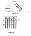
- Figure 7(d) shows a testing setup including a receiver horn 42 directed towards a tunable surface 10 which is disposed at the angle ⁇ with reference to a line perpendicular to surface 10 (which means that the tunable surface 10 is disposed at the angle 90- ⁇ with reference to center axis A of horn 42).
- the patches 12 on the surface 10 are arranged in columns, such as columns 1 - n identified in Figure 7(e).
- a voltage v is applied to each column and that voltage can be increased or decreased by a voltage ⁇ .
- the voltages applied to the columns 1 - n can be v- ⁇ , v or v+ ⁇ .
- the tunable surface 10 has an antenna disposed thereon such as the flared notch antenna 30 depicted in Figure 2.
- a signal is applied to the antenna and the power of the signal received at horn 42 is measured for each case of v- ⁇ , v and v+ ⁇ .
- the best of the three cases is selected for column n and the process is repeated for column n+1, cycling through all columns of patches.
- the selected voltage values cease to change significantly from one cycle to the next, then the value of ⁇ is reduced and the process is repeated until the fluctuations in the received power are negligible.
- This technique takes about fifty cycles through the n columns to converge a good solution of the appropriate values of the bias voltages for the columns of controlled patches for the angle ⁇ .
- This sort of technique to find best values of the bias voltages is somewhat of a brute force technique and better techniques may be known to those skilled in the art of converging iterative solutions.
- the size of the radiating regions can also be controlled so that the decay of the wave is balanced by greater radiation from regions that are further from the source. See Figure 8(c).
- this model as well as the band structure folding model or any other model, is an over-simplification of a complex interaction between the wave and the surface, but it is one way to understand the behavior of the tunable impedance surface 10 and to enable antennas using such a surface to be designed.
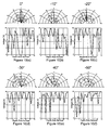
- Figures 9(a) - 9(e) show beam steering in the forward direction, for different positive angles, and also the voltages applied to the columns of patches 12 as previously explained with reference to Figures 7(d) and 7(e).
- Figures 10(a) - 10(f) show beam steering to zero and negative angles, for various non-positive angles, and also the voltage applied to the columns of controlled patches 12.
- the voltage function is also displayed. The voltages were obtained by applying an adaptive (iterative) algorithm to the surface that maximized the radiated power in the desired direction.
- the periodicity of voltages can clearly be seen.
- the shortest period is for the -50 degree case, where the forward propagating surface wave must be scattered into the opposite direction.
- About six periods can be distinguished in the voltage function for this case.
- For the zero degree case see Figure 10(a)
- about four periods can be distinguished, while for the +50 degree case (see Figure 9(e)), only about one period is found.
- the applied voltages control the impedance function of the electrically tunable surface 10.
- the use of a non-uniform surface impedance can provide several advantages.
- the beam can be steered in both the forward and backward direction, and can be steered over a greater range in the forward direction for the case of the non-uniform applied voltage.
- this can be understood by examining the periodicity of the voltage function that was obtained by the adaptive algorithm that optimized the radiated power in the desired direction.
- the measured data can be fit to this formula in order to obtain the effective index as seen by the surface wave. Based on experimental data, the effective index has been found to be about 1.2. One might expect that the wave sees an average of the index of refraction of the substrate used to construct the surface (1.5), and that of air (1.0), so the observed effective index is reasonable.
- the non-uniform surface also produces higher gain and narrower beam width for the cases of the non-uniform applied voltage.
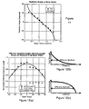
- the effective aperture size can be estimated from the 3 dB beamwidth of the radiation pattern, as shown in Figure 12(a).
- the case of uniform voltage has nearly constant effective aperture length, as one might expect.
- the surface wave interacts more closely with the tunable impedance surface 10, thus extending the effective aperture.
- the effective aperture of a large antenna should have a cosine dependence, because it appears smaller at sharper angles.
- the effective surface length follows this expected dependence, and it uses nearly the entire length of the surface.
- Figures 12(b) and 12(c) are graphs of the effective aperture distance versus field strength and demonstrate that by using a non-uniform surface impedance function, the effective aperture length is nearly the entire length of the surface (see Figure 12(c), while a much smaller size is obtained for the uniform impedance function case (see Figure 12(b)).
- the tunable impedance surface 10 that is preferably used is the tunable impedance surface discussed above with reference to Figure 2.
- the patches 12 need not be square. Other shapes could be used instead, including circularly or hexagonal shaped patches 12 (see, for example, my U.S. Patent No. 6,538,621 issued Match 25, 2003).
- other techniques than the use of varactor diodes 20 can be utilized to adjust the impedance of the surface 10. For example, in my U.S. Patent 6,552,696 issued April 22, 2003 wherein I teach how to adjust the impedance of a tunable impedance surface of the type having patches 12 using liquid crystal materials and indicated above, other types of variable capacitor elements may be used instead.
- the tunable impedance surface 10 is depicted as being planar.
- the presently described technology is not limited to planar tunable impedance surfaces.
- the printed circuit board technology preferably used to provide a substrate 11 for the tunable impedance surface 10 can provide a very flexible substrate 11.
- the tunable impedance surface 10 can be mounted on most any convenient surface and conform to the shape of that surface. The tuning of the impedance function would then be adjusted to account for the shape of that surface.
- surface 10 can be planar, non-planar, convex, concave or have most any other shape by appropriately tuning its surface impedance.
- the top plate elements 12 and the ground or back plane element 16 are preferably formed from a metal such as copper or a copper alloy conveniently used in printed circuit board technologies. However, non-metallic, conductive materials may be used instead of metals for the top plate elements 12 and/or the ground or back plane element 16, if desired.
Landscapes
- Variable-Direction Aerials And Aerial Arrays (AREA)
- Waveguide Aerials (AREA)
Abstract
Description
- This disclosure describes a low-cost, electronically steerable leaky wave antenna. It involves several parts: (1) An electronically tunable impedance surface, (2) a low-profile antenna mounted adjacent to that surface, and (3) a means of tuning the surface to steer the radiated beam in the forward and backward direction, and to improve the gain relative to alternative leaky wave techniques.
- The prior art includes:
- 1. Daniel Sievenpiper, US Patent No. 6,496,155
- 2. P. W. Chen, C. S. Lee, V. Nalbandian, "Planar Double-Layer Leaky Wave Microstrip Antenna", IEEE Transactions on Antennas and Propagation, vol. 50, pp. 832-835, 2002
- 3. C.-J. Wang, H. L. Guan, C. F. Jou, "Two-dimensional scanning leaky-wave antenna by utilizing the phased array", IEEE Microwave and Wireless Components Letters, vol. 12, no. 8 , pp. 311-313, 2002
- 4. J. Sor, C.-C. Chang, Y. Qian, T. Itoh, "A reconfigurable leaky-wave/patch microstrip aperture for phased-array applications", IEEE Transactions on Microwave Theory and Techniques, vol. 50, no. 8, pp. 1877-1884, 2002
- 5. C.-N. Hu, C.-K.C. Tzuang, "Analysis and design of large leaky-mode array
employing the coupled-mode approach", IEEE Transactions on Microwave
Theory and Techniques, vol. 49 no. 4,
part 1, pp. 629-636, 2001 - 6. E. Semouchkina, W. Cao, R. Mittra, G. Semouchkin, N. Popenko, I. Ivanchenko, "Numerical modeling and experimental study of a novel leaky wave antenna", Antennas and Propagation Society 2001 IEEE International Symposium, vol. 4, pp. 234-237,2001
- 7. J. W. Lee, J. J. Eom, K. H. Park, W. J. Chun, "TM-wave radiation from grooves in a dielectric-covered ground plane", IEEE Transactions on Antennas and Propagation, vol. 49, no. 1, pp. 104-105, 2001
- 8. Y. Yashchyshyn, J. Modelski, "The leaky-wave antenna with ferroelectric substrate", 14th International Conference on Microwaves, Radar and Wireless Communications, MIKON-2002, vol. 1, pp. 218 -221, 2002
- 9. H.-Y.D. Yang, D. R. Jackson, "Theory of line-source radiation from a metal-strip grating dielectric-slab structure", IEEE Transactions on Antennas and Propagation, vol. 48, no. 4, pp. 556 -564, 2000
- 10. A. Grbic, G. V. Eleftheriades, "Experimental verification of backward wave radiation from a negative refractive index metamaterial", Journal of Applied Physics, vol. 92, no. 10
- 11. J. W. Sheen, "Wideband microstrip leaky wave antenna and its feeding system", US patent 6404390B2
- 12. T. Teshirogi, A. Yamamoto, "Planar antenna and method for manufacturing same", US patent 6317095B1
- 13. V. Nalbandian, C. S. Lee, "Compact Wideband Microstrip Antenna with Leaky Wave Excitation", US patent 6285325
- 14. R. J. King, "Non-uniform variable guided wave antennas with electronically controllable scanning", US Patent 4150382
-
- The presently disclosed technology relates to an electronically steerable leaky wave antenna that is capable of steering in both the forward and backward direction. It is based on a tunable impedance surface, which has been described in previous patent applications, including the application that matured into U.S. Patent no. 6,496,155 listed above. It is also based on a steerable leaky wave antenna, which has been described in previous patent applications, including the application that matured into U.S. Patent no. 6,496,155 listed above. However, in the previous disclosures, it was not disclosed how to produce backward leaky wave radiation, and therefore the steering range of the antenna was limited. Furthermore, the presently described technology also provides new ways of improving the gain of leaky wave antennas.
- A tunable impedance surface is shown in Figures 1(a) and 1(b) at
numeral 10. It includes a lattice ofsmall metal patches 12 printed on one side of adielectric substrate 11, and aground plane 16 printed on the other side of thedielectric substrate 11. Some (typically one-half) of thepatches 12 are connected to theground plane 16 through metal platedvias 14, while the remaining patches are connected by vias 18 tobias lines 18' that are located on the other side of theground plane 16, which vias 18 penetrate theground plane 16 throughapertures 22 therein. Thepatches 12 are each connected to their neighbors byvaractor diodes 20. - In Figure 1 (a) the biased patches are easily identifiable since they are each associated with a metal plated
vias 14 that penetrate theintegral ground plane 16 throughopenings 22 in the ground plane, theopenings 22 being indicated by dashed lines in Figure 1 (a). The ground patches are those that have no associatedopening 22. Thediodes 20 are arranged so that when a positive voltage is applied to the biased patches, thediodes 20 reverse-biased. - The return path that completes the circuit consists of the grounded patches that are coupled to the
ground plane 16 byvias 14. The biased and groundedpatches 12 are preferably arranged in a checkerboard pattern. While this technology preferably uses this particular embodiment of a tunable impedance surface as the preferred embodiment, other ways of making a tunable impedance surface can also be used. Specifically, any lattice of coupled and tunable oscillators could be used. - In one mode of operation that has previously been described in my aforementioned U.S. Patent, this surface is used as an electronically steerable reflector, but that is not the subject of the present disclosure. In another mode of operation, the surface is used as a tunable substrate that supports leaky waves, which is the mode that is employed for this technology. This tuning technique has been the subject of other patent applications with both mechanically tuned and electrically tuned structures using a method referred to here as the "traditional method." In a typical configuration using the "traditional method," leaky waves are launched across the
tunable surface 10 using a flarednotch antenna 30, such as shown in Figure 2. The flarednotch antenna 30 excites a transverse electric (TE)wave 32, which travels across the surface. Under certain conditions, TE waves are leaky, which means that they radiate a portion of theirenergy 34 as they travel across thetunable surface 10. By tuning thesurface 10, the angle at which the leaky waves radiate can be steered. All of thevaractor diodes 20 are provided with the same bias voltage, so that the resonance frequency of each unit cell (a unit cell is defined by as asingle patch 12 with one-half of eachconnected varactor diode 20 or equivalently as asingle varactor diode 20 with one-half of each connected patch 12) changes by the same amount, and the surface impedance properties are uniform across thesurface 10. - The traditional leaky wave beam steering method can be understood by examining the dispersion diagram shown in Figure 3. The textured,
tunable impedance surface 10 supports both TM and TE waves at different frequencies. TM waves are supported below the resonance frequency, denoted by ω1, and TE waves are supported above it. The "light line," denoted by the diagonal line, represents electromagnetic waves moving in free space. All modes that lie below the light line are bound to the surface, and cannot radiate. See Figure 4(a), which depicts phase matching when radiation is not possible for modes below the "light line." The portion of the TE band that lies above the "light line," on the other hand, corresponds toleaky waves 34 that radiate energy away from thesurface 10 at an angle determined by phase matching, as shown in Figure 4(b). Modes with wave vectors longer than the free space wavelength cannot radiate, while for shorter wave vectors, the angle of radiation is determined by phase matching at the surface. In the "traditional method," the beam can only be steered in the forward direction where is greater than 0° and less than 90°. - The wave vector along the tunable impedance surface must match the tangential component of the radiated wave. The radiated beam can be steered in the elevation plane by tuning the resonance frequency from ω1 to ω2. When the surface resonance frequency is ω1, indicated by the solid line in Figure 3, a wave launched across the surface at ωA will have wave vector k1. When the surface is tuned to ω2, as indicated by a dashed line in Figure 3, the wave vector changes to k2, and the radiated beam is steered to a different angle. The beam angle q varies from near the horizon to near zenith as the resonance frequency is increased. In this traditional beam steering method, the entire surface is tuned uniformly. In actual practice, the radiated
beam 32 can be steered over a range of roughly 5 degrees to 40 degrees from zenith, as shown in Figures 5(a) - 5(e). Figures (a) - 5(e) present graphs of measured results using the traditional leaky wave beam steering method with a uniform surface impedance obtained by applying the indicated DC voltages uniformly to allvaractor diodes 20 in the electricallytunable surface 10. Radiation directly toward zenith or close to the horizon is not practical, and backward leaky wave radiation is not possible. Measurements were taken at 4.5 GHz for Figures 5(a) - 5(e) with patch sizes of 0.9 cm disposed on 1.0 cm centers. Thesubstrate 11 had a dielectric constant of 2.2, and was 62 mils (1.6 mm) thick. Thevaractor diodes 20 had an effective tuning range of 0.2 to 0.8 pF. - In one aspect presently described technology relates to a new technology for leaky wave beam steering that is capable of steering in a backward direction, as well as further down toward the horizon in the forward direction than was previously possible, and also directly toward zenith. The disclosed antenna and method involve applying a non-uniform voltage function across the tunable impedance surface. If the voltage function is periodic or nearly periodic, this can be understood as a super-lattice of surface impedances that produces a folding the surface wave band structure in upon itself, creating a band having group velocity and phase velocity in opposite directions. An antenna placed near the surface couples into this backward band, launching a leaky wave that propagates in the forward direction, but radiates in the backward direction. From another point of view, the forward-running leaky wave is scattered backward by the periodic surface impedance, resulting in backward radiation.
- In another aspect the presently described technology provides an antenna having: a tunable impedance surface: an antenna disposed on said tunable impedance surface, said antenna having a conventional forward direction of propagation when disposed on said tunable impedance surface while said surface has an uniform impedance pattern; and some means for adjusting the impedance of pattern of the tunable impedance surface along the normal direction for propagation so that the impedance pattern assumes a cyclical pattern along the normal pattern of propagation.
-
- Figures 1(a) and 1(b) are top and side elevation views of an electrically tunable surface;
- Figure 2 depicts a leaky TE wave that is excited on the electrically tunable surface using a horizontally polarized antenna placed near the surface (a flared notch antenna is shown, but other antennas can also be used);
- Figure 3 is a dispersion diagram demonstrating the "traditional method" of leaky wave beam steering;
- Figures 4(a) and 4(b) depict phase matching when radiation is not possible (Figure 4(a)) and when radiation occurs (see Figure 4(b));
- Figures 5(a) - 5(e) are graphs of measured results using the traditional leaky wave beam steering method, with a uniform surface impedance;
- Figure 6 depicts how the radiation angle for a wave scattered by a non-uniform surface impedance is determined by phase matching at the surface, which angle can result in forward or backward radiation;
- Figure 7(a) shows a dispersion diagram showing the TE band is folded in upon itself, creating a backward band, where the phase and group velocities are opposite, while the TM band does not get folded, because it sees the same period in the direction of propagation, when alternate voltages are applied to alternate columns as shown in Figures 7(b) and 7(c).
- Figures 7(b) and 7(c) show the alternate voltages being applied to alternate columns of the tunable surface, which effectively doubles the period of the surface and halves the Brillouin Zone size, as can be see in Figure 7(a);
- Figures 7(d) and 7(e) show how the voltages on the patches may be determined using a simple reiterative algorithm;
- Figure 8(a) shows that with a uniform surface impedance (applied voltage), the tunable surface wave decays as it propagates, limiting the total effective aperture;
- Figures 8(b) and 8(c) show that by using a not-quite-periodic surface impedance, the wave decay can be balanced by the degree of radiation from each region;
- Figures 9(a) - 9(e) show, for various angles, beam steering to the forward direction, showing both the radiation pattern and the voltage function used (the voltage pattern was produced using a simple adaptive algorithm, but the periodicity of each case can be seen);
- Figures 10(a) - 10(f) show, for various angles, beam steering toward the direction normal to the surface, and to the backward direction, showing both the radiation pattern and the voltage function used (the voltage pattern was produced using a simple adaptive algorithm, but the periodicity of each case can be seen);
- Figure 11 is a graph of the measured and predicted wave vector of the surface periodicity, and the radiation angle produced by that periodicity;
- Figure 12(a) is a graph of beam angle versus normalized effective aperture length for cases when the tunable impedance surface has a uniform impedance function (with uniform control voltages applied thereto) and an optimized impedance function (with optimized control voltages applied thereto); and
- Figures 12(b) and 12(c) are graphs of the effective aperture distance versus field strength and demonstrate that by using a non-uniform surface impedance function, the effective aperture length is nearly the entire length of the surface (see Figure 12(c), while a much smaller size is obtained for the uniform impedance function case (see Figure 12(b)).
-
- The new beam steering technology disclosed herein can be summarized, in one aspect, by the following statement: The impedance of the
tunable impedance surface 10 is tuned in a non-uniform manner to create an impedance function across the surface, so that when awave 32 is launched across the surface, it is scattered by this impedance function to a desired radiation angle. Typically, impedance function is periodic or nearly periodic. This can be thought of as being equivalent to a microwave grating, where the surface waves are scattered by the grating into a direction that is determined by phase matching on the surface. The radiation angle is determined by the difference between the wave vector along the surface, and the wave vector that describes the periodic impedance function, as shown in Figure 6. - From another point of view or aspect, the band structure of the
tunable impedance surface 10 is folded in upon itself, because the period of the surface has been increased to that of the periodic impedance function, as shown in Figure 7(a). This folding of the band structure results in a backward propagating band, in which the phase velocity and group velocity of the surface waves are in opposite directions. Then, when a leaky wave propagates in the forward direction, it leaks in the backward direction, because the radiation angle is determined by phase matching at the surface. The TM band is not folded because it still sees a uniform surface. - Figures 7(b) and 7(c) diagrammatically depict an experiment that was performed using an electrically
tunable surface 10. The solid dots in the center of thepatches 12 are groundedvias 14, while the open dots reflectbiased vias 18. Alternate columns ofpatches 12 were biased at two different voltages, which one may call simply high and low. This creates a pattern of bias or control voltages on the variable capacitive elements 20 (preferably implemented as varactor diodes as shown in Figure 1(a)). In Figures 7(b) and 7(c) the relatively high voltages are shown as grey regions between twopatches 12, while the relatively low voltages are shown as white regions between twopatches 12. Assume a wave is traveling in the direction designated as k, with an electric field polarized in the direction shown by the letter E. Because the orientation of the electric field is different for TE or TM waves (compare Figures 7(b) and 7(c)), respectively, the wave will either see a uniform surface (for the TM case - Figure 7(c)) or a surface with alternating capacitance on each row (for the TE case - Figure 7(b)). This effectively doubles the period of the surface, which can be considered as a reduction of the Brillouin Zone by one-half (compare Figures 3 and 7(a)). The portion of the TE band that lies in the other half (represented by the dotted line in Figure 7(a)) is folded into the Reduced Brillouin Zone, as shown in Figure 7(a). This new band that is created has phase velocity (ω/k) and group velocity (dω/dk) with opposite sign: a backward wave. - The
variable capacitor elements 20 can take a variety of forms, including microelectromechanical system (MEMS) capacitors, plunger-type actuators, thermally activated bimetallic plates, or any other device for effectively varying the capacitance between a pair of capacitor plates. Thevariable capacitors 20 can alternatively be solid-state devices, in which a ferroelectric or semiconductor material provides a variable capacitance controlled by an externally applied voltage, such as the varactor diodes mentioned above. - One technique for determining the proper voltages on the
patches 12, in order to optimize the performance of the tunable impedance surface at a particular angle , will now be described with reference to Figures 7(d) and 7(e). Figure 7(d) shows a testing setup including areceiver horn 42 directed towards atunable surface 10 which is disposed at the angle with reference to a line perpendicular to surface 10 (which means that thetunable surface 10 is disposed at the angle 90- with reference to center axis A of horn 42). Thepatches 12 on thesurface 10 are arranged in columns, such as columns 1 - n identified in Figure 7(e). A voltage v is applied to each column and that voltage can be increased or decreased by a voltage ε. Thus, the voltages applied to the columns 1 - n can be v-ε, v or v+ε. Thetunable surface 10 has an antenna disposed thereon such as the flarednotch antenna 30 depicted in Figure 2. A signal is applied to the antenna and the power of the signal received athorn 42 is measured for each case of v-ε, v and v+ε. The best of the three cases is selected for column n and the process is repeated for column n+1, cycling through all columns of patches. When the selected voltage values cease to change significantly from one cycle to the next, then the value of ε is reduced and the process is repeated until the fluctuations in the received power are negligible. - This technique takes about fifty cycles through the n columns to converge a good solution of the appropriate values of the bias voltages for the columns of controlled patches for the angle . This sort of technique to find best values of the bias voltages is somewhat of a brute force technique and better techniques may be known to those skilled in the art of converging iterative solutions.
- For a forward propagating wave to leak into the forward direction, uniform impedance could be used, as in the "traditional method." However, better results can be obtained by applying a non-uniform impedance function. One drawback of the traditional uniform impedance method is that the surface is not excited uniformly, because the leaky wave loses energy as it propagates, as shown in Figure 8(a). As a result, the effective length of the radiating surface is much less than the actual length of
surface 10 in this figure. However, by applying a non-uniform function to the surface impedance of thetunable impedance surface 10, the effective aperture length can approach the actual length of thesurface 10, meaning that the excitation strength is more uniform across thesurface 10. This is important for many applications, because it means that a single feed can excite a large area, so fewer feeds can be used, thereby saving expense in a phased array antenna. This can be understood in one way by considering thesurface 10 to contain both radiatingregions 36 andnon-radiating regions 38. In thenon-radiating regions 38, the wave simply propagates along the surface. In the radiatingregions 36, it contributes to the total radiated field. The surface impedance is tuned in such a way that the phases of the radiating portions add up to produce a beam in the desired direction. See Figure 8(b) where the impedance (and thus the applied voltage V at the columns of patches 12) varies more or less sinusoidally along the length of thesurface 10. - The size of the radiating regions can also be controlled so that the decay of the wave is balanced by greater radiation from regions that are further from the source. See Figure 8(c). Of course this model, as well as the band structure folding model or any other model, is an over-simplification of a complex interaction between the wave and the surface, but it is one way to understand the behavior of the
tunable impedance surface 10 and to enable antennas using such a surface to be designed. - Using the structure and method described herein, beam steering was demonstrated over a range of -50 to 50 degrees from normal. Figures 9(a) - 9(e) show beam steering in the forward direction, for different positive angles, and also the voltages applied to the columns of
patches 12 as previously explained with reference to Figures 7(d) and 7(e). Figures 10(a) - 10(f) show beam steering to zero and negative angles, for various non-positive angles, and also the voltage applied to the columns of controlledpatches 12. In each case of Figures 9(a) - 9(e) and Figures 10(a) - 10(f), the voltage function is also displayed. The voltages were obtained by applying an adaptive (iterative) algorithm to the surface that maximized the radiated power in the desired direction. The periodicity of voltages can clearly be seen. The shortest period is for the -50 degree case, where the forward propagating surface wave must be scattered into the opposite direction. About six periods can be distinguished in the voltage function for this case. For the zero degree case (see Figure 10(a)), about four periods can be distinguished, while for the +50 degree case (see Figure 9(e)), only about one period is found. In each of these cases, only the most significant Fourier component of the surface voltage function has been considered. Other components also exist, and they probably arise from the need to balance the radiation magnitude and phase across the surface, with a decaying surface wave. Of course, the applied voltages control the impedance function of the electricallytunable surface 10. - Measurements were taken at 4.5 GHz for Figures 9(a) - 10(f) with a
metal patch 12 size of 0.9 cm square. Thepatches 12 were disposed on 1.0 cm centers forsurface 10. Thesubstrate 11 had a dielectric constant of 2.2, and was 62 mils (1.6 mm) thick. Thevaractor diodes 20 had an effective tuning range of 0.2 to 0.8 pF. The antenna was a flared notch antenna, as depicted in Figure 6, with a width of 4.5 inches (11.5 cm) and a length of 5.5 inches (14 cm). Of course any antenna that excites TE waves could be used instead. - As seen in the radiation patterns of Figures 5 (a) - 5(e), 9(a) - 9(e), and 10(a) - 10(f), the use of a non-uniform surface impedance can provide several advantages. The beam can be steered in both the forward and backward direction, and can be steered over a greater range in the forward direction for the case of the non-uniform applied voltage. As described previously, this can be understood by examining the periodicity of the voltage function that was obtained by the adaptive algorithm that optimized the radiated power in the desired direction. Consider the most significant Fourier component and associate it with the wave vector of an effective grating. A surface wave is launched across the surface, and "feels" an effective index as it propagates along the surface. It is scattered by this effective grating, to produce radiation in a particular direction according to the formula:

- The measured data can be fit to this formula in order to obtain the effective index as seen by the surface wave. Based on experimental data, the effective index has been found to be about 1.2. One might expect that the wave sees an average of the index of refraction of the substrate used to construct the surface (1.5), and that of air (1.0), so the observed effective index is reasonable.
- The non-uniform surface also produces higher gain and narrower beam width for the cases of the non-uniform applied voltage. The effective aperture size can be estimated from the 3 dB beamwidth of the radiation pattern, as shown in Figure 12(a). The case of uniform voltage has nearly constant effective aperture length, as one might expect. As the beam is steered to lower angles, the surface wave interacts more closely with the
tunable impedance surface 10, thus extending the effective aperture. In general, the effective aperture of a large antenna should have a cosine dependence, because it appears smaller at sharper angles. By using a non-uniform impedance function on the tunable impedance surface, the effective surface length follows this expected dependence, and it uses nearly the entire length of the surface. - Figures 12(b) and 12(c) are graphs of the effective aperture distance versus field strength and demonstrate that by using a non-uniform surface impedance function, the effective aperture length is nearly the entire length of the surface (see Figure 12(c), while a much smaller size is obtained for the uniform impedance function case (see Figure 12(b)).
- The
tunable impedance surface 10 that is preferably used is the tunable impedance surface discussed above with reference to Figure 2. However, those skilled in the art will appreciate the fact that thetunable impedance surface 10 can assume other designs and/or configurations. For example, thepatches 12 need not be square. Other shapes could be used instead, including circularly or hexagonal shaped patches 12 (see, for example, my U.S. Patent No. 6,538,621 issued Match 25, 2003). Also, other techniques than the use ofvaractor diodes 20 can be utilized to adjust the impedance of thesurface 10. For example, in my U.S. Patent 6,552,696 issued April 22, 2003 wherein I teach how to adjust the impedance of a tunable impedance surface of thetype having patches 12 using liquid crystal materials and indicated above, other types of variable capacitor elements may be used instead. - Moreover, in the embodiments shown by the drawings the
tunable impedance surface 10 is depicted as being planar. However, the presently described technology is not limited to planar tunable impedance surfaces. Indeed, those skilled in the art will appreciate the fact that the printed circuit board technology preferably used to provide asubstrate 11 for thetunable impedance surface 10 can provide a veryflexible substrate 11. Thus thetunable impedance surface 10 can be mounted on most any convenient surface and conform to the shape of that surface. The tuning of the impedance function would then be adjusted to account for the shape of that surface. Thus,surface 10 can be planar, non-planar, convex, concave or have most any other shape by appropriately tuning its surface impedance. - The
top plate elements 12 and the ground orback plane element 16 are preferably formed from a metal such as copper or a copper alloy conveniently used in printed circuit board technologies. However, non-metallic, conductive materials may be used instead of metals for thetop plate elements 12 and/or the ground orback plane element 16, if desired. - Having described this technology in connection with certain embodiments thereof, modification will now certainly suggest itself to those skilled in the art. As such, the presently described technology needs not to be limited to the disclosed embodiments except as required by the appended claims.
Claims (17)
- A method for leaky wave beam steering of an antenna in a backward direction relative to a conventional forward direction of propagation of the antenna, the method comprising:(a) disposing the antenna on a tunable impedance surface;(b) applying a non-uniform impedance function across the tunable impedance surface, which impedance function is periodic or nearly periodic, thereby folding a surface wave band structure in upon itself and creating a band having group velocity and phase velocity in opposite directions in said tunable surface.
- The method of claim 1 wherein applying the non-uniform impedance function across the tunable impedance surface is accomplished by applying a non-uniform voltage function to variable capacitors associated with the tunable impedance surface.
- The method of claim 2 wherein the non-uniform voltage function is determined by an iterative process of adjusting control voltages of the variable capacitors associated with the tunable impedance surface in a column-wise fashion.
- The method of claim 3 wherein the tunable impedance surface includes a two dimensional array of conductive patches disposed on a dielectric surface with columns of patches and columns of associated variable capacitors arranged at a right angle to the conventional forward direction of propagation of the antenna.
- The method of claim 4 wherein the variable capacitors are varactor diodes.
- An antenna comprising:(a) a tunable impedance surface:(b) an antenna disposed on said tunable impedance surface, said antenna having a conventional forward direction of propagation when disposed on said tunable impedance surface while said surface has an uniform impedance pattern;(c) means for adjusting the impedance of pattern of the tunable impedance surface along the normal direction for propagation so that the impedance pattern assumes a cyclical pattern along the normal pattern of propagation.
- The antenna of claim 6 wherein the tunable impedance surface comprises a dielectric substrate having a two dimensional array of conductive patches disposed on a first surface thereof and a ground plane on a second surface thereof, the antenna being disposed over the patches on the first surface of the substrate and wherein alternating ones of said patches are coupled to said ground plane by conductive vias and wherein control electrodes are coupled to other alternating ones of said patches.
- The antenna of claim 7 wherein capacitive elements are connected between neighboring patches in said two-dimensional array.
- The antenna of claim 8 wherein the capacitive elements are varactor diodes.
- The antenna of claim 9 wherein the varactor diodes are controlled by the application of control voltages to said control electrodes.
- The antenna of claim 10 wherein the control voltages are associated with columns of said other alternating ones of said patches, the columns being arranged in a direction perpendicular to said conventional forward direction of propagation.
- A method for beam steering an antenna in a desired radiation angle, the method comprising:(a) disposing the antenna on a tunable impedance surface;(b) launching a wave across the tunable impedance surface in response energizing the antenna; and(c) applying a cyclic impedance function across the tunable impedance surface whereby the wave which is launched across the surface in response to energizing the antenna is scattered by said impedance function to said desired radiation angle.
- The method of claim 12 wherein applying the cyclic impedance function across tunable impedance surface is accomplished by applying a non-uniform voltage function to variable capacitors associated with the tunable impedance surface.
- The method of claim 13 wherein the non-uniform voltage function is determined by an iterative process of adjusting control voltages of the variable capacitors associated with the tunable impedance surface.
- The method of claim 14 wherein the tunable impedance surface includes a two dimensional array of conductive patches disposed on a dielectric surface with columns of patches and columns of associated variable capacitors arranged at a right angle to a conventional forward direction of propagation of the antenna and wherein the iterative process of adjusting control voltages of the variable capacitors associated with the tunable impedance structure occurs in a column-wise manner.
- The method of claim 15 wherein the variable capacitors are varactor diodes.
- The method of claim 14 wherein the cyclic impedance function is a periodic or nearly periodic impedance function.
Applications Claiming Priority (6)
| Application Number | Priority Date | Filing Date | Title |
|---|---|---|---|
| US47002803P | 2003-05-12 | 2003-05-12 | |
| US470028P | 2003-05-12 | ||
| US47992703P | 2003-06-18 | 2003-06-18 | |
| US479927P | 2003-06-18 | ||
| US792412 | 2004-03-02 | ||
| US10/792,412 US7071888B2 (en) | 2003-05-12 | 2004-03-02 | Steerable leaky wave antenna capable of both forward and backward radiation |
Publications (2)
| Publication Number | Publication Date |
|---|---|
| EP1505691A2 true EP1505691A2 (en) | 2005-02-09 |
| EP1505691A3 EP1505691A3 (en) | 2005-04-13 |
Family
ID=33556363
Family Applications (1)
| Application Number | Title | Priority Date | Filing Date |
|---|---|---|---|
| EP04010832A Ceased EP1505691A3 (en) | 2003-05-12 | 2004-05-06 | Steerable leaky wave antenna capable of both forward and backward radiation |
Country Status (1)
| Country | Link |
|---|---|
| EP (1) | EP1505691A3 (en) |
Cited By (6)
| Publication number | Priority date | Publication date | Assignee | Title |
|---|---|---|---|---|
| GB2480435A (en) * | 2010-05-17 | 2011-11-23 | Selex Comm Ltd | Directional antenna with a leaky wave structure and a high impedance surface arrangement |
| ITTO20100536A1 (en) * | 2010-06-22 | 2011-12-23 | Univ Macquarie | METHOD OF REALIZING AN ELECTRONIC ACCORDABLE STRUCTURE, AND ELECTRONICALLY ACCORDABLE STRUCTURE |
| CN104409852A (en) * | 2014-12-25 | 2015-03-11 | 哈尔滨工业大学 | Fixed frequency scanning leaky-wave antenna based on liquid crystal material |
| CN105006632A (en) * | 2015-07-24 | 2015-10-28 | 哈尔滨工业大学 | Liquid crystal electric control zero crossing scanning leaky-wave antenna based on half-mode pectinate line waveguide |
| EP3017504A4 (en) * | 2013-07-03 | 2017-04-12 | HRL Laboratories, LLC | Electronically steerable, artificial impedance, surface antenna |
| WO2025039216A1 (en) * | 2023-08-23 | 2025-02-27 | 华为技术有限公司 | Impedance-modulated antenna, and antenna beam control method and device |
Citations (1)
| Publication number | Priority date | Publication date | Assignee | Title |
|---|---|---|---|---|
| WO2001073892A2 (en) * | 2000-03-29 | 2001-10-04 | Hrl Laboratories, Llc | An end-fire antenna or array on surface with tunable impedance |
Family Cites Families (3)
| Publication number | Priority date | Publication date | Assignee | Title |
|---|---|---|---|---|
| US4150382A (en) * | 1973-09-13 | 1979-04-17 | Wisconsin Alumni Research Foundation | Non-uniform variable guided wave antennas with electronically controllable scanning |
| US6552696B1 (en) * | 2000-03-29 | 2003-04-22 | Hrl Laboratories, Llc | Electronically tunable reflector |
| US6483480B1 (en) * | 2000-03-29 | 2002-11-19 | Hrl Laboratories, Llc | Tunable impedance surface |
-
2004
- 2004-05-06 EP EP04010832A patent/EP1505691A3/en not_active Ceased
Patent Citations (1)
| Publication number | Priority date | Publication date | Assignee | Title |
|---|---|---|---|---|
| WO2001073892A2 (en) * | 2000-03-29 | 2001-10-04 | Hrl Laboratories, Llc | An end-fire antenna or array on surface with tunable impedance |
Cited By (8)
| Publication number | Priority date | Publication date | Assignee | Title |
|---|---|---|---|---|
| GB2480435A (en) * | 2010-05-17 | 2011-11-23 | Selex Comm Ltd | Directional antenna with a leaky wave structure and a high impedance surface arrangement |
| ITTO20100536A1 (en) * | 2010-06-22 | 2011-12-23 | Univ Macquarie | METHOD OF REALIZING AN ELECTRONIC ACCORDABLE STRUCTURE, AND ELECTRONICALLY ACCORDABLE STRUCTURE |
| EP3017504A4 (en) * | 2013-07-03 | 2017-04-12 | HRL Laboratories, LLC | Electronically steerable, artificial impedance, surface antenna |
| CN104409852A (en) * | 2014-12-25 | 2015-03-11 | 哈尔滨工业大学 | Fixed frequency scanning leaky-wave antenna based on liquid crystal material |
| CN104409852B (en) * | 2014-12-25 | 2017-04-12 | 哈尔滨工业大学 | Fixed frequency scanning leaky-wave antenna based on liquid crystal material |
| CN105006632A (en) * | 2015-07-24 | 2015-10-28 | 哈尔滨工业大学 | Liquid crystal electric control zero crossing scanning leaky-wave antenna based on half-mode pectinate line waveguide |
| CN105006632B (en) * | 2015-07-24 | 2017-11-17 | 哈尔滨工业大学 | LCD electric-controlled zero scan leaky-wave antenna excessively based on half module pectinate line waveguide |
| WO2025039216A1 (en) * | 2023-08-23 | 2025-02-27 | 华为技术有限公司 | Impedance-modulated antenna, and antenna beam control method and device |
Also Published As
| Publication number | Publication date |
|---|---|
| EP1505691A3 (en) | 2005-04-13 |
Similar Documents
| Publication | Publication Date | Title |
|---|---|---|
| US7071888B2 (en) | Steerable leaky wave antenna capable of both forward and backward radiation | |
| US7068234B2 (en) | Meta-element antenna and array | |
| US6483480B1 (en) | Tunable impedance surface | |
| Sievenpiper et al. | A tunable impedance surface performing as a reconfigurable beam steering reflector | |
| US6496155B1 (en) | End-fire antenna or array on surface with tunable impedance | |
| EP2266166B1 (en) | Steerable microwave antenna | |
| WO2018201940A1 (en) | Liquid-crystal reconfigurable multi-beam phased array related applications | |
| WO2005067549A2 (en) | Multi frequency magnetic dipole antenna structures and methods of reusing the volume of an antenna | |
| US9515390B1 (en) | Discrete phased electromagnetic reflector based on two-state elements | |
| EP1508940A1 (en) | Radiation controller including reactive elements on a dielectric surface | |
| US8384602B2 (en) | Plasma devices for steering and focusing antenna beams | |
| Allen et al. | Leaky-waves in a metamaterial-based two-dimensional structure for a conical beam antenna application | |
| Li et al. | A simplified, double-layer and low-profile 1-bit reconfigurable reflectarray for 2-D space-time beam steering | |
| Danuor et al. | A pattern-reconfigurable antenna using tunable band-stop FSS with reduced switching elements | |
| WO2002045207A2 (en) | Low profile scanning antenna | |
| Mamedes et al. | Reconfigurable corner reflector using PIN-diode-switched frequency selective surfaces | |
| WO2024023275A1 (en) | Reconfigurable antenna device with a waveguide structure and at least one metasurface | |
| US20030137452A1 (en) | Self-orienting antenna array systems | |
| JPS60217702A (en) | Circularly polarized wave conical beam antenna | |
| GB2632382A (en) | Reconfigurable antenna device with a waveguide structure and at least one metasurface | |
| US11482794B1 (en) | Slot-fed unit cell and current sheet array | |
| How et al. | Magnetic steerable ferrite patch antenna array | |
| Wang et al. | Mechanically Beam-Scanning Fabry–Pérot Antenna Integrated With LED Matrix Display | |
| RU2190907C2 (en) | Dipole array | |
| RU2118874C1 (en) | Dipole array |
Legal Events
| Date | Code | Title | Description |
|---|---|---|---|
| PUAI | Public reference made under article 153(3) epc to a published international application that has entered the european phase |
Free format text: ORIGINAL CODE: 0009012 |
|
| AK | Designated contracting states |
Kind code of ref document: A2 Designated state(s): AT BE BG CH CY CZ DE DK EE ES FI FR GB GR HU IE IT LI LU MC NL PL PT RO SE SI SK TR |
|
| AX | Request for extension of the european patent |
Extension state: AL HR LT LV MK |
|
| PUAL | Search report despatched |
Free format text: ORIGINAL CODE: 0009013 |
|
| AK | Designated contracting states |
Kind code of ref document: A3 Designated state(s): AT BE BG CH CY CZ DE DK EE ES FI FR GB GR HU IE IT LI LU MC NL PL PT RO SE SI SK TR |
|
| AX | Request for extension of the european patent |
Extension state: AL HR LT LV MK |
|
| 17P | Request for examination filed |
Effective date: 20051006 |
|
| AKX | Designation fees paid |
Designated state(s): DE |
|
| RBV | Designated contracting states (corrected) |
Designated state(s): GB |
|
| REG | Reference to a national code |
Ref country code: DE Ref legal event code: 8566 |
|
| RIN1 | Information on inventor provided before grant (corrected) |
Inventor name: SIEVENPIPER, DANIEL, F. |
|
| STAA | Information on the status of an ep patent application or granted ep patent |
Free format text: STATUS: THE APPLICATION HAS BEEN REFUSED |
|
| 18R | Application refused |
Effective date: 20091107 |