EP1505663A1 - Piezoelectric actuator and liquid jet head - Google Patents

Piezoelectric actuator and liquid jet head Download PDF

Info

Publication number
EP1505663A1
EP1505663A1 EP03725789A EP03725789A EP1505663A1 EP 1505663 A1 EP1505663 A1 EP 1505663A1 EP 03725789 A EP03725789 A EP 03725789A EP 03725789 A EP03725789 A EP 03725789A EP 1505663 A1 EP1505663 A1 EP 1505663A1
Authority
EP
European Patent Office
Prior art keywords
piezoelectric
orientation
layer
piezoelectric actuator
bottom electrode
Prior art date
Legal status (The legal status is an assumption and is not a legal conclusion. Google has not performed a legal analysis and makes no representation as to the accuracy of the status listed.)
Withdrawn
Application number
EP03725789A
Other languages
German (de)
French (fr)
Other versions
EP1505663A4 (en
Inventor
Takamitsu c/o SEIKO EPSON CORPORATION HIGUCHI
Setsuya c/o SEIKO EPSON CORPORATION IWASHITA
Koji c/o SEIKO EPSON CORPORATION SUMI
Masami c/o Seiko Epson Corporation Murai
Current Assignee (The listed assignees may be inaccurate. Google has not performed a legal analysis and makes no representation or warranty as to the accuracy of the list.)
Seiko Epson Corp
Original Assignee
Seiko Epson Corp
Priority date (The priority date is an assumption and is not a legal conclusion. Google has not performed a legal analysis and makes no representation as to the accuracy of the date listed.)
Filing date
Publication date
Application filed by Seiko Epson Corp filed Critical Seiko Epson Corp
Publication of EP1505663A1 publication Critical patent/EP1505663A1/en
Publication of EP1505663A4 publication Critical patent/EP1505663A4/en
Withdrawn legal-status Critical Current

Links

Images

Classifications

    • BPERFORMING OPERATIONS; TRANSPORTING
    • B41PRINTING; LINING MACHINES; TYPEWRITERS; STAMPS
    • B41JTYPEWRITERS; SELECTIVE PRINTING MECHANISMS, i.e. MECHANISMS PRINTING OTHERWISE THAN FROM A FORME; CORRECTION OF TYPOGRAPHICAL ERRORS
    • B41J2/00Typewriters or selective printing mechanisms characterised by the printing or marking process for which they are designed
    • B41J2/005Typewriters or selective printing mechanisms characterised by the printing or marking process for which they are designed characterised by bringing liquid or particles selectively into contact with a printing material
    • B41J2/01Ink jet
    • B41J2/135Nozzles
    • B41J2/14Structure thereof only for on-demand ink jet heads
    • B41J2/14201Structure of print heads with piezoelectric elements
    • B41J2/14233Structure of print heads with piezoelectric elements of film type, deformed by bending and disposed on a diaphragm
    • HELECTRICITY
    • H10SEMICONDUCTOR DEVICES; ELECTRIC SOLID-STATE DEVICES NOT OTHERWISE PROVIDED FOR
    • H10NELECTRIC SOLID-STATE DEVICES NOT OTHERWISE PROVIDED FOR
    • H10N30/00Piezoelectric or electrostrictive devices
    • H10N30/01Manufacture or treatment
    • H10N30/07Forming of piezoelectric or electrostrictive parts or bodies on an electrical element or another base
    • H10N30/074Forming of piezoelectric or electrostrictive parts or bodies on an electrical element or another base by depositing piezoelectric or electrostrictive layers, e.g. aerosol or screen printing
    • H10N30/079Forming of piezoelectric or electrostrictive parts or bodies on an electrical element or another base by depositing piezoelectric or electrostrictive layers, e.g. aerosol or screen printing using intermediate layers, e.g. for growth control
    • HELECTRICITY
    • H10SEMICONDUCTOR DEVICES; ELECTRIC SOLID-STATE DEVICES NOT OTHERWISE PROVIDED FOR
    • H10NELECTRIC SOLID-STATE DEVICES NOT OTHERWISE PROVIDED FOR
    • H10N30/00Piezoelectric or electrostrictive devices
    • H10N30/20Piezoelectric or electrostrictive devices with electrical input and mechanical output, e.g. functioning as actuators or vibrators
    • H10N30/204Piezoelectric or electrostrictive devices with electrical input and mechanical output, e.g. functioning as actuators or vibrators using bending displacement, e.g. unimorph, bimorph or multimorph cantilever or membrane benders
    • H10N30/2047Membrane type
    • HELECTRICITY
    • H10SEMICONDUCTOR DEVICES; ELECTRIC SOLID-STATE DEVICES NOT OTHERWISE PROVIDED FOR
    • H10NELECTRIC SOLID-STATE DEVICES NOT OTHERWISE PROVIDED FOR
    • H10N30/00Piezoelectric or electrostrictive devices
    • H10N30/704Piezoelectric or electrostrictive devices based on piezoelectric or electrostrictive films or coatings
    • H10N30/706Piezoelectric or electrostrictive devices based on piezoelectric or electrostrictive films or coatings characterised by the underlying bases, e.g. substrates
    • H10N30/708Intermediate layers, e.g. barrier, adhesion or growth control buffer layers
    • HELECTRICITY
    • H10SEMICONDUCTOR DEVICES; ELECTRIC SOLID-STATE DEVICES NOT OTHERWISE PROVIDED FOR
    • H10NELECTRIC SOLID-STATE DEVICES NOT OTHERWISE PROVIDED FOR
    • H10N30/00Piezoelectric or electrostrictive devices
    • H10N30/80Constructional details
    • H10N30/87Electrodes or interconnections, e.g. leads or terminals
    • BPERFORMING OPERATIONS; TRANSPORTING
    • B41PRINTING; LINING MACHINES; TYPEWRITERS; STAMPS
    • B41JTYPEWRITERS; SELECTIVE PRINTING MECHANISMS, i.e. MECHANISMS PRINTING OTHERWISE THAN FROM A FORME; CORRECTION OF TYPOGRAPHICAL ERRORS
    • B41J2202/00Embodiments of or processes related to ink-jet or thermal heads
    • B41J2202/01Embodiments of or processes related to ink-jet heads
    • B41J2202/03Specific materials used
    • HELECTRICITY
    • H10SEMICONDUCTOR DEVICES; ELECTRIC SOLID-STATE DEVICES NOT OTHERWISE PROVIDED FOR
    • H10NELECTRIC SOLID-STATE DEVICES NOT OTHERWISE PROVIDED FOR
    • H10N30/00Piezoelectric or electrostrictive devices
    • H10N30/80Constructional details
    • H10N30/87Electrodes or interconnections, e.g. leads or terminals
    • H10N30/877Conductive materials
    • H10N30/878Conductive materials the principal material being non-metallic, e.g. oxide or carbon based

Definitions

  • the piezoelectric actuator of the present invention may be applied not only as the liquid jetting head described above, but as various other actuators such as a precision positioning mechanism such as an STM, a cell manipulator, a probe for an ultrasound diagnostic device, an ultrasonic motor, and a small bimor pump.
  • a precision positioning mechanism such as an STM, a cell manipulator, a probe for an ultrasound diagnostic device, an ultrasonic motor, and a small bimor pump.

Landscapes

  • Engineering & Computer Science (AREA)
  • Manufacturing & Machinery (AREA)
  • Particle Formation And Scattering Control In Inkjet Printers (AREA)

Abstract

A piezoelectric actuator comprising an optimum layer structure when (100) orientation strontium ruthenate is used as a bottom electrode is provided. This piezoelectric actuator comprises a diaphragm 30 that is constituted by (100) orientation yttria-stabilized zirconia, CeO2, or ZrO2, that is grown epitaxially on a (100) orientation Si substrate 20, a buffer layer 41 formed on the diaphragm and constituted by (001) orientation REBa2Cu3Ox, a bottom electrode 42 formed on the buffer layer and constituted by (100) orientation strontium ruthenate, a piezoelectric layer 43 formed on the bottom electrode and constituted by (100) orientation PZT, and a top electrode 44 formed on the piezoelectric layer.

Description

TECHNICAL FIELD
The present invention relates to a piezoelectric actuator comprising a piezoelectric body and a pair of electrodes disposed on either side of the piezoelectric body, and more particularly to a piezoelectric actuator containing strontium ruthenate as a bottom electrode.
BACKGROUND ART
A piezoelectric actuator comprises a piezoelectric element in which a piezoelectric film having an electromechanical transducing function is interposed between two electrodes, the piezoelectric film being constituted by a crystallized piezoelectric ceramic. A compound oxide having a perovskite crystalline structure which canbe expressedby the chemical formula ABO3 is known as such a piezoelectric ceramic. As an example, lead zirconate titanate (PZT), in which lead (Pb) is applied to the zirconate titanate (PZT), in which lead (Pb) is applied to the A and a mixture of zirconium (Zr) and titanium (Ti) is applied to the B, is known.
Conventionally, Pt has been used as the electrode material of a PZT-type piezoelectric element. Pt has a face-centered cubic lattice (FCC) structure, which is a most densely-packed structure, and hence has a strong self-orientation property such that when deposited on an amorphous material such as SiO2, the Pt is strongly oriented in (111) orientation and the orientation quality of the piezoelectric film thereabove improves. However, there is a problem in that due to the strong orientation property, columnar crystals grow, causing Pb and so on to become likely to diffuse along the grain boundary of the lower base. A problem also occurs in relation to the adhesiveness of Pt and SiO2.
When Ti is used to improve the adhesiveness between Pt and SiO2, and TiN or the like is used as a barrier layer to prevent the diffusion of Pb and the like, the electrode structure becomes complicated, causing oxidation of the Ti, diffusion of the Ti into the Pt, and a resultant deterioration in the crystallinity of the PZT. As a result, electrical characteristics such as the piezoelectric characteristic deteriorate.
Since such problems exist in Pt electrodes, research is being conducted in the fields of ferroelectric memory and so on into the use of conductive oxide electrode materials such as RuOx or IrO2. Among these materials, strontium ruthenate has the same perovskite crystalline structure as PZT, and hence has an excellent bonding property at the interface, facilitates the epitaxial growth of PZT, and also exhibits an excellent characteristic as a Pb diffusion barrier layer.
However, when strontium ruthenate is used as the bottom electrode of a piezoelectric element, the substance which constitutes the layer therebelow must satisfy a physical property as a diaphragm and a chemical property for appropriately controlling the orientation of the strontium ruthenate and ensuring adhesiveness with the substrate and bottom electrode.
DISCLOSURE OF THE INVENTION
An object of the present invention is to provide a piezoelectric actuator comprising an optimum layer structure when strontium ruthenate having a (100) orientation is used as a bottom electrode. A further object is to provide a liquid jetting head comprising this piezoelectric actuator.
A piezoelectric actuator according to the present invention comprises a diaphragm that is constituted by yttria-stabilized zirconia, CeO2, or ZrO2, that is grown epitaxially on a (100) orientation Si substrate in a cubic (100) orientation having a fluorite structure, a buffer layer formed on the diaphragm and constituted by tetragonal or orthorhombic (001) orientation REBa2Cu3Ox having a layered perovskite structure (RE=La, Ce, Pr, Nd, Pm, Sm, Eu, Gd, Tb, Dy, Ho, Er, Tm, Yb, Lu, Y), a bottom electrode formed on the buffer layer and constituted by pseudo-cubic (100) orientation strontium ruthenate having a perovskite structure, a piezoelectric layer formed on the bottom electrode and having a rhombohedral (100) orientation perovskite structure, and a top electrode formed on the piezoelectric layer.
In this piezoelectric actuator, the bottom electrode preferably comprises at least two layers of strontium ruthenate and a layer of iridium or platinum interposed therebetween. Thus, in comparison to a bottom electrode constituted by SRO alone, tenacity is improved and breakage and cracking can be suppressed.
In this piezoelectric actuator, of the strontium ruthenate constituting the bottom electrode, at least the layer on the piezoelectric layer side preferably has a composition expressed by SrRuO3. Thus conductivity as a bottom electrode and orientation control of the piezoelectric film can be sufficiently ensured.
In this piezoelectric actuator, the piezoelectric layer is preferably PZT, PMN-PT, or PZN-PT. These piezoelectric bodies ensure a favorable piezoelectric characteristic, and enable favorable orientation control above the bottom electrode constituted by strontium ruthenate.
A liquid jetting head of the present invention comprises the piezoelectric actuator described above, and a pressure chamber constituted on the aforementioned Si substrate andhaving a capacity which is variable in accordance with the oscillation of the diaphragm comprised in the piezoelectric actuator.
A liquid jetting device of the present invention comprises the liquid jetting head described above as liquid jetting means.
BRIEF DESCRIPTION OF THE DRAWINGS
  • Fig. 1 is a constitutional diagramof an inkj jet printer serving as a liquid jetting device comprising a piezoelectric actuator according to an embodiment of the present invention;
  • Fig. 2 is an exploded perspective view of an inkjet recording head serving as a liquid jetting head;
  • Fig. 3 is a sectional view illustrating the layer structure of the inkjet recording head serving as a liquid jetting head and the piezoelectric actuator manufactured according to a manufacturing method of the present invention;
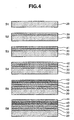
  • Fig. 4 is a sectional view showing manufacturing processes of the piezoelectric actuator of this embodiment; and
  • Fig. 5 is a sectional view showing manufacturing processes of the inkjet recording head serving as a liquid jetting head of this embodiment.
  • Note that in the drawings, the reference symbol 20 refers to a pressure chamber substrate (Si substrate), 30 to a diaphragm, 42 to a bottom electrode, 43 to a piezoelectric thin film, 44 to a top electrode, 21 to a pressure chamber, 10 to a nozzle plate, and 11 to a nozzle.
    BEST MODE FOR CARRYING OUT THE INVENTION (Overall Constitution of Inkjet Printer)
    Fig. 1 is a constitutional diagram of an inkjet printer which is one example of a liquid j etting device comprising a piezoelectric actuator according to an embodiment of the present invention. The inkjet printer mainly comprises an inkjet recording head 1 serving as an example of the liquid jetting head of the present invention, a main body 2, a tray 3, and a head driving mechanism 7.
    The inkjet recording head 1 comprises cartridges storing a total of four colored inks, yellow, magenta, cyan, and black, as liquids to be discharged, and is thus capable of full color printing. This inkjet printer also comprises in its interior a special controller board or the like, bymeans of which ink discharge timing from the inkjet recording head 1 and scanning of the head driving mechanism 7 are controlled.
    A tray 3 is provided on the back face of the main body 2, and an auto sheet feeder (automatic continuous paper supply mechanism) 6 is provided in the interior of the main body 2 for automatically feeding paper 5 and discharging this paper 5 from a discharge port 4 on the front face.
    (Overall Constitution of Inkjet Recording Head)
    Fig. 2 shows an exploded perspective view of the inkjet recording head described above. The inkjet recording head 1 comprises a pressure chamber substrate (Si substrate) 20, a diaphragm 30 which is fixed to one face thereof, and a nozzle plate 10 which is fixed to the other face thereof. This head 1 constitutes an on-demand type piezo jet head.
    The pressure chamber substrate 20 comprises pressure chambers (cavities) 21, side walls (partitions) 22, a reservoir 23, and supply ports 24. The pressure chambers 21 are storage spaces for discharging liquid such as ink. The side walls 22 are formed so as to partition the plurality of pressure chambers 21. The reservoir 23 is a common channel for filling each of the pressure chambers 21 with ink. The supply ports 24 are formed to be capable of leading ink into the pressure chambers 21 from the reservoir 23.
    The nozzle plate 10 is bonded to the pressure chamber substrate 20 such that nozzles 11 formed therein are disposed in positions which correspond to each of the pressure chambers 21 provided in the pressure chamber substrate 20. The pressure chamber substrate 20 bonded with the nozzle plate 10 is housed inside a casing 25.
    A piezoelectric actuator (to be described below) is provided in the diaphragm 30. An ink tank port (not shown) is provided in the diaphragm 30 such that ink stored in the ink tank, not shown in the drawing, can be supplied to the reservoir 23.
    (Layer Structure)
    Fig. 3 is a sectional view illustrating the layer structure of the inkjet recording head and piezoelectric actuator manufactured according to a manufacturing method of the present invention. As shown in the drawing, the piezoelectric actuator is constituted by laminating a diaphragm 30, a buffer layer 41, a bottom electrode 42, a piezoelectric thin film 43, and a top electrode 44 on the (100) orientation Si substrate 20.
    The diaphragm 30 functions to momentarily raise the pressure inside the pressure chambers 21 by deforming in accordance with the deformation of the piezoelectric layer. The diaphragm 30 is constitutedby yttria-stabilized zirconia, CeO2, or ZrO2 in a cubic (100) orientation having a fluorite structure. The yttria-stabilized zirconia, CeO2, or ZrO2 is easily epitaxially grown in a cubic (100) orientation on the (100) Si substrate, and is also suitable for causing the epitaxial growth of the buffer layer thereabove.
    The buffer layer 41 grows epitaxially on the diaphragm 30, and causes the epitaxial growth of the bottom electrode 42 thereabove. The buffer layer 41 is constituted by REBa2Cu3Ox (RE=La, Ce, Pr, Nd, Pm, Sm, Eu, Gd, Tb, Dy, Ho, Er, Tm, Yb, Lu, Y), and undergoes epitaxial growth in a tetragonal or orthorhombic (001) orientation. The buffer layer 41 has a layered perovskite structure comprising a two-dimensional network laminated structure of copper and oxygen.
    The bottom electrode 42 is one of the electrodes for applying a voltage to the piezoelectric thin film layer 43, and is formed in the same region as the diaphragm 30 in order to function as a common electrode for the plurality of piezoelectric thin film elements formed on the pressure chamber substrate 20. Note, however, that the bottom electrode 42 may also be formed with the same magnitude as the piezoelectric thin film layer 43, or in other words in the same shape as the top electrode. The bottom electrode 42 is constituted by a conductive metal oxide, particularly pseudo-cubic (100) orientation strontium ruthenate (SRO). A structure inwhichan iridiumor platinum layer is interposedbetween two SRO layers may also be employed. By interposing an iridium or platinum layer between two SRO layers, tenacity is improved and breakage and cracking can be suppressed.
    The SRO has a perovskite structure, and is expressed by Srn+1RunO3n+1 (where n is an integer of one or more). When n=1, this becomes Sr2RuO4, when n=2 this becomes Sr3Ru2O7, and when n=∞ this becomes SrRuO3. When SRO is used as the bottom electrode in this embodiment, SrRuO3 is most preferable so that conductivity and crystallinity of the piezoelectric thin film can be enhanced. If the constitution described above, in which an iridium or platinum layer is interposed between two SRO layers, is employed, it is particularly preferable to use SrRuO3 for the SRO on the piezoelectric thin film layer side.
    The piezoelectric thin film layer 43 is a piezoelectric ceramic having a perovskite crystalline structure, and is formed in a predetermined shape on top of the bottom electrode 42. As for the composition of the piezoelectric thin film layer 43, lead zirconate titanate (Pb (Zr, Ti) O3: PZT), or a solid solution of leadmagnesiumniobate and lead titanate PMN-PT and a solid solution of lead zinc niobate and lead titanate PZN-PT, or similar is preferable. The composition is not limited thereto, however, and lanthanum-modified lead titanate ((Pb, La) TiO3), lanthanum-modified lead zirconate ((Pb, La) ZrO3), and so on may also be used. The piezoelectric layer of PZT or the like is preferably of a rhombohedral system and has a (100) orientation.
    The top electrode 44 is the other electrode for applying a voltage to the piezoelectric thin film layer 43, and is constituted by a conductive material such as platinum (Pt), iridium (Ir), or aluminum (Al), for example. If aluminum is used, iridium or the like is laminated thereon to prevent electric corrosion.
    (Operations of the Inkjet Recording Head)
    The operations of the aforementioned inkjet recording head 1 will now be described. When no predetermined discharge signal is supplied and a voltage is not appliedbetween the bottom electrode 42 and top electrode 44 of the piezoelectric thin film element 40, no deformation occurs in the piezoelectric thin film layer 43. When no discharge signal is supplied to the piezoelectric thin film element 40, no pressure change is produced in the pressure chamber 21 inwhichthepiezoelectricthin filmelement 40 is provided, and thus no liquiddroplets are discharged from the nozzle 11 thereof.
    However, when a predetermined discharge signal is supplied and a constant voltage is applied between the bottom electrode 42 and top electrode 44 of the piezoelectric thin film element 40, deformation occurs in the piezoelectric thin film layer 43. When a discharge signal is supplied to the piezoelectric thin film element 40, the diaphragm 30 of the pressure chamber 21 in which the piezoelectric thin film element 40 is provided yields greatly. As a result, the pressure inside the pressure chamber 21 rises momentarily, and liquid droplets are discharged from the nozzle 11. By supplying individual discharge signals to piezoelectric elements in positions on the elongated head at which printing is to be performed, desired characters and graphic forms canbe printed.
    (Manufacturing Method)
    Manufacturing processes for the piezoelectric actuator of this embodiment will be described with reference to Fig. 4 in conjunction with a description of the manufacturing processes for the inkjet recording head serving as an example of a liquid jetting head.
    Substrate (S1)
    The piezoelectric actuator of this embodiment is constituted by depositing the diaphragm 30, buffer layer 41, lower electrode 42, piezoelectric thin film 43, and upper electrode 44 onto the pressure chamber substrate 20 shown in Fig. 4 (S1). A (100) orientation silicon single crystal substrate with a diameter of 100mm and a thickness of 200µm, for example, is used as the pressure chamber substrate 20.
    Formation of Diaphragm (S2)
    As is shown in Fig. 4 (S2), the diaphragm 30 constituted by yttria-stabilized zirconia (YSZ) having a composition of Zr1-xYxO2-0.5x (0 ≤ x ≤ 1) or the aforementioned CeO2, ZrO2, or similar is formed on the (100) Si substrate 20 by means of epitaxial growth. Thus a film of YSZ or the like having a (100) orientation is formed.
    The YSZ is set to a thickness of no more than 2µm, for example 1µm. The method for epitaxially forming the diaphragm 30 may be a laser application method, molecular beam epitaxy (MBE), MOCVD, sputtering, or another method.
    Formation of Buffer Layer (S3)
    As shown in Fig. 4 (S3), the buffer layer 41 is deposited on top of the diaphragm 30. REBa2Cu3Ox (RE=La, Ce, Pr, Nd, Pm, Sm, Eu, Gd, Tb, Dy, Ho, Er, Tm, Yb, Lu, Y) is deposited at a thickness of approximately 10nm as the buffer layer 41. A laser application method, for example, is employed as the film deposition method. The method is not limited thereto, however, and a well-known thin film manufacturing method such as MOCVD may be employed.
    Formation of Bottom Electrode (S4)
    As illustrated in Fig. 4 (S4), the bottom electrode 42 is deposited on the buffer layer 41. As the bottom electrode 42, the aforementioned SRO, or a laminated structure of SRO/Pt/SRO or SRO/Ir/SRO is deposited at a thickness of approximately 500nm. A laser application method, for example, may be used as the film deposition method. The method is not limited thereto, however, and a well-known thin film manufacturing method such as MOCVD may be employed.
    Formation of the Piezoelectric Thin Film (S5)
    As is next illustrated in Fig. 4 (S5), the piezoelectric thin film 43 is deposited on top of the bottom electrode 42. In this embodiment, a PZT film constituted by a Pb (Zr0.56Ti0.44) O3 composition is deposited using a sol-gel process, for example. More specifically, an organometallic compound such as a metal alkoxide is subjected to hydrolysis and polycondensation in a solution system to thereby form a piezoelectric precursor film which is an amorphous film. This is then crystallized by calcination.
    The PZT film constituted by a Pb (Zr0.56Ti0.44) O3 composition mayalsobemanufacturedbyanMOD (metal-organicdeposition) method. In this case, hydrolysis of the metal alkoxide is suppressed by the action of an alkanolamine such as triethanolamine or diethanolamine, for example. Other than a metal alkoxide combined with an alkanolamine, a metal acetylacetanate which likewise does not generate electrolysis is suitable as an MOD method starting material. When MOD is used, an identical method to the sol/gel method may be employed in the deposition process. In other words, by undergoing a degreasing process, a piezoelectric precursor film is formed, and this precursor film can be crystallized through calcination.
    The PZT undergoes crystal growth under the influence of the crystalline structure of the SRO bottom electrode. In this embodiment, PZT is deposited on the (100) orientation SRO, and as a result a PZT thin film having a (100) orientation is formed. The thickness of the piezoelectric thin film layer is set at no less than 0.3µm and no more than 2µm, for example.
    If the piezoelectric film is formed by PMN-PT, the composition is one in which the crystal system is rhombohedral, and one in which field-induced bending when a voltage is applied to the piezoelectric body is obtained effectively, or more specifically, a composition of (1-x) Pb (Mg1/3Nb2/3) O3-x PbTiO3, where x satisfies 0.25 ≤ x ≤ 0.35. In particular, x preferably equals 0.3.
    If the piezoelectric film is formed by PZN-PT, the composition is one in which the crystal system is rhombohedral, and one in which field-induced bending when a voltage is applied to the piezoelectric body is obtained effectively, or more specifically, a composition of (1-y) Pb (Zn1/3Nb2/3) O3-y PbTiO3, where y satisfies 0.035 ≤ y ≤ 0.055. In particular, y preferably equals 0.045.
    PMN-PT and PZN-PT also form films exhibiting a (100) orientation on the SRO. The thickness of the piezoelectric film is set at no less than 0.3µm and no more than 2µm, for example.
    Formation of Top Electrode (S6)
    As is next illustrated in Fig. 4 (S6), the top electrode 44 is formed on top of the piezoelectric thin film 43. More specifically, platinum (Pt) or the like is deposited as the top electrode 44 at a film thickness of 100nm by means of DC sputtering.
    (Formation of Piezoelectric Actuator)
    As illustrated in Fig. 5 (S7), the piezoelectric thin film 43 and top electrode 44 are worked into a predetermined shape to form a piezoelectric actuator. More specifically, resist is spin-coated onto the top electrode 44, whereupon the resist is patterned by exposure and development in alignment with the positions at which the pressure chambers are to be formed. With the remaining resist as a mask, the top electrode 44 and the piezoelectric thin film 43 are etched by ion milling or the like. By means of this process, a piezoelectric actuator comprising piezoelectric thin film elements 40 is formed.
    (Formation of the Inkjet Recording Head)
    As illustrated in Fig. 5 (S8), pressure chambers 21 are formed in the pressure chamber substrate 20. When a (100) orientation Si substrate is used as the pressure chamber substrate 20, dry etching is used as the formation method of the pressure chambers 21. The remaining parts that are not etched become the side walls 22.
    Finally, as illustrated in Fig. 5 (S9), the nozzle plate 10 is bonded to the pressure chamber substrate 20 using resin or the like. When the nozzle plate 10 is to be bonded to the pressure chamber substrate 20, the position of the nozzle plate 10 is aligned such that the nozzles 11 are disposed corresponding to each of the spaces in the pressure chambers 21. By means of this process, the inkjet recording head is formed.
    (Other Applications)
    The present inventionmaybe applied in various modifications other than this embodiment. For example, the piezoelectric actuator of the present invention may be applied not only as the liquid jetting head described above, but as various other actuators such as a precision positioning mechanism such as an STM, a cell manipulator, a probe for an ultrasound diagnostic device, an ultrasonic motor, and a small bimor pump.
    The liquid jetting head of the present invention may also be applied to various heads for discharging a liquid other than a head for discharging ink used in an inkjet recording device, for example a head for discharging liquid containing coloring material used in the manufacture of color filters for liquid crystal displays and the like, a head for discharging liquid containing electrode material used to form electrodes for organic EL displays, FEDs (field emission displays), and the like, a head for discharging liquid containing bioorganic substances used in the manufacture of biochips, and so on.
    INDUSTRIAL APPLICABILITY
    According to the present invention, a piezoelectric actuator having an optimum layer structure can be provided for a case in which (100) orientation strontium ruthenate is used as a bottom electrode. A liquid jetting head comprising this piezoelectric actuator can also be provided.

    Claims (6)

    1. A piezoelectric actuator characterized in comprising:
      a diaphragm that is constituted by yttria-stabilized zirconia, CeO2, or ZrO2, that is grown epitaxially on a (100) orientation Si substrate in a cubic (100) orientation having a fluorite structure;
      abuffer layer formed on said diaphragm and constituted by tetragonal or orthorhombic (001) orientation REBa2Cu3Ox having a layered perovskite structure (RE=La, Ce, Pr, Nd, Pm, Sm, Eu, Gd, Tb, Dy, Ho, Er, Tm, Yb, Lu, Y);
      a bottom electrode formed on said buffer layer and constituted by pseudo-cubic (100) orientation strontium ruthenate having a perovskite structure;
      a piezoelectric layer formed on said bottom electrode and having a rhombohedral (100) orientation perovskite structure; and
      a top electrode formed on said piezoelectric layer.
    2. The piezoelectric actuator according to claim 1, characterized in that said bottom electrode comprises at least two layers of strontium ruthenate and a layer of iridium or platinum interposed therebetween.
    3. The piezoelectric actuator according to claim 1 or 2, characterized in that of the strontium ruthenate constituting said bottom electrode, at least the layer on the side of said piezoelectric layer has a composition expressed by SrRuO3.
    4. The piezoelectric actuator according to any of claims 1 through 3, characterized in that said piezoelectric layer is PZT, PMN-PT, or PZN-PT.
    5. A liquid jetting head characterized in comprising:
      the piezoelectric actuator according to any of claims 1 through 4; and
      a pressure chamber provided on said Si substrate and constituting a capacity which is variable in accordance with the oscillation of said diaphragm comprised in said piezoelectric actuator.
    6. A liquid jetting device, characterized in comprising the liquid jetting head according to claim 5 as liquid jetting means.
    EP20030725789 2002-05-15 2003-05-15 PIEZOELECTRIC ACTUATOR AND INKJET HEAD Withdrawn EP1505663A4 (en)

    Applications Claiming Priority (3)

    Application Number Priority Date Filing Date Title
    JP2002140558 2002-05-15
    JP2002140558 2002-05-15
    PCT/JP2003/006074 WO2003098714A1 (en) 2002-05-15 2003-05-15 Piezoelectric actuator and liquid jet head

    Publications (2)

    Publication Number Publication Date
    EP1505663A1 true EP1505663A1 (en) 2005-02-09
    EP1505663A4 EP1505663A4 (en) 2009-08-19

    Family

    ID=29544929

    Family Applications (1)

    Application Number Title Priority Date Filing Date
    EP20030725789 Withdrawn EP1505663A4 (en) 2002-05-15 2003-05-15 PIEZOELECTRIC ACTUATOR AND INKJET HEAD

    Country Status (5)

    Country Link
    US (1) US7279823B2 (en)
    EP (1) EP1505663A4 (en)
    JP (1) JP4432776B2 (en)
    CN (1) CN100421275C (en)
    WO (1) WO2003098714A1 (en)

    Cited By (2)

    * Cited by examiner, † Cited by third party
    Publication number Priority date Publication date Assignee Title
    EP1677368A3 (en) * 2004-12-28 2007-07-11 Seiko Epson Corporation Piezoelectric devices with conductive perovskite layers
    EP1396877B1 (en) * 2002-09-05 2008-11-26 Seiko Epson Corporation Substrate for electronic devices, manufacturing method therefor, and electronic device

    Families Citing this family (40)

    * Cited by examiner, † Cited by third party
    Publication number Priority date Publication date Assignee Title
    JP2004281742A (en) * 2003-03-17 2004-10-07 Japan Science & Technology Agency Semiconductor device, semiconductor sensor and semiconductor storage device
    US7411339B2 (en) * 2003-11-28 2008-08-12 Seiko Epson Corporation Manufacturing method of actuator device and liquid jet apparatus provided with actuator device formed by manufacturing method of the same
    JP4717344B2 (en) * 2003-12-10 2011-07-06 キヤノン株式会社 Dielectric thin film element, piezoelectric actuator, and liquid discharge head
    JP5013035B2 (en) * 2003-12-11 2012-08-29 セイコーエプソン株式会社 Dielectric film manufacturing method and liquid jet head manufacturing method
    JP4192794B2 (en) 2004-01-26 2008-12-10 セイコーエプソン株式会社 Piezoelectric element, piezoelectric actuator, ink jet recording head, ink jet printer, surface acoustic wave element, frequency filter, oscillator, electronic circuit, thin film piezoelectric resonator, and electronic device
    TWI253392B (en) * 2004-03-29 2006-04-21 Canon Kk Dielectric member, piezoelectric member, ink jet head, ink jet recording apparatus and producing method for ink jet recording apparatus
    US7235917B2 (en) * 2004-08-10 2007-06-26 Canon Kabushiki Kaisha Piezoelectric member element and liquid discharge head comprising element thereof
    JP2006093042A (en) * 2004-09-27 2006-04-06 Seiko Epson Corp Ferroelectric thin film forming composition, ferroelectric thin film, and liquid jet head
    KR100639918B1 (en) 2004-12-16 2006-11-01 한국전자통신연구원 MEMS Actuator
    JP4793568B2 (en) * 2005-07-08 2011-10-12 セイコーエプソン株式会社 Actuator device, liquid jet head, and liquid jet device
    JP2009542285A (en) * 2006-06-28 2009-12-03 コーニンクレッカ フィリップス エレクトロニクス エヌ ヴィ Apparatus and method for supplying high speed microjet fluid
    JP2010238856A (en) * 2009-03-31 2010-10-21 Tdk Corp Piezoelectric element and gyro sensor
    JP5585209B2 (en) 2009-05-28 2014-09-10 株式会社リコー Electromechanical transducer manufacturing method, electromechanical transducer manufactured by the manufacturing method, droplet ejection head, and droplet ejection apparatus
    JP5110052B2 (en) * 2009-07-24 2012-12-26 セイコーエプソン株式会社 Actuator device, liquid jet head, and liquid jet device
    JP2011061117A (en) * 2009-09-14 2011-03-24 Seiko Epson Corp Piezoelectric element, piezoelectric actuator, liquid injection head, and liquid injection apparatus
    JP5660288B2 (en) * 2010-01-05 2015-01-28 セイコーエプソン株式会社 Liquid ejecting head, liquid ejecting apparatus, piezoelectric element, and liquid ejecting head manufacturing method
    JP5423414B2 (en) * 2010-01-15 2014-02-19 株式会社リコー Electromechanical conversion film manufacturing method, electromechanical conversion film, electromechanical conversion film group, electromechanical conversion element manufacturing method, electromechanical conversion element, electromechanical conversion element group, liquid discharge head, liquid discharge apparatus, and image forming apparatus
    JP5526810B2 (en) 2010-01-28 2014-06-18 株式会社リコー Sol-gel liquid, electro-mechanical conversion element, liquid discharge head, and ink jet recording apparatus
    JP2012059770A (en) * 2010-09-06 2012-03-22 Seiko Epson Corp Piezoelectric element, liquid ejecting head, liquid ejecting apparatus, and methods for the manufacture thereof
    WO2012036103A1 (en) * 2010-09-15 2012-03-22 Ricoh Company, Ltd. Electromechanical transducing device and manufacturing method thereof, and liquid droplet discharging head and liquid droplet discharging apparatus
    JP2012256756A (en) 2011-06-09 2012-12-27 Ricoh Co Ltd Formation method of electromechanical conversion film, electromechanical conversion film, electromechanical conversion element, liquid discharge head and image forming apparatus
    CN102983772A (en) * 2011-09-05 2013-03-20 研能科技股份有限公司 Drive circuit and piezo-actuated pump for which it is applied
    US9761785B2 (en) 2011-10-17 2017-09-12 The United States Of America As Represented By The Secretary Of The Army Stylo-epitaxial piezoelectric and ferroelectric devices and method of manufacturing
    US8866367B2 (en) 2011-10-17 2014-10-21 The United States Of America As Represented By The Secretary Of The Army Thermally oxidized seed layers for the production of {001} textured electrodes and PZT devices and method of making
    JP2014198398A (en) * 2013-03-29 2014-10-23 セイコーエプソン株式会社 Flow path unit, liquid ejecting head, liquid ejecting apparatus, and manufacturing method of flow path unit
    JP5761540B2 (en) 2013-06-28 2015-08-12 セイコーエプソン株式会社 Piezoelectric material, piezoelectric element, liquid ejecting head, liquid ejecting apparatus, ultrasonic sensor, piezoelectric motor, and power generation apparatus
    JP5754660B2 (en) * 2013-06-28 2015-07-29 セイコーエプソン株式会社 Piezoelectric material, piezoelectric element, liquid ejecting head, liquid ejecting apparatus, ultrasonic sensor, piezoelectric motor, and power generation apparatus
    JP2015038953A (en) 2013-06-28 2015-02-26 セイコーエプソン株式会社 Piezoelectric material, piezoelectric element, liquid injection head, liquid injection device, ultrasonic sensor, piezoelectric motor and power generator
    JP6287121B2 (en) 2013-11-28 2018-03-07 株式会社リコー Electro-mechanical conversion film manufacturing method, electro-mechanical conversion element, liquid discharge head, ink jet recording apparatus
    JP6244865B2 (en) * 2013-12-09 2017-12-13 船井電機株式会社 Vibration mirror element
    JP6442860B2 (en) 2014-04-23 2018-12-26 株式会社リコー Precursor sol-gel solution, electromechanical transducer, droplet discharge head, and ink jet recording apparatus
    EP3240055B1 (en) 2014-12-26 2021-06-23 Seiko Epson Corporation Piezoelectric material and method for producing same, piezoelectric element, and device using piezoelectric element
    WO2017083150A1 (en) * 2015-11-13 2017-05-18 IQE, plc Layer structures for rf filters fabricated using rare earth oxides and epitaxial aluminum nitride
    US11495670B2 (en) 2016-09-22 2022-11-08 Iqe Plc Integrated epitaxial metal electrodes
    KR102400476B1 (en) 2016-09-22 2022-05-20 아이큐이, 피엘씨 Integrated epitaxial metal electrode
    US10418457B2 (en) 2016-09-22 2019-09-17 Iqe Plc Metal electrode with tunable work functions
    JP6910631B2 (en) * 2016-11-15 2021-07-28 アドバンストマテリアルテクノロジーズ株式会社 Membrane structure and its manufacturing method
    JP6881790B2 (en) * 2017-05-26 2021-06-02 アドバンストマテリアルテクノロジーズ株式会社 Membrane structure and its manufacturing method
    JP7210253B2 (en) * 2018-12-06 2023-01-23 株式会社堀場エステック fluid control valve
    CN120191128A (en) * 2023-12-22 2025-06-24 苏州众行汇创科技有限公司 Liquid ejection head and liquid ejection device including the same

    Family Cites Families (12)

    * Cited by examiner, † Cited by third party
    Publication number Priority date Publication date Assignee Title
    US5179070A (en) * 1988-04-30 1993-01-12 Sumitomo Electric Industries, Ltd. Semiconductor substrate having a superconducting thin film with a buffer layer in between
    US5529981A (en) * 1992-03-05 1996-06-25 Holloway; Alex Process and apparatus for preparing biaxially textured materials using anisotropy in the paramagnetic susceptibility
    US5270298A (en) * 1992-03-05 1993-12-14 Bell Communications Research, Inc. Cubic metal oxide thin film epitaxially grown on silicon
    JP2001509312A (en) 1997-01-28 2001-07-10 ザ ペンステート リサーチファウンデーション Relaxor ferroelectric single crystal for ultrasonic transducer
    JP3472087B2 (en) * 1997-06-30 2003-12-02 Tdk株式会社 Film structure, electronic device, recording medium, and method for producing oxide conductive thin film
    US5889289A (en) * 1997-08-28 1999-03-30 The United States Of America As Represented By The Secretary Of The Navy High temperature superconductor/insulator composite thin films with Josephson coupled grains
    JP4006562B2 (en) * 2000-02-21 2007-11-14 セイコーエプソン株式会社 Piezoelectric element, ink jet recording head, manufacturing method thereof, and ink jet printer
    JP3796394B2 (en) * 2000-06-21 2006-07-12 キヤノン株式会社 Method for manufacturing piezoelectric element and method for manufacturing liquid jet recording head
    JP3817729B2 (en) * 2001-11-08 2006-09-06 セイコーエプソン株式会社 Piezoelectric actuator and liquid discharge head
    JP4228569B2 (en) * 2001-11-28 2009-02-25 セイコーエプソン株式会社 Method for manufacturing substrate for electronic device and method for manufacturing electronic device
    JP2003179279A (en) * 2001-12-10 2003-06-27 Seiko Epson Corp Piezoelectric actuator and ink jet recording head
    GB0218261D0 (en) * 2002-08-06 2002-09-11 Charterhouse Therapeutics Ltd Improvements in pharmaceutically useful compounds

    Cited By (3)

    * Cited by examiner, † Cited by third party
    Publication number Priority date Publication date Assignee Title
    EP1396877B1 (en) * 2002-09-05 2008-11-26 Seiko Epson Corporation Substrate for electronic devices, manufacturing method therefor, and electronic device
    EP1677368A3 (en) * 2004-12-28 2007-07-11 Seiko Epson Corporation Piezoelectric devices with conductive perovskite layers
    US7622850B2 (en) 2004-12-28 2009-11-24 Seiko Epson Corporation Piezoelectric device, piezoelectric actuator, piezoelectric pump, inkjet recording head, inkjet printer, surface acoustic wave device, thin-film piezoelectric resonator, frequency filter, oscillator, electronic circuit, and electronic instrument

    Also Published As

    Publication number Publication date
    CN1579025A (en) 2005-02-09
    EP1505663A4 (en) 2009-08-19
    JPWO2003098714A1 (en) 2005-09-22
    CN100421275C (en) 2008-09-24
    JP4432776B2 (en) 2010-03-17
    WO2003098714A1 (en) 2003-11-27
    US7279823B2 (en) 2007-10-09
    US20050179342A1 (en) 2005-08-18

    Similar Documents

    Publication Publication Date Title
    US7279823B2 (en) Piezoelectric actuator and liquid jet head
    US7033521B2 (en) Piezoelectric actuator, ink jet head, and discharge apparatus
    KR100643825B1 (en) Dielectric thin film element, piezoelectric actuator and liquid discharge head, and method for manufacturing the same
    US8733906B2 (en) Electromechanical conversion element, liquid drop ejection head, liquid drop ejection device, and image forming apparatus
    US7589450B2 (en) Actuator device, liquid-jet head and liquid-jet apparatus
    JP6525255B2 (en) Electro-mechanical transducer, method of manufacturing electro-mechanical transducer, droplet discharge head and droplet discharge device
    US7562968B2 (en) Piezoelectric element, liquid-jet head and liquid-jet apparatus
    CN102649357A (en) Ink-jet head and ink-jet recording apparatus
    JP4708667B2 (en) Actuator and liquid jet head
    JP4099818B2 (en) Piezoelectric actuator and ink jet recording head
    JP3902023B2 (en) Piezoelectric actuator, liquid droplet ejecting head, and liquid droplet ejecting apparatus using the same
    US7497962B2 (en) Method of manufacturing liquid discharge head and method of manufacturing substrate for liquid discharge head
    JP3828116B2 (en) Piezoelectric element
    US6779878B2 (en) Piezoelectronic actuator and liquid jetting head
    TW201711235A (en) Piezoelectric device, liquid ejecting head, liquid ejecting apparatus, and manufacturing method of piezoelectric device
    US7399066B2 (en) Piezoelectric element, ink jet recording head and producing method for piezoelectric element
    JP2005340428A (en) Piezoelectric element and manufacturing method thereof
    JP2003179279A (en) Piezoelectric actuator and ink jet recording head
    JP2003152233A (en) Piezoelectric actuator and ink jet recording head
    JP2014157850A (en) Electromechanical conversion element, droplet discharge head, and image forming apparatus
    JP4086864B2 (en) Method for manufacturing liquid discharge head and method for manufacturing substrate for liquid discharge head
    JP5998537B2 (en) Electro-mechanical conversion element, droplet discharge head, and droplet discharge apparatus
    JP2004128174A (en) Actuator and liquid jet head

    Legal Events

    Date Code Title Description
    PUAI Public reference made under article 153(3) epc to a published international application that has entered the european phase

    Free format text: ORIGINAL CODE: 0009012

    17P Request for examination filed

    Effective date: 20040503

    AK Designated contracting states

    Kind code of ref document: A1

    Designated state(s): AT BE BG CH CY CZ DE DK EE ES FI FR GB GR HU IE IT LI LU MC NL PT RO SE SI SK TR

    A4 Supplementary search report drawn up and despatched

    Effective date: 20090720

    RIC1 Information provided on ipc code assigned before grant

    Ipc: B41J 2/055 20060101ALI20031203BHEP

    Ipc: B41J 2/045 20060101ALI20031203BHEP

    Ipc: H01L 41/09 20060101AFI20090714BHEP

    STAA Information on the status of an ep patent application or granted ep patent

    Free format text: STATUS: THE APPLICATION HAS BEEN WITHDRAWN

    18W Application withdrawn

    Effective date: 20090902