EP1503500B1 - Boucle à verrouillage de phase - Google Patents
Boucle à verrouillage de phase Download PDFInfo
- Publication number
- EP1503500B1 EP1503500B1 EP20040447092 EP04447092A EP1503500B1 EP 1503500 B1 EP1503500 B1 EP 1503500B1 EP 20040447092 EP20040447092 EP 20040447092 EP 04447092 A EP04447092 A EP 04447092A EP 1503500 B1 EP1503500 B1 EP 1503500B1
- Authority
- EP
- European Patent Office
- Prior art keywords
- frequency
- signal
- phase
- filter
- mixer
- Prior art date
- Legal status (The legal status is an assumption and is not a legal conclusion. Google has not performed a legal analysis and makes no representation as to the accuracy of the status listed.)
- Expired - Lifetime
Links
- 230000014509 gene expression Effects 0.000 description 7
- 230000000630 rising effect Effects 0.000 description 5
- 230000002238 attenuated effect Effects 0.000 description 2
- 230000007423 decrease Effects 0.000 description 2
- 238000000034 method Methods 0.000 description 2
- 229920000729 poly(L-lysine) polymer Polymers 0.000 description 2
- 238000011084 recovery Methods 0.000 description 2
- 230000007704 transition Effects 0.000 description 2
- 238000001914 filtration Methods 0.000 description 1
- 230000001105 regulatory effect Effects 0.000 description 1
Images


Classifications
-
- H—ELECTRICITY
- H03—ELECTRONIC CIRCUITRY
- H03L—AUTOMATIC CONTROL, STARTING, SYNCHRONISATION OR STABILISATION OF GENERATORS OF ELECTRONIC OSCILLATIONS OR PULSES
- H03L7/00—Automatic control of frequency or phase; Synchronisation
- H03L7/06—Automatic control of frequency or phase; Synchronisation using a reference signal applied to a frequency- or phase-locked loop
- H03L7/16—Indirect frequency synthesis, i.e. generating a desired one of a number of predetermined frequencies using a frequency- or phase-locked loop
- H03L7/18—Indirect frequency synthesis, i.e. generating a desired one of a number of predetermined frequencies using a frequency- or phase-locked loop using a frequency divider or counter in the loop
- H03L7/183—Indirect frequency synthesis, i.e. generating a desired one of a number of predetermined frequencies using a frequency- or phase-locked loop using a frequency divider or counter in the loop a time difference being used for locking the loop, the counter counting between fixed numbers or the frequency divider dividing by a fixed number
- H03L7/185—Indirect frequency synthesis, i.e. generating a desired one of a number of predetermined frequencies using a frequency- or phase-locked loop using a frequency divider or counter in the loop a time difference being used for locking the loop, the counter counting between fixed numbers or the frequency divider dividing by a fixed number using a mixer in the loop
-
- H—ELECTRICITY
- H03—ELECTRONIC CIRCUITRY
- H03L—AUTOMATIC CONTROL, STARTING, SYNCHRONISATION OR STABILISATION OF GENERATORS OF ELECTRONIC OSCILLATIONS OR PULSES
- H03L7/00—Automatic control of frequency or phase; Synchronisation
- H03L7/06—Automatic control of frequency or phase; Synchronisation using a reference signal applied to a frequency- or phase-locked loop
- H03L7/08—Details of the phase-locked loop
- H03L7/085—Details of the phase-locked loop concerning mainly the frequency- or phase-detection arrangement including the filtering or amplification of its output signal
- H03L7/089—Details of the phase-locked loop concerning mainly the frequency- or phase-detection arrangement including the filtering or amplification of its output signal the phase or frequency detector generating up-down pulses
- H03L7/0891—Details of the phase-locked loop concerning mainly the frequency- or phase-detection arrangement including the filtering or amplification of its output signal the phase or frequency detector generating up-down pulses the up-down pulses controlling source and sink current generators, e.g. a charge pump
Definitions
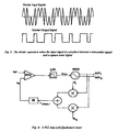
- a Phase Locked loop is an electronics circuit, intended to generate an electrical signal with a given frequency.
- An example of such a circuit is depicted in Fig. 1.
- the PLL mainly contains a Voltage-controlled Oscillator (VCO), a frequency divider (/N), a Phase-comparator (or Phase-Frequency comparator - PFC 1 ) and a loop filter (LPF).
- VCO Voltage-controlled Oscillator
- /N frequency divider
- Phase-comparator or Phase-Frequency comparator - PFC 1
- LPF loop filter
- the basic function of PFC is to control the VCO input signal V vco in such a way that the two inputs Ref and FB evolve to a state where they are oscillating in phase and hence, their frequencies are equal. This is called the "locked" state.
- This PLL can be used to create an output signal with a frequency that is N times larger than the frequency of the reference signal 2 .
- a PLL can be used for other purposes, such as FM modulation or demodulation, phase (de)modulation or clock recovery. These items are beyond the scope of this explanation, although the present invention can be used also in these domains.
- a PLL can be used for other purposes, such as FM modulation or demodulation, phase (de)modulation or clock recovery. These items are beyond the scope of this explanation, although the present invention can be used also in these domains.
- Element 1 a Single-Sideband Mixer
- a VCO is the VCO output signal amplitude.
- Element 2 a Tracking filter
- a second element of the invention aims to eliminate the fast transitions in the signal divider input signal of Fig. 5. These are due to the fact that the signals v B,I ,F and v B,Q are square wave signals instead of sinusoidal signals.
- An obvious solution to this problem is to place a lowpass filter at the mixer output. In this way, the fast voltage transitions at the mixer output are filtered out, resulting in a clean sinusoidal signal.
- the mixer output signal frequency can vary over a large range.
- the PLL division factor is programmable, to generate a programmable PLL output frequency.
- the mixer output frequency can vary over a wide range.
- the present invention proposes a tracking filter where the cut-off frequency is continuously adapted to a value that is suited for the current situation.
- This is shown in Fig. 7.
- This figure shows a lowpass filter, where the filter cut-off frequency is determined by the signal V c . This signal is controlled continuously in such a way that the filter cut-off frequency is continuously set to a correct value.
- a continuous-time filter also called a "gm-C” filter, a “transconductance-C” filter or a “gyrator” filter
- a control signal a voltage or a current
- a continuous-time filter also called a "gm-C” filter, a “transconductance-C” filter or a “gyrator” filter
- the filter output signal amplitude is measured with a peak detector (or an RMS detector).
- the filter input signal amplitude is measured.
- the voltage v c it is possible to control the voltage v c in such a way that the output signal amplitude is e.g. half the value of the input signal amplitude.
- Element 3 a double-quadrature mixer with phase detector
- the PLL can obtain a lock condition for output frequencies that satisfy either expression (3) or (4).
- Fig. 10 a circuit is shown that eliminates one of the two possibilities:
- This circuit contains a double-quadrature mixer, producing two output signals according to the expressions (7) and (8):
- V mixer,I When f out > f B , V mixer,I has a 90° phase advance compared to V mixer,Q : at a rising zero-crossing of V mixer,I , V mixer,Q is negative.
- V mixer,I has a 90° phase lag compared to V mixer,Q at a rising zero-crossing of V mixer,I , V mixer,Q is positive
- the circuit of Fig. 10 allows to discriminate between these two cases: when f out > f B , the digital signal S is high, but when f out ⁇ f B , signal S is low.
- This digital signal is used to modify the behaviour of the Phase-frequency comparator.
- Fig. 11 (left), an example of such a Phase-frequency comparator is shown.
- signal "UP” When signal "UP” is high, the VCO frequency is increased, while an active signal “DOWN” decreases the VCO frequency.
- UP and DOWN are (almost) never active simultaneously.
- S when S is low, the signal UP is constantly forced active while DOWN is never active.
- the VCO output frequency will increase until S becomes high, i.e. until f out > f B .
- the phase-frequency comparator resumes its normal behaviour, and the PLL output frequency will evolve to the value given by expression (3). This is the only possible stable output frequency.
Landscapes
- Stabilization Of Oscillater, Synchronisation, Frequency Synthesizers (AREA)
Claims (7)
- Boucle à verrouillage de phase comprenant un comparateur de phase (PFC) ayant une première entrée et une deuxième entrée, un filtre de boucle (LPF) et un oscillateur commandé par tension (VCO) couplés en série, ledit VCO délivrant un signal en phase et un signal en quadrature à une première fréquence, et comprenant en outre un mélangeur en double quadrature, ledit mélangeur en double quadrature étant alimenté par ledit signal en phase et ledit signal en quadrature à ladite première fréquence et par un signal en phase et un signal en quadrature à une deuxième fréquence, ledit mélangeur en double quadrature générant un signal en phase et en quadrature à une fréquence qui est la différence entre ladite première et ladite deuxième fréquence, ledit signal en phase ou ledit signal en quadrature à ladite fréquence de différence étant en outre appliqué à un diviseur de fréquence, la sortie dudit diviseur de fréquence étant acheminée à ladite première entrée dudit PFC, caractérisée en ce qu'un signal numérique S dérivé dudit signal en phase et dudit signal en quadrature à ladite fréquence de différence est acheminé audit PFC par une troisième entrée, ledit signal numérique comprenant des informations indiquant si ladite première fréquence est plus élevée ou non que ladite deuxième fréquence.
- Boucle à verrouillage de phase selon la revendication 1, dans laquelle lesdites informations comprises dans ledit signal numérique sont déduites de la phase dudit signal en phase et dudit signal en quadrature à ladite fréquence de différence.
- Boucle à verrouillage de phase selon la revendication 2, comprenant en outre une bascule bistable numérique pour déduire lesdites informations comprises dans ledit signal numérique.
- Boucle à verrouillage de phase comprenant un comparateur de phase (PFC) ayant une première entrée et une deuxième entrée, un filtre de boucle (LPF) et un oscillateur commandé par tension (VCO) couplés en série, et comprenant en outre un mélangeur, ledit mélangeur étant alimenté par un signal à une première fréquence, ledit signal étant délivré par ledit VCO, et par un signal à une deuxième fréquence, ledit mélangeur générant un signal à une fréquence qui est la différence entre ladite première et ladite deuxième fréquence, caractérisée en ce que ledit signal généré par ledit mélangeur est en outre acheminé à un filtre ayant une fréquence de coupure variable, ladite fréquence de coupure variable étant commandée par un signal de commande de filtre (Vc), la sortie dudit filtre à fréquence de coupure variable étant acheminée à un diviseur de fréquence, ladite sortie du diviseur de fréquence étant acheminée à ladite première entrée dudit comparateur de phase (PFC).
- Boucle à verrouillage de phase selon la revendication 4, dans laquelle ledit filtre à fréquence de coupure variable est un filtre gm-C.
- Boucle à verrouillage de phase selon la revendication 4 ou 5, dans laquelle ledit signal de commande de filtre (Vc) est aménagé pour conserver l'amplitude de ladite sortie dudit filtre à fréquence de coupure variable à une valeur donnée.
- Boucle à verrouillage de phase selon la revendication 4 ou 5, dans laquelle ledit signal de commande de filtre (Vc) est aménagé pour conserver le rapport entre l'amplitude du signal de sortie et l'amplitude du signal d'entrée dudit filtre à une valeur donnée.
Priority Applications (1)
| Application Number | Priority Date | Filing Date | Title |
|---|---|---|---|
| EP20040447092 EP1503500B1 (fr) | 2003-07-28 | 2004-04-08 | Boucle à verrouillage de phase |
Applications Claiming Priority (3)
| Application Number | Priority Date | Filing Date | Title |
|---|---|---|---|
| BE200344719 | 2003-07-28 | ||
| EP03447199 | 2003-07-28 | ||
| EP20040447092 EP1503500B1 (fr) | 2003-07-28 | 2004-04-08 | Boucle à verrouillage de phase |
Publications (2)
| Publication Number | Publication Date |
|---|---|
| EP1503500A1 EP1503500A1 (fr) | 2005-02-02 |
| EP1503500B1 true EP1503500B1 (fr) | 2006-06-28 |
Family
ID=34178717
Family Applications (1)
| Application Number | Title | Priority Date | Filing Date |
|---|---|---|---|
| EP20040447092 Expired - Lifetime EP1503500B1 (fr) | 2003-07-28 | 2004-04-08 | Boucle à verrouillage de phase |
Country Status (1)
| Country | Link |
|---|---|
| EP (1) | EP1503500B1 (fr) |
Families Citing this family (1)
| Publication number | Priority date | Publication date | Assignee | Title |
|---|---|---|---|---|
| US7949072B2 (en) * | 2005-10-11 | 2011-05-24 | St-Ericsson Sa | Local oscillator with injection pulling suppression and spurious products filtering |
Family Cites Families (3)
| Publication number | Priority date | Publication date | Assignee | Title |
|---|---|---|---|---|
| FR2581277A1 (fr) * | 1985-04-30 | 1986-10-31 | Labo Electronique Physique | Circuit de recuperation de l'onde porteuse de systemes de transmissions numeriques |
| FR2677824B1 (fr) * | 1991-06-14 | 1993-08-20 | Thomson Csf | Dispositif de controle d'une boucle de phase a changement de frequence. |
| GB2282030B (en) * | 1993-09-14 | 1997-09-24 | Plessey Semiconductors Ltd | Direct conversion receiver |
-
2004
- 2004-04-08 EP EP20040447092 patent/EP1503500B1/fr not_active Expired - Lifetime
Also Published As
| Publication number | Publication date |
|---|---|
| EP1503500A1 (fr) | 2005-02-02 |
Similar Documents
| Publication | Publication Date | Title |
|---|---|---|
| US6731709B2 (en) | Phase locked loop and method that provide fail-over redundant clocking | |
| US10790839B2 (en) | Device for adjusting the locking of an injection locked frequency multiplier | |
| EP2571165B1 (fr) | Synthétiseur à boucle à verrouillage de phase fractionnaire du type accumulateur et procédé de commande de celui-ci | |
| US6211743B1 (en) | Phase-locked loop having temperature-compensated bandwidth control | |
| Gawa et al. | A 50% duty-cycle correction circuit for PLL output | |
| US6753711B2 (en) | Digital summing phase-lock loop circuit with sideband control and method therefor | |
| US20050104667A1 (en) | Frequency synthesizer having PLL with an analog phase detector | |
| US8638141B1 (en) | Phase-locked loop | |
| EP1503500B1 (fr) | Boucle à verrouillage de phase | |
| JPS58182323A (ja) | 位相同期回路 | |
| US20040151271A1 (en) | Phase-locked loop control circuit | |
| Zhuang et al. | A 4GHz low complexity ADPLL-based frequency synthesizer in 90nm CMOS | |
| CN107683569B (zh) | 频率检测器 | |
| WO2003052936A1 (fr) | Ameliorations apportees a la synthese de frequence | |
| US20070237277A1 (en) | Method and Integrated Circuit for Controlling an Oscillator Signal | |
| Dinesh et al. | A Survey on ADPLL Components and their effects upon Power, Frequency and Resolution | |
| US5339049A (en) | Ultra low noise frequency divider/multiplier | |
| Hur et al. | A low jitter phase-lock loop based on a new adaptive bandwidth controller | |
| Ramekar et al. | Design and analysis of frequency synthesizer with low power ring oscillator for wireless application | |
| Maddy et al. | The Electrical Engineering Handbook Ed. Richard C. Dorf Boca Raton: CRC Press LLC, 2000 | |
| Yim | An integer-N charge-pump phase-locked loop with controllable phase offset | |
| SANTIAGO | Design of Analog Phase-Locked Loops (A tutorial) | |
| Choudhary et al. | Phase-Locked Loop—Based Integer-N RF Synthesizer | |
| US20060220712A1 (en) | Frequency double circuit | |
| JP6062841B2 (ja) | 注入型位相同期回路 |
Legal Events
| Date | Code | Title | Description |
|---|---|---|---|
| PUAI | Public reference made under article 153(3) epc to a published international application that has entered the european phase |
Free format text: ORIGINAL CODE: 0009012 |
|
| AK | Designated contracting states |
Kind code of ref document: A1 Designated state(s): AT BE BG CH CY CZ DE DK EE ES FI FR GB GR HU IE IT LI LU MC NL PL PT RO SE SI SK TR |
|
| AX | Request for extension of the european patent |
Extension state: AL HR LT LV MK |
|
| 17P | Request for examination filed |
Effective date: 20050801 |
|
| AKX | Designation fees paid |
Designated state(s): AT BE BG CH CY CZ DE DK EE ES FI FR GB GR HU IE IT LI LU MC NL PL PT RO SE SI SK TR |
|
| GRAP | Despatch of communication of intention to grant a patent |
Free format text: ORIGINAL CODE: EPIDOSNIGR1 |
|
| GRAS | Grant fee paid |
Free format text: ORIGINAL CODE: EPIDOSNIGR3 |
|
| GRAA | (expected) grant |
Free format text: ORIGINAL CODE: 0009210 |
|
| AK | Designated contracting states |
Kind code of ref document: B1 Designated state(s): AT BE BG CH CY CZ DE DK EE ES FI FR GB GR HU IE IT LI LU MC NL PL PT RO SE SI SK TR |
|
| PG25 | Lapsed in a contracting state [announced via postgrant information from national office to epo] |
Ref country code: IT Free format text: LAPSE BECAUSE OF FAILURE TO SUBMIT A TRANSLATION OF THE DESCRIPTION OR TO PAY THE FEE WITHIN THE PRESCRIBED TIME-LIMIT;WARNING: LAPSES OF ITALIAN PATENTS WITH EFFECTIVE DATE BEFORE 2007 MAY HAVE OCCURRED AT ANY TIME BEFORE 2007. THE CORRECT EFFECTIVE DATE MAY BE DIFFERENT FROM THE ONE RECORDED. Effective date: 20060628 Ref country code: PL Free format text: LAPSE BECAUSE OF FAILURE TO SUBMIT A TRANSLATION OF THE DESCRIPTION OR TO PAY THE FEE WITHIN THE PRESCRIBED TIME-LIMIT Effective date: 20060628 Ref country code: NL Free format text: LAPSE BECAUSE OF FAILURE TO SUBMIT A TRANSLATION OF THE DESCRIPTION OR TO PAY THE FEE WITHIN THE PRESCRIBED TIME-LIMIT Effective date: 20060628 Ref country code: CZ Free format text: LAPSE BECAUSE OF FAILURE TO SUBMIT A TRANSLATION OF THE DESCRIPTION OR TO PAY THE FEE WITHIN THE PRESCRIBED TIME-LIMIT Effective date: 20060628 Ref country code: LI Free format text: LAPSE BECAUSE OF FAILURE TO SUBMIT A TRANSLATION OF THE DESCRIPTION OR TO PAY THE FEE WITHIN THE PRESCRIBED TIME-LIMIT Effective date: 20060628 Ref country code: SK Free format text: LAPSE BECAUSE OF FAILURE TO SUBMIT A TRANSLATION OF THE DESCRIPTION OR TO PAY THE FEE WITHIN THE PRESCRIBED TIME-LIMIT Effective date: 20060628 Ref country code: RO Free format text: LAPSE BECAUSE OF FAILURE TO SUBMIT A TRANSLATION OF THE DESCRIPTION OR TO PAY THE FEE WITHIN THE PRESCRIBED TIME-LIMIT Effective date: 20060628 Ref country code: CH Free format text: LAPSE BECAUSE OF FAILURE TO SUBMIT A TRANSLATION OF THE DESCRIPTION OR TO PAY THE FEE WITHIN THE PRESCRIBED TIME-LIMIT Effective date: 20060628 Ref country code: AT Free format text: LAPSE BECAUSE OF FAILURE TO SUBMIT A TRANSLATION OF THE DESCRIPTION OR TO PAY THE FEE WITHIN THE PRESCRIBED TIME-LIMIT Effective date: 20060628 Ref country code: FI Free format text: LAPSE BECAUSE OF FAILURE TO SUBMIT A TRANSLATION OF THE DESCRIPTION OR TO PAY THE FEE WITHIN THE PRESCRIBED TIME-LIMIT Effective date: 20060628 Ref country code: SI Free format text: LAPSE BECAUSE OF FAILURE TO SUBMIT A TRANSLATION OF THE DESCRIPTION OR TO PAY THE FEE WITHIN THE PRESCRIBED TIME-LIMIT Effective date: 20060628 |
|
| REG | Reference to a national code |
Ref country code: GB Ref legal event code: FG4D |
|
| REG | Reference to a national code |
Ref country code: CH Ref legal event code: EP |
|
| REG | Reference to a national code |
Ref country code: IE Ref legal event code: FG4D |
|
| REF | Corresponds to: |
Ref document number: 602004001367 Country of ref document: DE Date of ref document: 20060810 Kind code of ref document: P |
|
| PG25 | Lapsed in a contracting state [announced via postgrant information from national office to epo] |
Ref country code: SE Free format text: LAPSE BECAUSE OF FAILURE TO SUBMIT A TRANSLATION OF THE DESCRIPTION OR TO PAY THE FEE WITHIN THE PRESCRIBED TIME-LIMIT Effective date: 20060928 Ref country code: DK Free format text: LAPSE BECAUSE OF FAILURE TO SUBMIT A TRANSLATION OF THE DESCRIPTION OR TO PAY THE FEE WITHIN THE PRESCRIBED TIME-LIMIT Effective date: 20060928 |
|
| PG25 | Lapsed in a contracting state [announced via postgrant information from national office to epo] |
Ref country code: ES Free format text: LAPSE BECAUSE OF FAILURE TO SUBMIT A TRANSLATION OF THE DESCRIPTION OR TO PAY THE FEE WITHIN THE PRESCRIBED TIME-LIMIT Effective date: 20061009 |
|
| PG25 | Lapsed in a contracting state [announced via postgrant information from national office to epo] |
Ref country code: PT Free format text: LAPSE BECAUSE OF FAILURE TO SUBMIT A TRANSLATION OF THE DESCRIPTION OR TO PAY THE FEE WITHIN THE PRESCRIBED TIME-LIMIT Effective date: 20061128 |
|
| NLV1 | Nl: lapsed or annulled due to failure to fulfill the requirements of art. 29p and 29m of the patents act | ||
| REG | Reference to a national code |
Ref country code: CH Ref legal event code: PL |
|
| RAP2 | Party data changed (patent owner data changed or rights of a patent transferred) |
Owner name: ASICAHEAD NV |
|
| RIN2 | Information on inventor provided after grant (corrected) |
Inventor name: OP `T EYNDE, FRANCK, DR.-IR. |
|
| ET | Fr: translation filed | ||
| PLBE | No opposition filed within time limit |
Free format text: ORIGINAL CODE: 0009261 |
|
| STAA | Information on the status of an ep patent application or granted ep patent |
Free format text: STATUS: NO OPPOSITION FILED WITHIN TIME LIMIT |
|
| 26N | No opposition filed |
Effective date: 20070329 |
|
| PG25 | Lapsed in a contracting state [announced via postgrant information from national office to epo] |
Ref country code: GR Free format text: LAPSE BECAUSE OF FAILURE TO SUBMIT A TRANSLATION OF THE DESCRIPTION OR TO PAY THE FEE WITHIN THE PRESCRIBED TIME-LIMIT Effective date: 20060929 |
|
| PG25 | Lapsed in a contracting state [announced via postgrant information from national office to epo] |
Ref country code: IE Free format text: LAPSE BECAUSE OF NON-PAYMENT OF DUE FEES Effective date: 20070409 |
|
| PG25 | Lapsed in a contracting state [announced via postgrant information from national office to epo] |
Ref country code: BG Free format text: LAPSE BECAUSE OF FAILURE TO SUBMIT A TRANSLATION OF THE DESCRIPTION OR TO PAY THE FEE WITHIN THE PRESCRIBED TIME-LIMIT Effective date: 20060928 |
|
| PG25 | Lapsed in a contracting state [announced via postgrant information from national office to epo] |
Ref country code: EE Free format text: LAPSE BECAUSE OF FAILURE TO SUBMIT A TRANSLATION OF THE DESCRIPTION OR TO PAY THE FEE WITHIN THE PRESCRIBED TIME-LIMIT Effective date: 20060628 |
|
| PG25 | Lapsed in a contracting state [announced via postgrant information from national office to epo] |
Ref country code: MC Free format text: LAPSE BECAUSE OF NON-PAYMENT OF DUE FEES Effective date: 20070430 |
|
| PG25 | Lapsed in a contracting state [announced via postgrant information from national office to epo] |
Ref country code: LU Free format text: LAPSE BECAUSE OF NON-PAYMENT OF DUE FEES Effective date: 20070408 Ref country code: CY Free format text: LAPSE BECAUSE OF FAILURE TO SUBMIT A TRANSLATION OF THE DESCRIPTION OR TO PAY THE FEE WITHIN THE PRESCRIBED TIME-LIMIT Effective date: 20060628 |
|
| PG25 | Lapsed in a contracting state [announced via postgrant information from national office to epo] |
Ref country code: TR Free format text: LAPSE BECAUSE OF FAILURE TO SUBMIT A TRANSLATION OF THE DESCRIPTION OR TO PAY THE FEE WITHIN THE PRESCRIBED TIME-LIMIT Effective date: 20060628 Ref country code: HU Free format text: LAPSE BECAUSE OF FAILURE TO SUBMIT A TRANSLATION OF THE DESCRIPTION OR TO PAY THE FEE WITHIN THE PRESCRIBED TIME-LIMIT Effective date: 20061229 |
|
| BECA | Be: change of holder's address |
Owner name: ANSEM N.V.ESPERANTOLAAN 9, B-3001 LEUVEN Effective date: 20100520 |
|
| BECH | Be: change of holder |
Owner name: ANSEM N.V. Effective date: 20100520 |
|
| REG | Reference to a national code |
Ref country code: GB Ref legal event code: 732E Free format text: REGISTERED BETWEEN 20100617 AND 20100623 |
|
| REG | Reference to a national code |
Ref country code: FR Ref legal event code: TP |
|
| PGFP | Annual fee paid to national office [announced via postgrant information from national office to epo] |
Ref country code: GB Payment date: 20130326 Year of fee payment: 10 |
|
| PGFP | Annual fee paid to national office [announced via postgrant information from national office to epo] |
Ref country code: BE Payment date: 20130322 Year of fee payment: 10 Ref country code: DE Payment date: 20130322 Year of fee payment: 10 |
|
| PGFP | Annual fee paid to national office [announced via postgrant information from national office to epo] |
Ref country code: FR Payment date: 20130603 Year of fee payment: 10 |
|
| REG | Reference to a national code |
Ref country code: DE Ref legal event code: R119 Ref document number: 602004001367 Country of ref document: DE |
|
| GBPC | Gb: european patent ceased through non-payment of renewal fee |
Effective date: 20140408 |
|
| REG | Reference to a national code |
Ref country code: DE Ref legal event code: R119 Ref document number: 602004001367 Country of ref document: DE Effective date: 20141101 |
|
| REG | Reference to a national code |
Ref country code: FR Ref legal event code: ST Effective date: 20141231 |
|
| PG25 | Lapsed in a contracting state [announced via postgrant information from national office to epo] |
Ref country code: DE Free format text: LAPSE BECAUSE OF NON-PAYMENT OF DUE FEES Effective date: 20141101 Ref country code: GB Free format text: LAPSE BECAUSE OF NON-PAYMENT OF DUE FEES Effective date: 20140408 |
|
| PG25 | Lapsed in a contracting state [announced via postgrant information from national office to epo] |
Ref country code: FR Free format text: LAPSE BECAUSE OF NON-PAYMENT OF DUE FEES Effective date: 20140430 |
|
| PG25 | Lapsed in a contracting state [announced via postgrant information from national office to epo] |
Ref country code: BE Free format text: LAPSE BECAUSE OF NON-PAYMENT OF DUE FEES Effective date: 20140430 |