EP1503408A1 - Method for measuring withstand voltage of semiconductor epitaxial wafer and semiconductor epitaxial wafer - Google Patents
Method for measuring withstand voltage of semiconductor epitaxial wafer and semiconductor epitaxial wafer Download PDFInfo
- Publication number
- EP1503408A1 EP1503408A1 EP03703038A EP03703038A EP1503408A1 EP 1503408 A1 EP1503408 A1 EP 1503408A1 EP 03703038 A EP03703038 A EP 03703038A EP 03703038 A EP03703038 A EP 03703038A EP 1503408 A1 EP1503408 A1 EP 1503408A1
- Authority
- EP
- European Patent Office
- Prior art keywords
- contact
- semiconductor epitaxial
- epitaxial wafer
- breakdown
- voltage
- Prior art date
- Legal status (The legal status is an assumption and is not a legal conclusion. Google has not performed a legal analysis and makes no representation as to the accuracy of the status listed.)
- Withdrawn
Links
- 239000004065 semiconductor Substances 0.000 title claims abstract description 50
- 238000000034 method Methods 0.000 title claims abstract description 27
- 230000015556 catabolic process Effects 0.000 claims abstract description 66
- 238000000691 measurement method Methods 0.000 claims description 13
- VEXZGXHMUGYJMC-UHFFFAOYSA-N Hydrochloric acid Chemical compound Cl VEXZGXHMUGYJMC-UHFFFAOYSA-N 0.000 claims description 10
- QGZKDVFQNNGYKY-UHFFFAOYSA-N Ammonia Chemical compound N QGZKDVFQNNGYKY-UHFFFAOYSA-N 0.000 claims description 6
- NBIIXXVUZAFLBC-UHFFFAOYSA-N Phosphoric acid Chemical compound OP(O)(O)=O NBIIXXVUZAFLBC-UHFFFAOYSA-N 0.000 claims description 6
- QAOWNCQODCNURD-UHFFFAOYSA-N Sulfuric acid Chemical compound OS(O)(=O)=O QAOWNCQODCNURD-UHFFFAOYSA-N 0.000 claims description 6
- 229910052782 aluminium Inorganic materials 0.000 claims description 4
- 229910052759 nickel Inorganic materials 0.000 claims description 4
- 229910052763 palladium Inorganic materials 0.000 claims description 4
- 229910052697 platinum Inorganic materials 0.000 claims description 4
- 229910052719 titanium Inorganic materials 0.000 claims description 4
- 229910052721 tungsten Inorganic materials 0.000 claims description 4
- 229910000147 aluminium phosphate Inorganic materials 0.000 claims description 3
- 229910021529 ammonia Inorganic materials 0.000 claims description 3
- 238000004140 cleaning Methods 0.000 claims description 3
- 239000000758 substrate Substances 0.000 claims description 3
- 150000001875 compounds Chemical class 0.000 claims description 2
- 229910052737 gold Inorganic materials 0.000 claims description 2
- 229910052739 hydrogen Inorganic materials 0.000 claims 1
- 239000001257 hydrogen Substances 0.000 claims 1
- 125000004435 hydrogen atom Chemical class [H]* 0.000 claims 1
- 235000012431 wafers Nutrition 0.000 abstract description 71
- 238000005259 measurement Methods 0.000 abstract description 25
- 238000004519 manufacturing process Methods 0.000 abstract description 14
- 238000012360 testing method Methods 0.000 abstract description 4
- 239000000463 material Substances 0.000 description 8
- 239000010453 quartz Substances 0.000 description 6
- VYPSYNLAJGMNEJ-UHFFFAOYSA-N silicon dioxide Inorganic materials O=[Si]=O VYPSYNLAJGMNEJ-UHFFFAOYSA-N 0.000 description 6
- MHAJPDPJQMAIIY-UHFFFAOYSA-N Hydrogen peroxide Chemical compound OO MHAJPDPJQMAIIY-UHFFFAOYSA-N 0.000 description 4
- 238000000059 patterning Methods 0.000 description 3
- 238000010891 electric arc Methods 0.000 description 2
- 238000005530 etching Methods 0.000 description 2
- 238000007687 exposure technique Methods 0.000 description 2
- 230000005669 field effect Effects 0.000 description 2
- 230000003287 optical effect Effects 0.000 description 2
- 238000000206 photolithography Methods 0.000 description 2
- 229910002704 AlGaN Inorganic materials 0.000 description 1
- VYZAMTAEIAYCRO-UHFFFAOYSA-N Chromium Chemical compound [Cr] VYZAMTAEIAYCRO-UHFFFAOYSA-N 0.000 description 1
- 229910001218 Gallium arsenide Inorganic materials 0.000 description 1
- 241000220317 Rosa Species 0.000 description 1
- 239000000956 alloy Substances 0.000 description 1
- 229910045601 alloy Inorganic materials 0.000 description 1
- 238000004891 communication Methods 0.000 description 1
- 230000002153 concerted effect Effects 0.000 description 1
- 238000011109 contamination Methods 0.000 description 1
- 230000006735 deficit Effects 0.000 description 1
- 238000010586 diagram Methods 0.000 description 1
- 238000011835 investigation Methods 0.000 description 1
- 239000007788 liquid Substances 0.000 description 1
- QSHDDOUJBYECFT-UHFFFAOYSA-N mercury Chemical compound [Hg] QSHDDOUJBYECFT-UHFFFAOYSA-N 0.000 description 1
- 229910052753 mercury Inorganic materials 0.000 description 1
- 239000000203 mixture Substances 0.000 description 1
- 238000010295 mobile communication Methods 0.000 description 1
- 238000012986 modification Methods 0.000 description 1
- 230000004048 modification Effects 0.000 description 1
- 229920002120 photoresistant polymer Polymers 0.000 description 1
- 239000011347 resin Substances 0.000 description 1
- 229920005989 resin Polymers 0.000 description 1
- 229920006395 saturated elastomer Polymers 0.000 description 1
- 230000006641 stabilisation Effects 0.000 description 1
- 238000011105 stabilization Methods 0.000 description 1
- 238000007740 vapor deposition Methods 0.000 description 1
Images


Classifications
-
- H—ELECTRICITY
- H01—ELECTRIC ELEMENTS
- H01L—SEMICONDUCTOR DEVICES NOT COVERED BY CLASS H10
- H01L29/00—Semiconductor devices adapted for rectifying, amplifying, oscillating or switching, or capacitors or resistors with at least one potential-jump barrier or surface barrier, e.g. PN junction depletion layer or carrier concentration layer; Details of semiconductor bodies or of electrodes thereof ; Multistep manufacturing processes therefor
- H01L29/66—Types of semiconductor device ; Multistep manufacturing processes therefor
- H01L29/68—Types of semiconductor device ; Multistep manufacturing processes therefor controllable by only the electric current supplied, or only the electric potential applied, to an electrode which does not carry the current to be rectified, amplified or switched
- H01L29/76—Unipolar devices, e.g. field effect transistors
- H01L29/772—Field effect transistors
-
- H—ELECTRICITY
- H01—ELECTRIC ELEMENTS
- H01L—SEMICONDUCTOR DEVICES NOT COVERED BY CLASS H10
- H01L22/00—Testing or measuring during manufacture or treatment; Reliability measurements, i.e. testing of parts without further processing to modify the parts as such; Structural arrangements therefor
- H01L22/10—Measuring as part of the manufacturing process
- H01L22/14—Measuring as part of the manufacturing process for electrical parameters, e.g. resistance, deep-levels, CV, diffusions by electrical means
-
- H—ELECTRICITY
- H01—ELECTRIC ELEMENTS
- H01L—SEMICONDUCTOR DEVICES NOT COVERED BY CLASS H10
- H01L22/00—Testing or measuring during manufacture or treatment; Reliability measurements, i.e. testing of parts without further processing to modify the parts as such; Structural arrangements therefor
-
- H—ELECTRICITY
- H01—ELECTRIC ELEMENTS
- H01L—SEMICONDUCTOR DEVICES NOT COVERED BY CLASS H10
- H01L22/00—Testing or measuring during manufacture or treatment; Reliability measurements, i.e. testing of parts without further processing to modify the parts as such; Structural arrangements therefor
- H01L22/30—Structural arrangements specially adapted for testing or measuring during manufacture or treatment, or specially adapted for reliability measurements
- H01L22/34—Circuits for electrically characterising or monitoring manufacturing processes, e. g. whole test die, wafers filled with test structures, on-board-devices incorporated on each die, process control monitors or pad structures thereof, devices in scribe line
Definitions
- the present invention relates to semiconductor epitaxial wafers, and to methods of measuring the breakdown voltage of semiconductor epitaxial wafers.
- gate-to-drain breakdown voltage is for example a voltage value defined as, "voltage at which a current of 1 mA per 1 mm gate width flows between gate-drain when a reverse voltage is applied across the two terminals.”
- An object of the present invention brought about in order to resolve the foregoing issues, is thus to realize a measurement-facilitating method of measuring the breakdown voltage of a semiconductor epitaxial wafer, and to realize a semiconductor epitaxial wafer whose breakdown voltage is superior.
- a method, involving the present invention, of measuring the breakdown voltage of a semiconductor epitaxial wafer is characterized in that a voltage is applied to a least one pair among a plurality of Schottky contacts formed onto a semiconductor epitaxial wafer and the breakdown voltage across the contacts is measured.
- inter-contact breakdown voltage is measured with Schottky contacts only, ohmic contacts being unnecessary.
- the fact that the manufacturing step of forming ohmic contacts is consequently omitted enables providing for facilitated testing measurement of the breakdown voltage of semiconductor epitaxial wafers.
- inter-contact breakdown voltage is measured prior to fabricating working devices from wafer, a wafer that does not meet product specification can be excluded before being passed onto working-device fabrication steps. This consequently enables counting on reduction in time and expense losses compared with conventional measuring methods by which inter-contact breakdown voltage is measured after working devices are fabricated.
- the surface of the semiconductor epitaxial wafer when the Schottky contacts are to be formed is preferably flat. In forming the Schottky contacts, because a step in which the wafer surface is etched is in this case unnecessary, the time required to produce the contacts can be curtailed.
- the Schottky contacts are preferably formed onto the same surface. Forming the Schottky contacts using a photolithographic process is in that case facilitated.
- the material for the Schottky contacts preferably contains one selected from the group consisting of Au, Pt, Pd, W, Ti, Al and Ni. Thus selecting a material suited to Schottky contacts enables more accurate breakdown-voltage measurement to be carried out.
- the semiconductor epitaxial wafer surface is preferably cleaned with a cleaning solution containing at least one of: hydrochloric acid, phosphoric acid, ammonia, sulfuric acid, and aqueous hydrogen peroxide.
- a cleaning solution containing at least one of: hydrochloric acid, phosphoric acid, ammonia, sulfuric acid, and aqueous hydrogen peroxide.
- the structure of the semiconductor epitaxial wafer is preferably one in which the contact layer has been removed from the epitaxial structure for high electron mobility transistors. Measurement substantially equivalent to measuring the breakdown voltage of high election mobility transistors as working devices can in that case be made.
- the material for the semiconductor epitaxial wafer be a compound expressed by: Al x Ga y In 1-x-y N (0 ⁇ x ⁇ 1, 0 ⁇ y ⁇ 1, x + y ⁇ 1); Al x Ga y In 1-x-y As (0 ⁇ x ⁇ 1, 0 ⁇ y ⁇ 1, x + y ⁇ 1); or Al x Ga y In 1-x-y P (0 ⁇ x ⁇ 1, 0 ⁇ y ⁇ 1, x + y ⁇ 1).
- a first contact, a second contact and a third contact corresponding respectively to a working-device gate, source and drain are formed onto the semiconductor epitaxial wafer.
- the first contact, second contact and third contact can in that case be assumed to be the gate, source and drain of a working device, whereby the breakdown voltage can be measured with for example the source-to-drain distance, the gate length, etc. put into desired conditions.
- angled portions of the second contact and third contact where they oppose each other have a curved form. Inasmuch as arc discharge arising between the neighboring second contact and third contact can in that case be suppressed, more accurate breakdown-voltage measurement can be carried out.
- the width of the first contact is 0.8 ⁇ m or more, 5 ⁇ m or less, and the distance between the first contact and the second contact, and the distance between the first contact and the third contact, is 0.8 ⁇ m or more, 20 ⁇ m or less.
- the contacts are large-sized, Schottky contacts can easily be fabricated by direct-contact optical exposure.
- a constant current is preferably applied between the first contact and the second contact before voltage is applied across them. Stabilization of the breakdown voltage characteristics between the first contact and the second contact by so-called electrical stress is in that case effected.
- a semiconductor epitaxial wafer having to do with the present invention is utilized as a substrate for FETs in which the gate-to-drain distance is L 1 and for which a breakdown voltage V 1 between the gate and the drain is sought, wherein the semiconductor epitaxial wafer is characterized in that given that the distance between the first contact and the second contact is L 2 , the breakdown voltage V 2 between the first contact and the second contact, measured by the foregoing breakdown-voltage-measurement method satisfies the following relation. V 2 ⁇ V 1 ⁇ L 2 /L 1
- Fig. 1 is a plan view representing a semiconductor epitaxial wafer used for breakdown-voltage measurement.
- Fig. 1 three Schottky contacts 12 are formed onto the semiconductor epitaxial wafer (referred to simply as "wafer” hereinafter) 10.
- wafer semiconductor epitaxial wafer
- the wafer 10 With its uppermost layer (cap layer) being an n-type GaN epitaxial layer the wafer 10 is fabricated by a suitably chosen semiconductor manufacturing process to have a working-device field-effect transistor (FET).
- FET working-device field-effect transistor
- the topside of the wafer 10 is approximately planar, and the Schottky contacts 12 are formed on this same surface. (The Schottky contacts 12 are formed onto the wafer 10 by a method that will be described later.)
- the Schottky contacts 12 assume forms corresponding to the gate, source and drain of the FET that is the working device.
- Schottky contact 14 first contact
- Schottky contact 16 second contact
- Schottky contact 18 third contact
- Schottky contact 14 corresponding to the gate is configured with two separated square contact portions 14a, and a rectilinear contact portion 14b that interconnects the square contact portions 14a, 14a.
- the width of the rectilinear contact portion 14b (corresponding to the FET gate length; length in the side-to-side direction in the figure) is 1 ⁇ m; likewise the length of the rectilinear contact portion 14b (corresponding to the FET gate width; length in the up-and-down direction in the figure) is 100 ⁇ m.
- Schottky contact 16 and Schottky contact 18 corresponding respectively to the source and drain are in opposition flanking the rectilinear contact portion 14b of Schottky contact 14, and have an approximately rectangular form in which the long edges parallel the lengthwise direction of the Schottky contact 14.
- Schottky contact 16 and Schottky contact 18 are approximately symmetrical with respect to the rectilinear contact portion 14b of Schottky contact 14.
- the three Schottky contacts 12 are, moreover, constituted from Au. It should be understood that other than Au, whichever of Pt, Pd, W, Ti, Al or Ni can be selected as a material for the Schottky contacts, which likewise may be an alloy that includes whichever of Pt, Pd, W, Ti, Al or Ni. Thus selecting a material suited to the Schottky contacts 12 provides for performing the later-described breakdown-voltage measurement the more accurately.
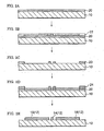
- the Schottky contacts 12 are lent an appropriately multilayer structure, in which case the material for each layer is selected from the abovementioned materials. These Schottky contacts 12 are formed onto the wafer 10 by a lift-off process. A method of forming the Schottky contacts 12 onto the wafer 10 will be explained while reference is made to Fig. 2.
- a negative resist 20 which is a photosensitive resin, is coated onto the entire surface of the wafer 10; (see Fig. 2A).
- a quartz mask 22 that has been patterned (stippled areas in the figure) with chrome into the form of the Schottky contacts described above is then laid onto the coated resist 20, and the wafer 10 and the quartz mask 22 are brought into contact; (see Fig. 2B) and exposed to ultraviolet rays with a mercury lamp (not illustrated) from above the quartz mask 22.
- a mercury lamp not illustrated
- the quartz mask 22 is removed and at the same time, the wafer 10 is developed, transferring onto it a pattern that is the reverse of the pattern on the quartz mask 22; (see Fig. 2C).
- an Au layer 24 is built by EB vapor deposition; (see Fig. 2D).
- Schottky contacts 12 of the desired shape are formed; (see Fig. 2E).
- Schottky contacts 12 are formed on the surface of the wafer 10 by putting it through a Schottky-contact 12 fabrication process (photolithography operations) such as in the foregoing. What is particularly significant here is that etching is not carried out on the wafer 10 surface in fabricating the Schottky contacts 12. The fact that an etching process, which would require a great deal of time, is thus not necessary serves to shorten the Schottky-contact 12 fabrication time.
- breakdown voltage in the present embodiment is, wherein a voltage at which a dc current flows from Schottky contact 18 to Schottky contact 14 has been applied, the voltage per 1 mm length of Schottky contact 14 at which a current of 1 mA flows between Schottky contact 14 and Schottky contact 18.
- breakdown voltage here signifies, in the working device (FET), "voltage per 1 mm gate width when a current of 1 mA flows between gate-drain.” Accordingly, if for example the length of Schottky contact 14 (gate width of the working device) is 100 ⁇ m, the voltage when a current of 10 -4 A flows between Schottky contact 14 (corresponding to the working-device gate) and Schottky contact 18 (corresponding to the working-device drain) would be the "breakdown voltage.”
- Schottky contact 18 is grounded, and meanwhile a dc circuit 26 for applying a negative voltage to Schottky contact 14 is formed. Then prior to measuring breakdown voltage, a constant current of 10 ⁇ A is applied for a 10-second interval. While it is known that flowing a current generally enhances breakdown voltage, in this way flowing a constant current in the circuit 26 to impart electrical stress from Schottky contact 18 to Schottky contact 14 stabilizes the breakdown voltage characteristics. The breakdown voltage is subsequently measured by flowing a dc current in the circuit 26.
- Fig. 4 then is a graph for a situation in which the voltage in the circuit 26 was increased gradually from 0 V.
- the horizontal axis in the graph is the value of the applied voltage, while the vertical axis is the value of the current flowing between Schottky contact 14 and Schottky contact 18.
- the current rose steeply until a voltage of about 2 V. Although the current thereafter ought to have saturated inasmuch as it was in the Schottky reverse direction, a definite saturation value could not be confirmed. This was an impairment to measuring the breakdown voltage with satisfactory accuracy.
- the breakdown voltage V 2 between Schottky contact 14 and Schottky contact 18 should satisfy relation (2) below.
- the FET breakdown voltage readily turns out to be the sought breakdown voltage V 1 or more.
- the breakdown-voltage measurement can be conducted with ease, because the breakdown voltage V 1 for a working device can be tested for even in cases in which large-sized contacts 12 are formed by the more convenient direct-contact optical exposure technique.
- the width of the first contact should be 0.8 ⁇ m or more, 5 ⁇ m or less; and the distance between the first contact and the second contact, and the distance between the first contact and the third contact should be 0.8 ⁇ m or more, 20 ⁇ m or less.
- the cleaning solution for clearing the oxide film from the wafer surface is not limited to hydrochloric acid, but as long as it removes oxide film, may be phosphoric acid, ammonia, sulfuric acid, aqueous hydrogen peroxide, or may be a solution containing a plurality of these liquids in a mixture.
- the wafer material is not limited to GaN, but may be expressed by whichever of: Al x Ga y In 1-x-y N (0 ⁇ x ⁇ 1, 0 ⁇ y ⁇ 1, x + y ⁇ 1); Al x G y In 1-x-y As (0 ⁇ x ⁇ 1, 0 ⁇ y ⁇ 1, x + y ⁇ 1); or Al x Ga y In 1-x-y P (0 ⁇ x ⁇ 1, 0 ⁇ y ⁇ 1, x + y ⁇ 1) ⁇ such as, for example, InP or AlGaN.
- Schottky contact 16 and Schottky contact 18 may have approximately the same positional relationship to Schottky contact 14, and either the one or the other Schottky contact 16 or Schottky contact 18 may be formed onto the wafer 10, because it will lead to the same results for the breakdown-voltage measurement.
- the applied voltage moreover, may be an ac voltage.
- the wafer 10 may be a structure in which the contact layer (an n-type GaAs layer for example) is left out from the epitaxial wafer structure for a GaAs-type high-electron mobility transistor.
- the contact layer an n-type GaAs layer for example
- a measurement that is substantially the same as the breakdown voltage measurement for the high-electron mobility transistor can be made.
- a measurement-facilitating method of measuring the breakdown voltage of a semiconductor epitaxial wafer, and a semiconductor epitaxial wafer whose breakdown voltage is superior are realized.
Abstract
A measurement-facilitating method of measuring the breakdown voltage
of a semiconductor epitaxial wafer, and a semiconductor epitaxial wafer whose
breakdown voltage is superior are realized.
In a method of measuring the breakdown voltage of a semiconductor
epitaxial wafer having to do with the present invention, the breakdown voltage
between contacts 12, 12 is measured only through the Schottky contacts,
without need for ohmic contacts. Inasmuch as the manufacturing process of
forming ohmic contacts is accordingly omitted, the semiconductor epitaxial
wafer 10 may be readily used in a breakdown-voltage measurement test. The
measurement of the wafer-10 breakdown voltage thus may be readily carried
out. Likewise, because the inter-contact breakdown voltage V2 of a wafer 10 can
be measured prior to manufacturing a working device from it, unsuitable
wafers 10 can be excluded before they are cycled through the working-device
fabrication process. Reduction in losses can accordingly be counted upon, in
contrast to conventional measuring methods, by which inter-contact breakdown
voltage V2 is measured following fabrication of the working devices.
Description
The present invention relates to semiconductor epitaxial wafers, and to
methods of measuring the breakdown voltage of semiconductor epitaxial
wafers.
Recently, even higher output from power FETs (field-effect transistors)
that are employed in base stations for mobile communications and in satellite
communications has been sought. While one way to realize higher power output
from an FET is to raise the operating voltage that is applied to it, owing to the
fact that the operating voltage is limited by the gate-to-drain breakdown
voltage (BV gd) of the FET, measuring the BV gd is a must. Here, "gate-to-drain
breakdown voltage" is for example a voltage value defined as, "voltage at which
a current of 1 mA per 1 mm gate width flows between gate-drain when a
reverse voltage is applied across the two terminals." Then to date, an
appropriate film has been built on a wafer as a substrate; the working device
including a Schottky contact (gate) and ohmic contacts (source, drain) has been
fabricated; and voltage has been applied across the Schottky contact-ohmic
contact.
Nonetheless, with methods of measuring the breakdown voltage of the
conventional epitaxial semiconductor wafer just described, issues such as the
following have persisted. In particular, if after fabricating a working device onto
a wafer the wafer is determined not to be up to standard for carrying out the
breakdown-voltage measurement, a great deal of time and expense ends up
being lost. Moreover, even cases in which the breakdown-voltage measurement
is carried out using a readily-fabricated "large device" (a device, larger than a
working device, from which measurements are taken), there has been a
problem in that with at least two patterning cycles being necessary―patterning
for the Schottky contact serving as the gate, and patterning for the ohmic
contacts serving as the source/drain―the fabricating process ends up costing a
great deal of time and trouble.
An object of the present invention, brought about in order to resolve the
foregoing issues, is thus to realize a measurement-facilitating method of
measuring the breakdown voltage of a semiconductor epitaxial wafer, and to
realize a semiconductor epitaxial wafer whose breakdown voltage is superior.
A method, involving the present invention, of measuring the breakdown
voltage of a semiconductor epitaxial wafer is characterized in that a voltage is
applied to a least one pair among a plurality of Schottky contacts formed onto a
semiconductor epitaxial wafer and the breakdown voltage across the contacts is
measured.
With this method of measuring the breakdown voltage of a
semiconductor epitaxial wafer inter-contact breakdown voltage is measured
with Schottky contacts only, ohmic contacts being unnecessary. The fact that
the manufacturing step of forming ohmic contacts is consequently omitted
enables providing for facilitated testing measurement of the breakdown voltage
of semiconductor epitaxial wafers. Semiconductor epitaxial wafer breakdown-voltage
measurement accordingly may be performed with ease. What is more,
because inter-contact breakdown voltage is measured prior to fabricating
working devices from wafer, a wafer that does not meet product specification
can be excluded before being passed onto working-device fabrication steps. This
consequently enables counting on reduction in time and expense losses
compared with conventional measuring methods by which inter-contact
breakdown voltage is measured after working devices are fabricated.
The surface of the semiconductor epitaxial wafer when the Schottky
contacts are to be formed is preferably flat. In forming the Schottky contacts,
because a step in which the wafer surface is etched is in this case unnecessary,
the time required to produce the contacts can be curtailed.
Likewise, the Schottky contacts are preferably formed onto the same
surface. Forming the Schottky contacts using a photolithographic process is in
that case facilitated.
The material for the Schottky contacts preferably contains one selected
from the group consisting of Au, Pt, Pd, W, Ti, Al and Ni. Thus selecting a
material suited to Schottky contacts enables more accurate breakdown-voltage
measurement to be carried out.
Before voltage is applied to the contacts, the semiconductor epitaxial
wafer surface is preferably cleaned with a cleaning solution containing at least
one of: hydrochloric acid, phosphoric acid, ammonia, sulfuric acid, and aqueous
hydrogen peroxide. The fact that contamination such as oxide film that forms
on the semiconductor epitaxial wafer can in that case be eliminated means that
leak current can be suppressed, and that more accurate inter-contact
breakdown voltage measurement can be made.
In addition, the structure of the semiconductor epitaxial wafer is
preferably one in which the contact layer has been removed from the epitaxial
structure for high electron mobility transistors. Measurement substantially
equivalent to measuring the breakdown voltage of high election mobility
transistors as working devices can in that case be made.
Preferable also is that the material for the semiconductor epitaxial wafer
be a compound expressed by: AlxGayIn1-x-yN (0 ≤ x ≤ 1, 0 ≤ y ≤ 1, x + y ≤ 1);
AlxGayIn1-x-yAs (0 ≤ x ≤ 1, 0 ≤ y ≤ 1, x + y ≤ 1); or AlxGayIn1-x-yP (0 ≤ x ≤ 1, 0 ≤ y ≤ 1,
x + y ≤ 1).
It is also preferable that as the Schottky contacts a first contact, a second
contact and a third contact, corresponding respectively to a working-device gate,
source and drain are formed onto the semiconductor epitaxial wafer. The first
contact, second contact and third contact can in that case be assumed to be the
gate, source and drain of a working device, whereby the breakdown voltage can
be measured with for example the source-to-drain distance, the gate length, etc.
put into desired conditions.
Preferable also is that angled portions of the second contact and third
contact where they oppose each other have a curved form. Inasmuch as arc
discharge arising between the neighboring second contact and third contact can
in that case be suppressed, more accurate breakdown-voltage measurement can
be carried out.
Preferably, the width of the first contact is 0.8 µm or more, 5 µm or less,
and the distance between the first contact and the second contact, and the
distance between the first contact and the third contact, is 0.8 µm or more, 20
µm or less. In this way, in cases in which the contacts are large-sized, Schottky
contacts can easily be fabricated by direct-contact optical exposure.
Furthermore, a constant current is preferably applied between the first
contact and the second contact before voltage is applied across them.
Stabilization of the breakdown voltage characteristics between the first contact
and the second contact by so-called electrical stress is in that case effected.
A semiconductor epitaxial wafer having to do with the present invention
is utilized as a substrate for FETs in which the gate-to-drain distance is L1 and
for which a breakdown voltage V1 between the gate and the drain is sought,
wherein the semiconductor epitaxial wafer is characterized in that given that
the distance between the first contact and the second contact is L2, the
breakdown voltage V2 between the first contact and the second contact,
measured by the foregoing breakdown-voltage-measurement method satisfies
the following relation.
V2 ≥ V1 × L2 /L1
With this semiconductor epitaxial wafer, because the breakdown voltage
V2 between the first contact and the second contact satisfies relation (1), the
breakdown voltage of a working device (FET) fabricated from such a wafer
readily turns out to be the sought breakdown voltage V1 or more. Wafers whose
breakdown voltage is superior can consequently be obtained.
With reference to the attached drawings a method, having to do with the
present invention in a most preferred embodiment, of measuring the
breakdown voltage of a semiconductor epitaxial wafer will be described below in
detail. Fig. 1 is a plan view representing a semiconductor epitaxial wafer used
for breakdown-voltage measurement.
As shown in Fig. 1 three Schottky contacts 12 are formed onto the
semiconductor epitaxial wafer (referred to simply as "wafer" hereinafter) 10.
With its uppermost layer (cap layer) being an n-type GaN epitaxial layer the
wafer 10 is fabricated by a suitably chosen semiconductor manufacturing
process to have a working-device field-effect transistor (FET). The topside of the
wafer 10 is approximately planar, and the Schottky contacts 12 are formed on
this same surface. (The Schottky contacts 12 are formed onto the wafer 10 by a
method that will be described later.)
The Schottky contacts 12 assume forms corresponding to the gate, source
and drain of the FET that is the working device. In particular, Schottky contact
14 (first contact) has a form corresponding to the gate, while Schottky contact
16 (second contact) and Schottky contact 18 (third contact) have forms
corresponding respectively to the source and drain.
Schottky contact 14 corresponding to the gate is configured with two
separated square contact portions 14a, and a rectilinear contact portion 14b
that interconnects the square contact portions 14a, 14a. The width of the
rectilinear contact portion 14b (corresponding to the FET gate length; length in
the side-to-side direction in the figure) is 1 µm; likewise the length of the
rectilinear contact portion 14b (corresponding to the FET gate width; length in
the up-and-down direction in the figure) is 100 µm. Schottky contact 16 and
Schottky contact 18 corresponding respectively to the source and drain are in
opposition flanking the rectilinear contact portion 14b of Schottky contact 14,
and have an approximately rectangular form in which the long edges parallel
the lengthwise direction of the Schottky contact 14. In particular, Schottky
contact 16 and Schottky contact 18 are approximately symmetrical with respect
to the rectilinear contact portion 14b of Schottky contact 14.
Among the comers of Schottky contact 16 and Schottky contact 18, those
on the sides where the like contacts 16, 18 oppose each other are given a smooth
curved contour, and the lateral surface of the corners is approximately the same
as the curved face of a circular cylindrical surface. Thus contouring the corners
of Schottky contact 16 and Schottky contact 18―in contrast to the situation in
which the corners are right angles―provides for suppressing the occurrence of
arc discharge arising between the contacts 16, 18. In addition, that fact that the
Schottky contacts 12 are formed so as to correspond to the gate, source and
drain of a working device means that the breakdown voltage measured will be a
value close to the inter-contact breakdown voltage of a working device.
The three Schottky contacts 12 are, moreover, constituted from Au. It
should be understood that other than Au, whichever of Pt, Pd, W, Ti, Al or Ni
can be selected as a material for the Schottky contacts, which likewise may be
an alloy that includes whichever of Pt, Pd, W, Ti, Al or Ni. Thus selecting a
material suited to the Schottky contacts 12 provides for performing the later-described
breakdown-voltage measurement the more accurately. The Schottky
contacts 12 are lent an appropriately multilayer structure, in which case the
material for each layer is selected from the abovementioned materials. These
Schottky contacts 12 are formed onto the wafer 10 by a lift-off process. A method
of forming the Schottky contacts 12 onto the wafer 10 will be explained while
reference is made to Fig. 2.
Initially a negative resist 20, which is a photosensitive resin, is coated
onto the entire surface of the wafer 10; (see Fig. 2A). A quartz mask 22 that has
been patterned (stippled areas in the figure) with chrome into the form of the
Schottky contacts described above is then laid onto the coated resist 20, and the
wafer 10 and the quartz mask 22 are brought into contact; (see Fig. 2B) and
exposed to ultraviolet rays with a mercury lamp (not illustrated) from above the
quartz mask 22. By bringing into contact and optically exposing the wafer 10
and the quartz mask 22 in this way―by adopting the so-called contact exposure
technique―the wafer 10 can be exposed with facility. The portions of the resist
20 that have been exposed thereby become insoluble. Subsequently the quartz
mask 22 is removed and at the same time, the wafer 10 is developed,
transferring onto it a pattern that is the reverse of the pattern on the quartz
mask 22; (see Fig. 2C). On the wafer 10 that has been formed in this way―that
has been formed with the reverse-patterned resist 20―an Au layer 24 is built
by EB vapor deposition; (see Fig. 2D). Then lastly, by removing the resist 20 and
the Au layer built on the resist 20 (the so-called lift-off process), Schottky
contacts 12 of the desired shape are formed; (see Fig. 2E).
A method of measuring the breakdown voltage of Schottky contacts 12
formed in the foregoing manner will next be explained. Here, "breakdown
voltage" in the present embodiment is, wherein a voltage at which a dc current
flows from Schottky contact 18 to Schottky contact 14 has been applied, the
voltage per 1 mm length of Schottky contact 14 at which a current of 1 mA flows
between Schottky contact 14 and Schottky contact 18. That is, breakdown
voltage here signifies, in the working device (FET), "voltage per 1 mm gate
width when a current of 1 mA flows between gate-drain." Accordingly, if for
example the length of Schottky contact 14 (gate width of the working device) is
100 µm, the voltage when a current of 10-4 A flows between Schottky contact 14
(corresponding to the working-device gate) and Schottky contact 18
(corresponding to the working-device drain) would be the "breakdown voltage."
As illustrated in Fig. 3, Schottky contact 18 is grounded, and meanwhile
a dc circuit 26 for applying a negative voltage to Schottky contact 14 is formed.
Then prior to measuring breakdown voltage, a constant current of 10 µA is
applied for a 10-second interval. While it is known that flowing a current
generally enhances breakdown voltage, in this way flowing a constant current
in the circuit 26 to impart electrical stress from Schottky contact 18 to Schottky
contact 14 stabilizes the breakdown voltage characteristics. The breakdown
voltage is subsequently measured by flowing a dc current in the circuit 26.
Inasmuch as in this situation the current flowing from the Schottky
contact 18 to the wafer 10 is in the Schottky-contact forward direction in which
the contact resistance is small, the current flows smoothly. Particularly
significant is that Schottky contact 18, corresponding to the drain of a working
device, functions as does an ohmic contact. This means that measurement of
Schottky-contact 14 breakdown voltage is made without forming ohmic contacts
onto the wafer 10. Accordingly, the wafer 10 having the contacts 12 can be
readily fabricated, in contrast to the case with breakdown-voltage
measurement techniques to date, which have dictated that ohmic contacts be
formed onto the wafer 10.
Fig. 4 then is a graph for a situation in which the voltage in the circuit 26
was increased gradually from 0 V. The horizontal axis in the graph is the value
of the applied voltage, while the vertical axis is the value of the current flowing
between Schottky contact 14 and Schottky contact 18. As is clear from the
graph, the current rose steeply until a voltage of about 2 V. Although the
current thereafter ought to have saturated inasmuch as it was in the Schottky
reverse direction, a definite saturation value could not be confirmed. This was
an impairment to measuring the breakdown voltage with satisfactory accuracy.
Given the circumstances, the inventors discovered after concerted investigation
that not being able to confirm a clear saturation in the current value was due to
leakage current, and that what turned out to be the causative factor behind the
leakage current, oxide film on the wafer surface between the contacts 12, should
be cleared with hydrochloric acid.
Accordingly, after eliminating with hydrochloric acid the oxide film on
the wafer surface between the contacts 12, the measurement was made once
more. A graph of the results of this measurement is plotted in Fig. 5. The
horizontal and vertical axes are the same as in Fig. 4. As is clear from this
graph, the current does manifest a definite saturation value, and the puncture
voltage is 32 V or so. Then from reading the voltage (breakdown voltage) for
when a current of 10-4 A―because the length of Schottky contact 14 is 100
µm―flows between Schottky contact 14 and Schottky contact 18, it is evident
that value is 38 V or so. Measurement of the breakdown voltage is in this way
finished.
Subjecting the wafer 10 on which the contacts 12 are formed to the
breakdown-voltage measurement test as explained in detail in the foregoing
measures the breakdown voltage between the contacts 14 and 18 through
Schottky contacts only, without need for ohmic contacts. The fact that the
manufacturing process of forming ohmic contacts is accordingly omitted enables
the contacts 12 to be created through only a single-cycle photolithography
process. Inasmuch as the wafer 10 may thereby be readily used in the
breakdown-voltage measurement test, the measurement of the wafer 10
breakdown voltage may be readily carried out. By the same token, because the
inter-contact breakdown voltage of a wafer 10 can be measured prior to
manufacturing a working device from it, unsuitable wafers 10 can be excluded
before they are cycled through the working-device fabrication process.
Reduction in losses can accordingly be counted upon, in contrast to conventional
measuring methods, by which inter-contact breakdown voltage is measured
following fabrication of the working devices.
At this point, a technique of measuring breakdown voltage by means of
contacts that are larger-sized than the size desired in a FET will be explained.
The fact that in general breakdown voltage of a working device is
approximately inversely proportional to the distance over the gate-drain
interval is known. Consequently, wherein the gate-drain distance in and
breakdown voltage desired in an FET are L1 and V1, the distance L2 (referring to
Fig. 3), and the breakdown voltage V2, between Schottky contact 14 and
Schottky contact 18 on a wafer 10 subjected to breakdown-voltage
measurement may be expressed by the following relational formula.
V2 /L2 ≒ V1 /L1
Therefore, in order that the desired FET breakdown voltage satisfy at
least V1, the breakdown voltage V2 between Schottky contact 14 and Schottky
contact 18 should satisfy relation (2) below.
V2 ≥ V1 × L2 /L1
By the breakdown voltage V2 then satisfying relation (2), the FET
breakdown voltage readily turns out to be the sought breakdown voltage V1 or
more. This means that the breakdown-voltage measurement can be conducted
with ease, because the breakdown voltage V1 for a working device can be tested
for even in cases in which large-sized contacts 12 are formed by the more
convenient direct-contact optical exposure technique. As far as dimensions that
facilitate fabrication by the contact-exposure technique are concerned, the
width of the first contact should be 0.8 µm or more, 5 µm or less; and the
distance between the first contact and the second contact, and the distance
between the first contact and the third contact should be 0.8 µm or more, 20 µm
or less.
The present invention is not limited to the embodiment described above,
in that various modifications are possible. For example, the cleaning solution
for clearing the oxide film from the wafer surface is not limited to hydrochloric
acid, but as long as it removes oxide film, may be phosphoric acid, ammonia,
sulfuric acid, aqueous hydrogen peroxide, or may be a solution containing a
plurality of these liquids in a mixture. Likewise, the wafer material is not
limited to GaN, but may be expressed by whichever of: AlxGayIn1-x-yN (0 ≤ x ≤ 1,
0 ≤ y ≤ 1, x + y ≤ 1); AlxGyIn1-x-yAs (0 ≤ x ≤ 1, 0 ≤ y ≤ 1, x + y ≤ 1); or AlxGayIn1-x-yP
(0 ≤ x ≤ 1, 0 ≤ y ≤ 1, x + y ≤ 1)―such as, for example, InP or AlGaN.
Furthermore, Schottky contact 16 and Schottky contact 18 may have
approximately the same positional relationship to Schottky contact 14, and
either the one or the other Schottky contact 16 or Schottky contact 18 may be
formed onto the wafer 10, because it will lead to the same results for the
breakdown-voltage measurement. The applied voltage, moreover, may be an ac
voltage.
In addition, the wafer 10 may be a structure in which the contact layer
(an n-type GaAs layer for example) is left out from the epitaxial wafer structure
for a GaAs-type high-electron mobility transistor. In this case, prior to
fabricating the high-electron mobility transistor as a working device, a
measurement that is substantially the same as the breakdown voltage
measurement for the high-electron mobility transistor can be made.
In terms of the present invention, a measurement-facilitating method of
measuring the breakdown voltage of a semiconductor epitaxial wafer, and a
semiconductor epitaxial wafer whose breakdown voltage is superior are
realized.
Claims (12)
- A method of measuring said breakdown voltage of a semiconductor epitaxial wafer, characterized in that: a voltage is applied to a least one pair of contacts among a plurality of Schottky contacts formed onto a semiconductor epitaxial wafer, and said breakdown voltage across said contacts is measured.
- A semiconductor epitaxial wafer breakdown-voltage measurement method as set forth in claim 1, characterized in that in forming said Schottky contacts said semiconductor epitaxial wafer is superficially flat.
- A semiconductor epitaxial wafer breakdown-voltage measurement method as set forth in claim 2, characterized in that said Schottky contacts are formed onto said same surface.
- A semiconductor epitaxial wafer breakdown-voltage measurement method as set forth in any one of claims 1 through 3, characterized in that said Schottky contact materially contains one selected from said group consisting of Au, Pt, Pd, W, Ti, Al and Ni.
- A semiconductor epitaxial wafer breakdown-voltage measurement method as set forth in any one of claims 1 through 4, characterized in that before said voltage application, said semiconductor epitaxial wafer is superficially cleaned with a cleaning solution containing at least one of: hydrochloric acid, phosphoric acid, ammonia, sulfuric acid, and hydrogen p eroxide.
- A semiconductor epitaxial wafer breakdown-voltage measurement method as set forth in any one of claims 1 through 5, characterized in that said structure of said semiconductor epitaxial wafer is one in which said contact layer has been removed from a high-electron-mobility-transistor epitaxial structure.
- A semiconductor epitaxial wafer breakdown-voltage measurement method as set forth in any one of claims 1 through 6, characterized in that said semiconductor epitaxial wafer materially is a compound expressed by: AlxGayIn1-x-yN (0 ≤ x ≤ 1, 0 ≤ y ≤ 1, x + y ≤ 1); AlxGayIn1-x-yAs (0 ≤ x ≤ 1, 0 ≤ y ≤ 1, x + y ≤ 1); or AlxGayIn1-x-yP (0 ≤ x ≤ 1, 0 ≤ y ≤ 1, x + y ≤ 1).
- A semiconductor epitaxial wafer breakdown-voltage measurement method as set forth in any one of claims 1 through 7, characterized in that as said Schottky contacts a first contact, a second contact and a third contact, corresponding respectively to a working-device gate, source and drain are formed onto said semiconductor epitaxial wafer.
- A semiconductor epitaxial wafer breakdown-voltage measurement method as set forth in claim 8, characterized in that angled portions of said second contact and third contact where they oppose each other have a curved form.
- A semiconductor epitaxial wafer breakdown-voltage measurement method as set forth in claim 8 or 9, characterized in that said first contact is 0.8 µm or more, 5 µm or less in width; and distance separating said first contact and said second contact, and said distance separating said first contact and said third contact, is 0.8 µm or more, 20 µm or less.
- A semiconductor epitaxial wafer breakdown-voltage measurement method as set forth in any one of claims 8 through 10, characterized in that a constant current is applied between said first contact and said second contact before said voltage application.
- A semiconductor epitaxial wafer utilized as a substrate for FETs in which said gate-to-drain distance is L1 and for which a breakdown voltage V1 between said gate and said drain is sought, said semiconductor epitaxial wafer' characterized in that:wherein said distance separating said first contact and said second contact is L2, said breakdown voltage V2 between said first contact and said second contact, measured by said breakdown-voltage-measurement method set forth in claim 8 satisfies said following relation (1)
Applications Claiming Priority (3)
| Application Number | Priority Date | Filing Date | Title |
|---|---|---|---|
| JP2002128681A JP4126953B2 (en) | 2002-04-30 | 2002-04-30 | Method for measuring pressure resistance of semiconductor epitaxial wafer |
| JP2002128681 | 2002-04-30 | ||
| PCT/JP2003/000612 WO2003094223A1 (en) | 2002-04-30 | 2003-01-23 | Method for measuring withstand voltage of semiconductor epitaxial wafer and semiconductor epitaxial wafer |
Publications (2)
| Publication Number | Publication Date |
|---|---|
| EP1503408A1 true EP1503408A1 (en) | 2005-02-02 |
| EP1503408A4 EP1503408A4 (en) | 2009-08-12 |
Family
ID=29397272
Family Applications (1)
| Application Number | Title | Priority Date | Filing Date |
|---|---|---|---|
| EP03703038A Withdrawn EP1503408A4 (en) | 2002-04-30 | 2003-01-23 | Method for measuring withstand voltage of semiconductor epitaxial wafer and semiconductor epitaxial wafer |
Country Status (7)
| Country | Link |
|---|---|
| US (1) | US7195937B2 (en) |
| EP (1) | EP1503408A4 (en) |
| JP (1) | JP4126953B2 (en) |
| KR (1) | KR100955368B1 (en) |
| CN (1) | CN1295772C (en) |
| TW (1) | TW200400582A (en) |
| WO (1) | WO2003094223A1 (en) |
Families Citing this family (6)
| Publication number | Priority date | Publication date | Assignee | Title |
|---|---|---|---|---|
| JPH0720339U (en) * | 1993-05-12 | 1995-04-11 | 日本鋪道株式会社 | Generated soil treatment device |
| CN101388353B (en) * | 2007-09-10 | 2010-05-19 | 中芯国际集成电路制造(上海)有限公司 | Method for monitoring stability of water breakdown voltage |
| JP2010272577A (en) * | 2009-05-19 | 2010-12-02 | Takehisa Sasaki | Radiation detecting element and radiation detector |
| CN103364694B (en) * | 2012-03-26 | 2016-06-01 | 上海华虹宏力半导体制造有限公司 | The device and method that the drain-source breakdown voltage of super measurement source table scope is measured |
| CN103389443B (en) * | 2012-05-07 | 2015-12-09 | 无锡华润上华科技有限公司 | The method of testing of dynamic breakdown voltage of silicon on insulator MOS device |
| JP5913272B2 (en) * | 2013-12-11 | 2016-04-27 | 誉田 雄久 | Radiation detection element and radiation detection apparatus |
Citations (3)
| Publication number | Priority date | Publication date | Assignee | Title |
|---|---|---|---|---|
| JPS54131880A (en) * | 1978-04-03 | 1979-10-13 | Nec Corp | Manufacture of schottky junction element |
| JPH03166745A (en) * | 1989-11-27 | 1991-07-18 | Nippon Mining Co Ltd | Evaluating method for field effect transistor |
| JPH06232177A (en) * | 1993-02-05 | 1994-08-19 | Sumitomo Electric Ind Ltd | Field effect transistor and its manufacture |
Family Cites Families (6)
| Publication number | Priority date | Publication date | Assignee | Title |
|---|---|---|---|---|
| JP2520870B2 (en) * | 1985-08-13 | 1996-07-31 | 沖電気工業株式会社 | Method for manufacturing semiconductor device |
| JP3206621B2 (en) * | 1993-07-28 | 2001-09-10 | 住友電気工業株式会社 | Field effect transistor |
| US5535231A (en) * | 1994-11-08 | 1996-07-09 | Samsung Electronics Co., Ltd. | Optoelectronic circuit including heterojunction bipolar transistor laser and photodetector |
| JP3156620B2 (en) * | 1997-02-12 | 2001-04-16 | 日本電気株式会社 | Field effect transistor and method of manufacturing the same |
| JP3127874B2 (en) * | 1998-02-12 | 2001-01-29 | 日本電気株式会社 | Field effect transistor and method of manufacturing the same |
| US6177322B1 (en) * | 1998-10-23 | 2001-01-23 | Advanced Mictro Devices, Inc. | High voltage transistor with high gated diode breakdown voltage |
-
2002
- 2002-04-30 JP JP2002128681A patent/JP4126953B2/en not_active Expired - Fee Related
-
2003
- 2003-01-23 KR KR1020047000447A patent/KR100955368B1/en not_active IP Right Cessation
- 2003-01-23 US US10/484,001 patent/US7195937B2/en not_active Expired - Fee Related
- 2003-01-23 CN CNB038006278A patent/CN1295772C/en not_active Expired - Fee Related
- 2003-01-23 WO PCT/JP2003/000612 patent/WO2003094223A1/en active Application Filing
- 2003-01-23 EP EP03703038A patent/EP1503408A4/en not_active Withdrawn
- 2003-04-15 TW TW092108656A patent/TW200400582A/en not_active IP Right Cessation
Patent Citations (3)
| Publication number | Priority date | Publication date | Assignee | Title |
|---|---|---|---|---|
| JPS54131880A (en) * | 1978-04-03 | 1979-10-13 | Nec Corp | Manufacture of schottky junction element |
| JPH03166745A (en) * | 1989-11-27 | 1991-07-18 | Nippon Mining Co Ltd | Evaluating method for field effect transistor |
| JPH06232177A (en) * | 1993-02-05 | 1994-08-19 | Sumitomo Electric Ind Ltd | Field effect transistor and its manufacture |
Non-Patent Citations (1)
| Title |
|---|
| See also references of WO03094223A1 * |
Also Published As
| Publication number | Publication date |
|---|---|
| JP4126953B2 (en) | 2008-07-30 |
| EP1503408A4 (en) | 2009-08-12 |
| US20050118736A1 (en) | 2005-06-02 |
| KR100955368B1 (en) | 2010-04-29 |
| KR20040101987A (en) | 2004-12-03 |
| TW200400582A (en) | 2004-01-01 |
| US7195937B2 (en) | 2007-03-27 |
| CN1295772C (en) | 2007-01-17 |
| CN1547767A (en) | 2004-11-17 |
| WO2003094223A1 (en) | 2003-11-13 |
| TWI316277B (en) | 2009-10-21 |
| JP2003324137A (en) | 2003-11-14 |
Similar Documents
| Publication | Publication Date | Title |
|---|---|---|
| JP3884047B2 (en) | Method for manufacturing field effect transistor | |
| US7195937B2 (en) | Method for measuring withstand voltage of semiconductor epitaxial wafer and semiconductor epitaxial wafer | |
| EP0718877A2 (en) | Method of manufacturing a MESFET | |
| US11616129B2 (en) | Contact photolithography-based nanopatterning using photoresist features having re-entrant profiles | |
| Uchida et al. | Short-channel a-Si thin-film MOS transistors | |
| CN109727918B (en) | Structure of integrated enhancement mode and depletion mode field effect transistor and manufacturing method thereof | |
| KR101064726B1 (en) | Semiconductor device and method of fabrricating the same | |
| EP0385031B1 (en) | Semiconductor device with a recessed gate, and a production method thereof | |
| KR101104251B1 (en) | Method of fabrricating semiconductor device | |
| KR101042709B1 (en) | Method of fabrricating semiconductor device | |
| KR100849926B1 (en) | Methods for fabricating a pseudomorphic high electron mobility transistor | |
| JPH07130766A (en) | Compound semiconductor device | |
| KR100236662B1 (en) | Photoetching method of an ingap layer | |
| KR100315423B1 (en) | Method of forming fine T(Γ)-gate by photo-lithography process and sacrificial dielectric film | |
| US20090233414A1 (en) | Method for fabricating group III-nitride high electron mobility transistors (HEMTs) | |
| JP3107681B2 (en) | Etching control method for recess structure FET | |
| Li | Improving Gain and Efficiency of N-polar GaN Deep Recess HEMT for mm-Wave Applications | |
| KR101064727B1 (en) | Semiconductor device and method of fabrricating the same | |
| KR20000002537A (en) | Transistor forming method for testing in chemical semiconductor device. | |
| JPH02273939A (en) | Manufacture of field effect type semiconductor device | |
| KR20060028315A (en) | Gate with wide head and method for producing the same | |
| JPS6396961A (en) | Manufacture of field-effect transistor | |
| Hersener et al. | A MOSFET, manufactured with synchrotron X-ray lithography | |
| JPH07302885A (en) | Field effect transistor | |
| Schuette | Advanced processing for scaled depletion and enhancement-mode AlGaN/GaN HEMTs |
Legal Events
| Date | Code | Title | Description |
|---|---|---|---|
| PUAI | Public reference made under article 153(3) epc to a published international application that has entered the european phase |
Free format text: ORIGINAL CODE: 0009012 |
|
| 17P | Request for examination filed |
Effective date: 20040115 |
|
| AK | Designated contracting states |
Kind code of ref document: A1 Designated state(s): AT BE BG CH CY CZ DE DK EE ES FI FR GB GR HU IE IT LI LU MC NL PT SE SI SK TR |
|
| A4 | Supplementary search report drawn up and despatched |
Effective date: 20090714 |
|
| 17Q | First examination report despatched |
Effective date: 20091211 |
|
| STAA | Information on the status of an ep patent application or granted ep patent |
Free format text: STATUS: THE APPLICATION IS DEEMED TO BE WITHDRAWN |
|
| 18D | Application deemed to be withdrawn |
Effective date: 20170704 |