EP1503362A2 - Device and method for driving a plasma display panel, and a plasma display device - Google Patents
Device and method for driving a plasma display panel, and a plasma display device Download PDFInfo
- Publication number
- EP1503362A2 EP1503362A2 EP04090298A EP04090298A EP1503362A2 EP 1503362 A2 EP1503362 A2 EP 1503362A2 EP 04090298 A EP04090298 A EP 04090298A EP 04090298 A EP04090298 A EP 04090298A EP 1503362 A2 EP1503362 A2 EP 1503362A2
- Authority
- EP
- European Patent Office
- Prior art keywords
- voltage
- electrode
- inductor
- energy
- panel capacitor
- Prior art date
- Legal status (The legal status is an assumption and is not a legal conclusion. Google has not performed a legal analysis and makes no representation as to the accuracy of the status listed.)
- Withdrawn
Links
Images








Classifications
-
- G—PHYSICS
- G09—EDUCATION; CRYPTOGRAPHY; DISPLAY; ADVERTISING; SEALS
- G09G—ARRANGEMENTS OR CIRCUITS FOR CONTROL OF INDICATING DEVICES USING STATIC MEANS TO PRESENT VARIABLE INFORMATION
- G09G3/00—Control arrangements or circuits, of interest only in connection with visual indicators other than cathode-ray tubes
- G09G3/20—Control arrangements or circuits, of interest only in connection with visual indicators other than cathode-ray tubes for presentation of an assembly of a number of characters, e.g. a page, by composing the assembly by combination of individual elements arranged in a matrix no fixed position being assigned to or needed to be assigned to the individual characters or partial characters
- G09G3/22—Control arrangements or circuits, of interest only in connection with visual indicators other than cathode-ray tubes for presentation of an assembly of a number of characters, e.g. a page, by composing the assembly by combination of individual elements arranged in a matrix no fixed position being assigned to or needed to be assigned to the individual characters or partial characters using controlled light sources
- G09G3/28—Control arrangements or circuits, of interest only in connection with visual indicators other than cathode-ray tubes for presentation of an assembly of a number of characters, e.g. a page, by composing the assembly by combination of individual elements arranged in a matrix no fixed position being assigned to or needed to be assigned to the individual characters or partial characters using controlled light sources using luminous gas-discharge panels, e.g. plasma panels
- G09G3/288—Control arrangements or circuits, of interest only in connection with visual indicators other than cathode-ray tubes for presentation of an assembly of a number of characters, e.g. a page, by composing the assembly by combination of individual elements arranged in a matrix no fixed position being assigned to or needed to be assigned to the individual characters or partial characters using controlled light sources using luminous gas-discharge panels, e.g. plasma panels using AC panels
- G09G3/296—Driving circuits for producing the waveforms applied to the driving electrodes
-
- G—PHYSICS
- G09—EDUCATION; CRYPTOGRAPHY; DISPLAY; ADVERTISING; SEALS
- G09G—ARRANGEMENTS OR CIRCUITS FOR CONTROL OF INDICATING DEVICES USING STATIC MEANS TO PRESENT VARIABLE INFORMATION
- G09G3/00—Control arrangements or circuits, of interest only in connection with visual indicators other than cathode-ray tubes
- G09G3/20—Control arrangements or circuits, of interest only in connection with visual indicators other than cathode-ray tubes for presentation of an assembly of a number of characters, e.g. a page, by composing the assembly by combination of individual elements arranged in a matrix no fixed position being assigned to or needed to be assigned to the individual characters or partial characters
- G09G3/22—Control arrangements or circuits, of interest only in connection with visual indicators other than cathode-ray tubes for presentation of an assembly of a number of characters, e.g. a page, by composing the assembly by combination of individual elements arranged in a matrix no fixed position being assigned to or needed to be assigned to the individual characters or partial characters using controlled light sources
- G09G3/28—Control arrangements or circuits, of interest only in connection with visual indicators other than cathode-ray tubes for presentation of an assembly of a number of characters, e.g. a page, by composing the assembly by combination of individual elements arranged in a matrix no fixed position being assigned to or needed to be assigned to the individual characters or partial characters using controlled light sources using luminous gas-discharge panels, e.g. plasma panels
- G09G3/288—Control arrangements or circuits, of interest only in connection with visual indicators other than cathode-ray tubes for presentation of an assembly of a number of characters, e.g. a page, by composing the assembly by combination of individual elements arranged in a matrix no fixed position being assigned to or needed to be assigned to the individual characters or partial characters using controlled light sources using luminous gas-discharge panels, e.g. plasma panels using AC panels
- G09G3/296—Driving circuits for producing the waveforms applied to the driving electrodes
- G09G3/2965—Driving circuits for producing the waveforms applied to the driving electrodes using inductors for energy recovery
-
- G—PHYSICS
- G09—EDUCATION; CRYPTOGRAPHY; DISPLAY; ADVERTISING; SEALS
- G09G—ARRANGEMENTS OR CIRCUITS FOR CONTROL OF INDICATING DEVICES USING STATIC MEANS TO PRESENT VARIABLE INFORMATION
- G09G2310/00—Command of the display device
- G09G2310/06—Details of flat display driving waveforms
- G09G2310/066—Waveforms comprising a gently increasing or decreasing portion, e.g. ramp
-
- G—PHYSICS
- G09—EDUCATION; CRYPTOGRAPHY; DISPLAY; ADVERTISING; SEALS
- G09G—ARRANGEMENTS OR CIRCUITS FOR CONTROL OF INDICATING DEVICES USING STATIC MEANS TO PRESENT VARIABLE INFORMATION
- G09G2330/00—Aspects of power supply; Aspects of display protection and defect management
- G09G2330/02—Details of power systems and of start or stop of display operation
-
- G—PHYSICS
- G09—EDUCATION; CRYPTOGRAPHY; DISPLAY; ADVERTISING; SEALS
- G09G—ARRANGEMENTS OR CIRCUITS FOR CONTROL OF INDICATING DEVICES USING STATIC MEANS TO PRESENT VARIABLE INFORMATION
- G09G3/00—Control arrangements or circuits, of interest only in connection with visual indicators other than cathode-ray tubes
- G09G3/20—Control arrangements or circuits, of interest only in connection with visual indicators other than cathode-ray tubes for presentation of an assembly of a number of characters, e.g. a page, by composing the assembly by combination of individual elements arranged in a matrix no fixed position being assigned to or needed to be assigned to the individual characters or partial characters
- G09G3/22—Control arrangements or circuits, of interest only in connection with visual indicators other than cathode-ray tubes for presentation of an assembly of a number of characters, e.g. a page, by composing the assembly by combination of individual elements arranged in a matrix no fixed position being assigned to or needed to be assigned to the individual characters or partial characters using controlled light sources
- G09G3/28—Control arrangements or circuits, of interest only in connection with visual indicators other than cathode-ray tubes for presentation of an assembly of a number of characters, e.g. a page, by composing the assembly by combination of individual elements arranged in a matrix no fixed position being assigned to or needed to be assigned to the individual characters or partial characters using controlled light sources using luminous gas-discharge panels, e.g. plasma panels
- G09G3/288—Control arrangements or circuits, of interest only in connection with visual indicators other than cathode-ray tubes for presentation of an assembly of a number of characters, e.g. a page, by composing the assembly by combination of individual elements arranged in a matrix no fixed position being assigned to or needed to be assigned to the individual characters or partial characters using controlled light sources using luminous gas-discharge panels, e.g. plasma panels using AC panels
- G09G3/291—Control arrangements or circuits, of interest only in connection with visual indicators other than cathode-ray tubes for presentation of an assembly of a number of characters, e.g. a page, by composing the assembly by combination of individual elements arranged in a matrix no fixed position being assigned to or needed to be assigned to the individual characters or partial characters using controlled light sources using luminous gas-discharge panels, e.g. plasma panels using AC panels controlling the gas discharge to control a cell condition, e.g. by means of specific pulse shapes
- G09G3/294—Control arrangements or circuits, of interest only in connection with visual indicators other than cathode-ray tubes for presentation of an assembly of a number of characters, e.g. a page, by composing the assembly by combination of individual elements arranged in a matrix no fixed position being assigned to or needed to be assigned to the individual characters or partial characters using controlled light sources using luminous gas-discharge panels, e.g. plasma panels using AC panels controlling the gas discharge to control a cell condition, e.g. by means of specific pulse shapes for lighting or sustain discharge
Definitions
- the present invention relates to a device and method for driving a plasma display panel (PDP), and a plasma display device. More specifically, the present invention relates to an energy recovery circuit of the PDP.
- PDP plasma display panel
- a PDP is a flat panel display that uses plasma generated by gas discharge to display characters or images. It includes, depending on its size, more than several scores to millions of pixels arranged in a matrix pattern.
- a PDP is classified as a direct current (DC) type or an alternating current (AC) type according to its discharge cell structure and the waveform of the driving voltage applied thereto.
- the DC PDP has electrodes exposed to a discharge space to allow current to flow through the discharge space while the voltage is applied, and thus requires a resistance for limiting the current.
- the AC PDP has electrodes covered with a dielectric layer that forms a capacitor to limit the current and protect the electrodes from the impact of ions during discharge.
- the AC PDP has a longer lifetime than the DC PDP.
- FIG. 1 is a partial perspective view of an AC PDP.
- a plurality of pairs of scan electrodes 4 and sustain electrodes 5 are arranged in parallel and are covered with a dielectric layer 2 and a protective layer 3.
- a plurality of address electrodes 8 covered with an insulating layer 7 are arranged.
- Barrier ribs 9 are formed in parallel with the address electrodes 8 on the insulating layer 7, which is interposed between the address electrodes 8.
- a fluorescent material 10 is formed on the surface of the insulating layer 7 and on both sides of the barrier ribs 9.
- the first and second glass substrates 1 and 6 are arranged face-to-face with a discharge space 11 formed therebetween, and the scan electrodes 4 and the sustain electrodes 5 lie normal to the address electrodes 8.
- the discharge space at the intersection between the address electrode 8 and the pair of scan electrode 4 and sustain electrode 5 forms a discharge cell 12.
- FIG. 2 shows an arrangement of electrodes in the PDP.
- the PDP has a pixel matrix consisting of mxn discharge cells.
- address electrodes A 1 to A m are arranged in columns, and scan electrodes Y 1 to Y n and sustain electrodes X 1 to X n are alternately arranged in rows.
- Discharge cells 12 shown in FIG. 2 correspond to the discharge cells 12 in FIG. 1.
- the method for driving the AC PDP includes a reset period, an addressing period, a sustain period, and an erase period in temporal sequence.
- the reset period is for initiating the status of each cell so as to facilitate the addressing operation.
- the addressing period is for selecting turn-on/off cells and applying an address voltage to the turn-on cells (i.e., addressed cells) to accumulate wall charges.
- the sustain period is for applying sustain pulses and causing a sustain-discharge for displaying an image on the addressed cells.
- the erase period is for reducing the wall charges of the cells to terminate the sustain-discharge.
- the discharge spaces between the scan and sustain electrodes and between the address electrode side and the scan/sustain electrode side act as a capacitance load (hereinafter, referred to as "panel capacitor"), so capacitance exists on the panel. Due to the capacitance of the panel capacitor, reactive power is needed to apply a waveform for the sustain-discharge.
- the PDP driver circuit includes a power recovery circuit for recovering the reactive power and reusing it, some of said power recovery circuit having been elucidated by L.F. Weber in U.S. Patent Nos. 4,866,349 and 5,081,400.
- the circuit designed by Weber repeatedly transfers energy from the panel to a power recovery capacitor or energy from the power recovery capacitor to the panel using a resonance between the panel capacitor and an inductor, thus recovering the effective power.
- the rise/fall time of the panel voltage is dependent upon the time constant LC determined by the inductance L of the inductor and the capacitance C of the panel capacitor.
- the rise time of the panel voltage is equal to the fall time because LC is constant.
- the switch coupled to the power source must be hard-switched during the rise of the panel voltage, in which case stress on the switch increases.
- the hard-switching operation also causes a power loss and increases the effect of electromagnetic interference (EMI).
- EMI electromagnetic interference
- a device for driving a plasma display panel which has first and second electrodes with a panel capacitor formed therebetween, comprises:
- a charge/discharge unit comprising a first inductor coupled to the first electrode, the charge/discharge unit changing the voltage of the first electrode from a first voltage to a second voltage by using the first inductor;
- a sustain unit maintaining the voltage of the first electrode at the second voltage during a predetermined period after the voltage of the first electrode is changed to the second voltage
- the charge/discharge unit changes the voltage of the first electrode from the first voltage to a third voltage while increasing the magnitude of a current flowing in the first inductor, and changes the voltage of the first electrode from the third voltage to the second voltage while decreasing the magnitude of the current flowing in the first inductor;
- the third voltage is between a fourth voltage, corresponding to the mean value of the first and second voltages, and the second voltage.
- a method for driving a plasma display panel which has first and second electrodes with a panel capacitor formed therebetween, comprises:
- first voltage is between a third voltage, which corresponds to half of the second voltage, and the second voltage.
- a method for driving a plasma display panel which has first and second electrodes with a panel capacitor formed therebetween, comprises:
- the voltage of the first electrode is firstly changed from the first voltage to a third voltage while increasing the magnitude of a current flowing in the first inductor, and secondly changed from the third voltage to the second voltage while decreasing the magnitude of the current flowing in the first inductor, where the third voltage is between a fourth voltage, which corresponds to the mean value of the first and second voltages, and the second voltage.
- a method for driving a plasma display panel which has first and second electrodes with a panel capacitor formed therebetween, comprises:
- the voltage of the first electrode is firstly changed from the first voltage to a third voltage while increasing the magnitude of a current flowing in the first inductor, and secondly changed from the third voltage to the second voltage while decreasing the magnitude of the current flowing in the first inductor, where the third voltage is between a fourth voltage, which corresponds to the mean value of the first and second voltages, and the second voltage.
- a plasma display device comprises:
- a plasma display panel having first and second electrodes with a panel capacitor formed therebetween;
- a driving circuit comprising an inductor coupled to the first electrode, the driving circuit applying a driving voltage to the first electrode,
- the driving circuit firstly charges the panel capacitor to a voltage greater than half of a desired voltage while increasing the magnitude of a current flowing in the inductor, and secondly charges the panel capacitor to the desired voltage while decreasing the magnitude of the current flowing in the inductor.
- a plasma display device comprises:
- a plasma display panel having first and second electrodes with a panel capacitor formed therebetween;
- a driving circuit comprising first and second inductors coupled to the first electrode in parallel, the driving circuit applying a driving voltage to the first electrode,
- the driving circuit firstly charges the panel capacitor to a voltage greater than half of a desired voltage while increasing the magnitude of a current flowing in the first inductor, and secondly charges the panel capacitor to the desired voltage while decreasing the magnitude of the current flowing in the first inductor;
- the driving circuit discharges the panel capacitor by using the second inductor.
- FIG. 1 is a partial perspective view of an AC PDP.
- FIG. 2 shows an arrangement of electrodes in the AC PDP.
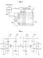
- FIG. 3 is a schematic block diagram of a plasma display device according to an embodiment of the present invention.
- FIG. 4 is a schematic circuit diagram of an energy recovery circuit according to a first embodiment of the present invention.
- FIG. 5 is a timing diagram of the energy recovery circuit according to the first embodiment of the present invention.
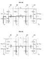
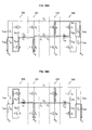
- FIGs. 6A to 6H are circuit diagrams showing the current path of each mode in the energy recovery circuit according to the first embodiment of the present invention.
- FIG. 7 is a diagram of a discharge current and a charge current of the capacitor in the energy recovery circuit according to the first embodiment of the present invention.
- FIG. 8 is an equivalent circuit diagram of mode 2 in the energy recovery circuit according to the first embodiment of the present invention.
- FIG. 9 is a diagram showing the wall charge status in a discharge cell.
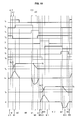
- FIG. 10 is a timing diagram of the energy recovery circuit according to a second embodiment of the present invention.
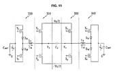
- FIG. 11 is a schematic circuit diagram of an energy recovery circuit according to a third embodiment of the present invention.
- FIG. 12 is a timing diagram of the energy recovery circuit according to the third embodiment of the present invention.
- FIGs. 13A to 13H are circuit diagrams showing the current path of each mode in the energy recovery circuit according to the third embodiment of the present invention.
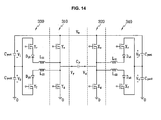
- FIG. 14 is a schematic circuit diagram of an energy recovery circuit according to a fourth embodiment of the present invention.
- FIG. 15 is a timing diagram of an energy recovery circuit according to a fifth embodiment of the present invention.
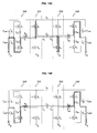
- FIGs. 16A to 16H are circuit diagrams showing the current path of each mode in the energy recovery circuit according to the fifth embodiment of the present invention.
- FIG. 3 is a schematic block diagram of a plasma display device according to the embodiment of the present invention.
- the plasma display device comprises, as shown in FIG. 3, a plasma display panel 100, an address driver 200, a scan/sustain driver 300, and a controller 400.
- the plasma display panel 100 comprises a plurality of address electrodes A 1 to A m arranged in columns, a plurality of scan electrodes Y 1 to Y n (hereinafter referred to as "Y electrodes”) and a plurality of sustain electrodes X 1 to X n (hereinafter referred to as "X electrodes”) alternately arranged in rows.
- the X electrodes X 1 to X n are formed in correspondence to the Y electrodes Y 1 to Y n , respectively.
- One terminal of each X electrode is connected to a terminal of each Y electrode.
- the controller 400 receives an external picture signal, generates an address drive control signal and a sustain control signal, and applies the generated control signals to the address driver 200 and the scan/sustain driver 300, respectively.
- the address driver 200 receives the address drive control signal from the controller 400, and applies a display data signal to each address electrode to select the discharge cells to be displayed.
- the scan/sustain driver 300 receives the sustain control signal from the controller 400, and applies sustain pulses alternately to the Y and X electrodes. The applied sustain pulses cause a sustain-discharge on the selected discharge cells.
- FIG. 4 is a schematic circuit diagram of an energy recovery circuit according to the first embodiment of the present invention.
- the energy recovery circuit comprises, as shown in FIG. 4, a Y electrode sustain unit 310, an X electrode sustain unit 320, a Y electrode charge/discharge unit 330, and an X electrode charge/discharge unit 340.
- the Y electrode sustain unit 310 is connected to the X electrode sustain unit 320, and a panel capacitor Cp is connected between the Y electrode sustain unit 310 and the X electrode sustain unit 320.
- the Y electrode sustain unit 310 includes switches Y s and Yg, and the X electrode sustain unit 320 includes switches X s and X g .
- the Y electrode charge/discharge unit 330 includes an inductor L 1 , switches Y r and Y f , and energy recovery capacitors C yer1 and C yer2
- the X electrode charge/discharge unit 340 includes an inductor L 2 , switches X r and X f , and energy recovery capacitors C xer1 and C xer2 .
- switches Y s , Y g , X s , X g , Y r , Y f , X r , and X f are preferably MOSFETs having a body diode, but may be any other switches that satisfy the following functions.
- Switches Y s and Y g are connected in series between a sustain discharge voltage V s and a ground voltage 0V, and switches X s and X g are connected in series between a sustain discharge voltage V s and a ground voltage 0V.
- the contact of switches Y s and Y g is connected to the Y electrode of panel capacitor C p
- the contact of switches X s and X g is connected to the X electrode of panel capacitor C p .
- the Y electrode charge/discharge unit 330 may further include diodes D y1 and D y2 for preventing a current path possibly formed by the body diodes of switches Y r and Y f .
- the Y electrode charge/discharge unit 330 charges the Y electrodes of the panel capacitor to the sustain discharge voltage V s or discharges such voltage to the ground voltage.
- one terminal of inductor L 2 is connected to the X electrode of panel capacitor C p , and switches X r and X f are connected in parallel between the other terminal of inductor L 2 and a contact of the energy recovery capacitors C xer1 and C xer2 .
- the X electrode charge/discharge unit 340 may further include diodes D x1 and D x2 for preventing a current path possibly formed by the body diodes of switches X r and X f .
- the X electrode charge/discharge unit 340 charges the X electrodes of the panel capacitor to the sustain discharge voltage V s or discharges such voltage to the ground voltage.
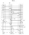
- FIG. 5 is a timing diagram of the energy recovery circuit according to the first embodiment of the present invention.
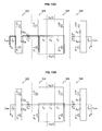
- FIGs. 6A to 6H are circuit diagrams showing the current path of each mode in the energy recovery circuit according to the first embodiment of the present invention.
- FIG. 7 is a diagram of a discharge current and a charge current of the capacitor in the energy recovery circuit according to the first embodiment of the present invention.
- FIG. 8 is an equivalent circuit diagram of mode 2 in the energy recovery circuit according to the first embodiment of the present invention.
- FIG. 9 is a diagram showing the wall charge status in a discharge cell.
- switches Y g and X g are in the "ON" state, so that the Y and X electrode voltages V y and V x of panel capacitor C p are both maintained at 0V.
- Capacitors C yer1 , C yer2 , C xer1 , and C xer2 are respectively charged with voltages V 1 , V 2 , V 3 , and V 4 .
- switch Y r is turned ON, with switches Y g and X g in the "ON" state. Then, a current I L1 flowing to inductor L 1 is increased with a slope of V s /2L 1 by a current path that includes capacitor C yer2 , switch Y r , inductor L 1 , and switch Y g in sequence. Energy is thus stored (charged) in inductor L 1 .
- switch Y g is turned OFF, with switches Y r and X g in the "ON" state. Then, a current path is formed that includes capacitor C yer2 , switch Y r , inductor L 1 , panel capacitor C p , and switch X g in sequence, thereby causing an LC resonance. Due to the resonance, the Y electrode voltage V y of panel capacitor C p is increased and panel capacitor C p is charged.
- switch Y s is turned ON when the Y electrode voltage V y has increased to V s .
- the Y electrode voltage V y cannot exceed V s due to the body diode of the switch Y s .
- the body diode of the switch Y s is automatically turned ON when the Y electrode V y equals V s .
- switch Y s (a channel of switch Y s ) is also turned ON. Accordingly, switch Y s is turned ON when the voltage between the drain and source is zero. In other words, with zero-voltage switching, there is no turn-on switching loss.
- switch Y r is turned OFF after current I L1 flowing to inductor L 1 becomes 0A.
- switches Y s and X g in the "ON" state, the Y and X electrode voltages V y and V x of panel capacitor C p are maintained at V s and 0V, respectively.
- switch Y f is turned ON with switches Y s and X g in the "ON" state. Then, a current path is formed through switch Y s , inductor L 1 , switch Y f , and capacitor C yer2 in sequence. Then, current I L1 flowing to inductor L 1 is decreased (i.e., the magnitude of current I L1 is increased), and energy is stored in inductor L 1 .
- switch Y s is turned OFF to form a current path through the body diode of switch X g , panel capacitor C p , inductor L 1 , switch Y f , and capacitor C yer2 in sequence, thereby causing an LC resonance. Due to the LC resonance, the Y electrode voltage V y of panel capacitor C p is decreased and the panel capacitor is discharged.
- switch Y g is turned ON when the Y electrode voltage V y is decreased to 0.
- the Y electrode voltage V y cannot exceed 0V due to the body diode of switch Y g .
- the body diode of switch Y g is automatically turned ON when the Y electrode voltage V y equals 0V.
- switch Y g (a channel of switch Y g ) is also turned ON. Accordingly, switch Y g is turned ON when the voltage between the drain and source is zero. In other words, with zero-voltage switching, there is no turn-on switching loss.
- switch Y g is turned ON, the Y electrode voltage V y is maintained at 0V.
- switch Y f is turned OFF after current I L1 flowing to inductor L 1 becomes 0A.
- switches Y g and X g in the "ON" state the Y and X electrode voltages V y and V x of panel capacitor C p are both maintained at 0V.
- the panel voltage (V y - V x ) swings between 0V and V s .
- switches X s , X g , X r , and X f and switches Y s , Yg, Y r , and Y f in modes 9 through 16 operate in the same manner as switches Y s , Yg, Y r , and Y f and switches X s , X g , X r , and X f operate in modes 1 through 8, respectively.
- the X electrode voltage V x of panel capacitor C p in modes 9 through 16 has the same waveform as the Y electrode voltage V y has in modes 1 through 8.
- the panel voltage V y - V x in modes 9 through 16 swings between 0V and -V s .
- the operation of the energy recovery circuit according to the first embodiment of the present invention in modes 9 through 16 will be understood by those skilled in the art and will not be described in detail.
- period ⁇ t 1 of mode 1 which is the period during which switches Y r and Y g are both turned ON
- period ⁇ t 5 of mode 5 which is the period during which switches Y s and Y f are both turned ON
- voltage V 2 of capacitor C yer2 becomes greater than voltage V 1 of capacitor C yer1 .
- the discharge current (i.e., energy) of capacitor C yer2 becomes less than the charge current (i.e., energy) of capacitor C yer2 .
- voltage V 2 of capacitor C yer2 remains at a level that is greater than voltage V 1 of capacitor C yer1 , which equals V s /2.
- the circuit state in mode 2 is modeled as shown in FIG. 8 by assuming that current I L1 flowing to inductor L 1 is I p1 at the time mode 1 ends, and capacitor C yer2 is a power source supplying V 2 .
- current I L1 flowing to inductor L 1 and the Y electrode voltage V y are given by Equations 1 and 2, respectively.
- Equations 1 and 2 ⁇ 1 and ⁇ are given by Equations 3 and 4, respectively.
- the magnitude of current I L1 reaches a maximum at time t pk , which occurs when sin( ⁇ t + ⁇ 1 ) is 1, or, equivalently, when, ( ⁇ t + ⁇ 1 ) is ⁇ /2.
- the Y electrode voltage V y is greater than V s /2.
- switch Y s performs zero-voltage switching.
- the Y electrode voltage V y is greater than V s /2 when the magnitude of current I L1 of inductor L 1 reaches its peak, the Y electrode voltage V y reaches the sustain-discharge voltage V s a short time after the magnitude of current I L1 is maximum. Accordingly, the rise time of the Y electrode voltage (the panel voltage) shortens.
- the panel voltage it is possible to increase the panel voltage to a sustain-discharge voltage V s because voltage V s of capacitor C yer2 is greater than V s /2. Also the energy stored in inductor can be used in discharge. In addition, the Y electrode voltage and the X electrode voltage are changed in an independent manner according to the first embodiment.
- capacitor C yer1 and C yer2 are used in the Y electrode charge/discharge unit 330.
- capacitor C yer1 can be removed. In this time, the current can be recovered to the sustain-discharge voltage V s in the mode 3.
- a power source other than capacitor C yer2 can be used for supplying voltage V 2 .
- the rise time and the fall time of the panel voltage can be different by controlling the periods of modes 1 and 5, which will now be described in detail.
- the Y electrode voltage V y becomes greater than V s /2 when the magnitude of current I L1 of inductor L 1 reaches its peak, because (V s -V 2 ) is less than V s . Accordingly, the Y electrode voltage V y becomes 0V a long time after the magnitude of current I L1 is at its maximum.
- the rise time of the Y electrode voltage is shorter than the fall time of the Y electrode voltage.
- the wall charge state of the regions between the X and Y electrodes of panel capacitor C p i.e., the discharge cells, is not uniform, so the wall voltage differs for each discharge cell, as illustrated in FIG. 9.
- the wall voltage V w1 is low and the discharge firing voltage is high.
- the wall voltage V w2 is high, and the discharge firing voltage is low. If the wall voltage is high as in discharge cell 112, discharge can occur during the rise of the panel voltage.
- Discharge begins during mode 2 in which switch Y s is in the "OFF" state, so that power for sustaining the discharge must be supplied from inductor L 1 as describe above. However, if the energy stored in inductor L 1 is not sufficient, the discharge that occurrs during the rise of the panel voltage is not sustained, and a second discharge occurs when switch Y s is turned ON. As discharge occurs twice, there is no uniform light emitted on the whole panel. Therefore, the rise time of the panel voltage is preferably short enough to prevent such a non-uniform discharge.
- a rapid decrease of the panel voltage may cause self-erasing of the wall charges by movement of resonant charges due to the rapid change of the electric field, resulting in a non-uniform distribution of the wall charges among discharge cells.
- a slow decrease of the panel voltage lowers the wall voltage due to recombination of spatial charges, causing no self-erasing.
- the fall time of the panel voltage is preferably longer than the rise time.
- voltage V 2 of capacitor C yer2 is greater than V s /2 so that the rise time of the panel voltage is shorter than the fall time of the panel voltage, thereby allowing a uniform light and a uniform wall charge state.
- the rise time and the fall time of the panel voltage can be controlled by controlling voltage V 2 .
- current I L1 flowing to inductor L 1 is the same when mode 1 ends and when mode 5 ends. Even if both currents differ, the rise time and the fall time of the panel voltage can be controlled by controlling the voltage V 2 .
- the panel voltage can be controlled by controlling the period of modes 1 and 5.
- FIG. 10 is a timing diagram of the energy recovery circuit according to a second embodiment of the present invention.
- time ⁇ t 1 of mode 1 is longer than time ⁇ t 5 of mode 5.
- current I p1 becomes greater than current I p5 because voltage V 2 is greater than voltage (V s -V 2 ).
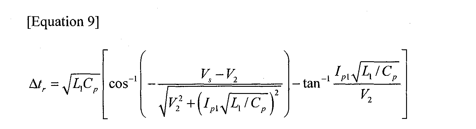
- the time ⁇ t r of mode 2 which is the rise time of the panel voltage, is given by Equation 9.
- the time ⁇ t f of mode 6 which is the fall time of the panel voltage, is given by Equation 10.
- the rise time of the panel voltage is shorter than the fall time of the panel voltage because current I p1 is greater than current I p5 and voltage V 2 is greater than voltage (V s -V 2 ).
- the Y electrode voltage V y is greater than V s /2 when the magnitude of current I L1 of inductor L 1 is at a maximum.
- the sustain-discharge voltage V s and the ground voltage 0V are applied to the Y and X electrodes in turn.
- V s /2 and -V s /2 can instead be applied to the Y and X electrodes in turn.
- a third embodiment of the present invention will now be described in detail, referring to FIGs. 11, 12, and 13A to 13H.
- FIG. 11 is a schematic circuit diagram of an energy recovery circuit according to a third embodiment of the present invention.
- FIG. 12 is a timing diagram of the energy recovery circuit according to the third embodiment of the present invention.
- FIGs. 13A to 13H are circuit diagrams showing the current path of each mode in the energy recovery circuit according to the third embodiment of the present invention.
- switches Y s and X s are connected to the voltage V s /2 corresponding to half of the sustain-discharge voltage V s
- switches Y g and X g are connected to the voltage - V s /2
- Switches Y r and Y f of the Y electrode charge/discharge unit 330 are connected to capacitor C yer2
- switches X r and X f of the X electrode charge/discharge unit 340 are connected to capacitor C xer2 .
- capacitors C yer1 and C xer1 of FIG. 4 are eliminated.
- capacitors C yer2 , and C xer2 are respectively charged with voltages V 2 and V 4 , which are both greater than 0V, corresponding to the mean value of the voltages V s /2 and -V s /2, and are both less than the voltage V s /2.
- the time of mode 1 is shorter than the time of mode 5 so that the discharge energy of capacitor C yer2 is less than the charge energy of capacitor C yer2 .
- switch Y r is turned ON, with switches Yg and X g in the "ON" state. Then, current I L1 flowing to inductor L 1 is increased with a slope of V s /2L 1 by a current path as shown in FIG. 13A. Energy is thus stored in inductor L 1 .
- switch Y g is turned OFF to form a current path as shown in FIG. 13B and cause an LC resonance. Due to the LC resonance, the Y electrode voltage V y of panel capacitor C p is increased, and panel capacitor C p is charged. As shown in FIG 12, the Y electrode voltage V y is greater than 0V at the time when the magnitude of current I L1 is maximum.
- switch Y s is turned ON when Y electrode voltage V y increases to V s /2.
- the Y electrode voltage V y cannot exceed V s /2 due to the body diode of switch Y s .
- switch Y s When switch Y s is turned ON, the Y electrode voltage V y is maintained at voltage V s /2. Accordingly, the panel voltage (V y - V x ) is maintained at the sustain-discharge voltage V s so that discharge occurs.
- current I L1 flowing to inductor L 1 is recovered to the voltage V s /2 on current path as illustrated in FIG. 13C.
- switch Y r is turned OFF after current I L1 flowing to inductor L 1 becomes 0A.
- switches Y s and X g in the "ON" state, the Y and X electrode voltages V y and V x of panel capacitor C p are maintained at V s /2 and -V s /2, respectively.
- switch Y f is turned ON with switches Y s and X g in the "ON" state. Then, a current path as shown in FIG. 13E is formed, and current I L1 flowing to inductor L 1 is decreased (i.e., the magnitude of current I L1 is increased). Energy is thus charged in inductor L 1 .
- switch Y s is turned OFF to form a current path shown in FIG. 13F, thereby causing an LC resonance. Due to the LC resonance, the Y electrode voltage V y is decreased and the panel capacitor is discharged. As shown in FIG 12, the Y electrode voltage V y is greater than 0V at the time when the magnitude of current I L1 is maximum.
- switch Y g is turned ON when the Y electrode voltage V y decreases to -V s /2.
- the Y electrode voltage V y cannot exceed -V s /2 due to the body diode of switch Y g .
- switch Y g When switch Y g is turned ON, the Y electrode voltage V y is maintained at the voltage -V s /2.
- current I L1 flowing to inductor L 1 is recovered to capacitor C yer2 on the current path as illustrated in FIG. 13G.
- switch Y f is turned OFF after current I L1 flowing to inductor L 1 becomes 0A.
- switches Y g and X g in the "ON" state the Y and X electrode voltages V y and V x of are both maintained at the voltage -V s /2.
- the panel voltage (V y - V x ) swings between 0V and V s .
- switches X s , X g , X r , and X f and switches Y s , Yg, Y r , and Y f in modes 9 through 16 operate in the same manner as switches Y s , Y g , Y r , and Y f and switches X s , X g , X r , and X f operate in modes 1 through 8, respectively.
- the driving voltage is lower than the driving voltage of the first embodiment because the maximum voltage applied to the Y and X electrodes is V S /2. Accordingly, switches having a low withstand voltage can be used in the Y and X electrode sustain unit.
- a power source for supplying the voltage between 0V and V s /2 can be used instead of capacitors C yer2 and C xer2 .
- the time period of mode 1 can be longer than the time period of mode 5 so that the rise time of the panel voltage is shorter than the fall time of the panel voltage, as described in the second embodiment of the present invention.
- the voltages V s /2 and -V s /2 are applied to the Y electrode.
- two voltages V h and (V h -V s ) having a voltage difference of V s can be applied to the Y electrode.
- inductor L 1 is used for increasing and decreasing the Y electrode voltage V y in the first through third embodiments of the present invention
- independent inductors can also be used for increasing and decreasing the Y electrode voltage V y . This embodiment will be described below in detail with reference to FIG. 14.
- FIG. 14 is a schematic circuit diagram of an energy recovery circuit according to a fourth embodiment of the present invention.
- inductors L 11 and L 12 are connected to the Y electrode of panel capacitor C p in place of inductor L 1
- two inductors L 21 and L 22 are connected to the X electrode of panel capacitor C p in place of inductor L 2
- Inductor L 11 is connected between the Y electrode and switch Y r
- inductor L 12 is connected between the Y electrode and switch Y f
- inductor L 21 is connected between the X electrode and switch X r
- inductor L 22 is connected between the X electrode and switch X f .
- power consumption is decreased because a current only flows in one direction in any one inductor.
- FIGs. 15, 16A to 16H is a timing diagram of an energy recovery circuit according to a fifth embodiment of the present invention.
- FIGs. 16A to 16H are circuit diagrams showing the current path of each mode in the energy recovery circuit according to the fifth embodiment of the present invention.
- the timing of the energy recovery circuit according to the fifth embodiment is different from that of the energy recovery circuit according to the first embodiment.
- modes 1 and 13, modes 2 and 14, modes 3 and 15, modes 5 and 9, modes 6 and 10, and modes 7 and 11 of FIG. 5 are overlapped, respectively. These correspond to modes 1, 2, 3, 5, 6, and 7 of FIG. 15, respectively.
- modes 8 and 16 of FIG. 5 are eliminated, and modes 4 and 12 of FIG. 5 correspond to modes 4 and 8 of FIG. 15.
- switch X f is initially turned ON, with switches Y g and X s in the "ON" state. Then a current path is formed through switch X s , inductor L 2 , switch X f , and capacitor C xer2 in sequence. After switch X f is turned ON, switch Y r is turned ON so that a current path is formed through capacitor C yer2 , switch Y r , inductor L 1 and switch Y g in sequence.
- switches Y g and X s are turned OFF, with switches Y r and X f in the "ON" state. Then, a current path is formed through capacitor C yer2 , switch Y r , inductor L 1 , panel capacitor Cp, inductor L 2 , switch X f , and capacitor C xer2 in sequence, thereby causing an LC resonance. Due to the resonance, the Y electrode voltage V y of panel capacitor C p increases and the X electrode voltage V x decreases.
- switches Y s and X g are turned ON when the Y electrode voltage V y has increased to V s and the X electrode voltage V x has decreased to 0V.
- the Y electrode voltage V y cannot exceed V s due to the body diode of switch Y s .
- the body diode of switch Y s is automatically turned ON when the Y electrode V y equals V s .
- the X electrode voltage V x cannot exceed 0V due to the body diode of switch X g .
- the body diode of switch X g is automatically turned ON when the Y electrode V x equals 0V.
- current I L1 flowing to inductor L 1 is recovered to the path through switch Y r , inductor L 1 , the body diode of switch Y s , and capacitor C yer1 in sequence.
- the current I L2 flowing to inductor L 2 is recovered to the path through the body diode of switch X g , inductor L 2 , switch X f , and capacitor C xer2 in sequence.
- switch X f is turned OFF when current I L2 flowing to inductor L 2 becomes 0A.
- switch Y r is turned OFF when current I L1 flowing to inductor L 1 becomes 0A.
- switch Y f is turned ON with switches Y s and X g in the "ON" state. Then, a current path is formed through switch Y s , inductor L 1 , switch Y f , and capacitor C yer2 in sequence. After switch Y f is turned ON, switch X r is turned ON so that a current path is formed through capacitor C xer2 , switch X r , inductor L 2 , and switch X g in sequence. Thus, energy is stored (charged) in inductors L 1 and L 2 .
- switches Y s and X g are turned OFF, with switches Y f and X r in the "ON" state. Then a current path is formed through capacitor C xer2 , switch X r , inductor L 2 , panel capacitor C p , inductor L 1 , switch Y f , and capacitor C yer2 in sequence, thereby causing an LC resonance. Due to the resonance, the Y electrode voltage V y of panel capacitor C p decreases and the X electrode voltage V x increases.
- switches Y g and X s are turned ON when the Y electrode voltage V y has decreased to 0V and the X electrode voltage V x has increased to V s .
- the Y electrode voltage V y cannot exceed 0V due to the body diode of switch Y g
- the X electrode voltage V x cannot exceed V s due to the body diode of switch X s .
- switch Y f is turned OFF when current I L1 flowing to inductor L 1 becomes 0A.
- switch X r is turned OFF when current I L2 flowing to inductor L 2 becomes 0A.
- the time period during which switches Y r and Y g are both turned ON in mode 1 is shorter than the time period during which switches Y s and Y f are both turned ON in mode 5.
- the discharge energy of capacitor C yer2 is less than the charge energy of capacitor C yer2
- voltage V 2 of capacitor C yer2 remains at a level that is greater than V s /2.
- the time period during which switches X f and X s are both turned ON in mode 1 is longer than the time period during which switches X r and X g are both turned ON in mode 5, so that the charge energy of capacitor C xer2 is greater than the discharge energy of capacitor C xer2 , and voltage V 2 of capacitor C xer2 remains at a level greater than V s /2.
- the panel voltage (V y - V x ) swings between -V s and V s .
- switches X s , X g , X r , and X f and switches Y s , Y g , Y r , and Y f in modes 9 through 16 operate in the same manner as switches Y s , Y g , Y r , and Y f and switches X s , X g , X r , and X f operate in modes 1 through 8, respectively.
- the driving method according to the second through fourth embodiments of the present invention can also be adapted to the driving method of the fifth embodiment of the present invention.
- the energy recovery circuit is described in the embodiments of the present invention as connected to the Y electrode of the panel. However, as mentioned above, this energy recovery circuit can also be applied to the X electrode. Also, when the applied voltage is changed, this circuit can be applied to the address electrode.
Landscapes
- Engineering & Computer Science (AREA)
- Physics & Mathematics (AREA)
- Power Engineering (AREA)
- Plasma & Fusion (AREA)
- Computer Hardware Design (AREA)
- General Physics & Mathematics (AREA)
- Theoretical Computer Science (AREA)
- Control Of Indicators Other Than Cathode Ray Tubes (AREA)
- Control Of Gas Discharge Display Tubes (AREA)
- Transforming Electric Information Into Light Information (AREA)
Abstract
Description
where the third voltage is between a fourth voltage, which corresponds to the mean value of the first and second voltages, and the second voltage.
the third voltage is between a fourth voltage, which corresponds to the mean value of the first and second voltages, and the second voltage.

Claims (51)
- A device for driving a plasma display panel, which has first and second electrodes with a panel capacitor formed therebetween, the device comprising:wherein the charge/discharge unit changes the voltage of the first electrode from the first voltage to a third voltage while increasing the magnitude of a current flowing in the first inductor, and changes the voltage of the first electrode from the third voltage to the second voltage while decreasing the magnitude of the current flowing in the first inductor; anda charge/discharge unit comprising a first inductor coupled to the first electrode, the charge/discharge unit changing the voltage of the first electrode from a first voltage to a second voltage by using the first inductor; anda sustain unit maintaining the voltage of the first electrode at the second voltage during a predetermined period after the voltage of the first electrode is changed to the second voltage,
the third voltage is between a fourth voltage corresponding to the mean value of the first and second voltages and the second voltage. - The device as claimed in claim 1, wherein the charge/discharge unit changes the voltage of the first electrode by using the first inductor after storing a first energy in the first inductor.
- The device as claimed in claim 2, wherein the sustain unit maintains the voltage of the second electrode at the first voltage while the voltage of the first electrode is changed to and maintained at the second voltage.
- The device as claimed in claim 3, wherein the charge/discharge unit changes the voltage of the first electrode on a path including a fifth voltage being between the fourth and second voltages, the first inductor, and the panel capacitor in sequence.
- The device as claimed in claim 4, wherein the charge/discharge further comprises a capacitor charged to the fifth voltage.
- The device as claimed in claim 5, wherein a second energy is maintained in the first inductor after the voltage of the first electrode is changed to the second voltage.
- The device as claimed in claim 6, wherein the first energy is greater than the second energy.
- The device as claimed in claim 6, wherein the first energy is less than the second energy.
- The device as claimed in claim 6, wherein the first energy is equal to the second energy.
- The device as claimed in claim 4, wherein the charge/discharge unit changes the voltage of the first electrode from the second voltage to the first voltage, while the sustain unit maintains the voltage of the second electrode at the first voltage.
- The device as claimed in claim 10, wherein the charge/discharge unit changes the voltage of the first electrode from the second voltage to a sixth voltage while increasing the magnitude of the current flowing in the first inductor, and changes the voltage of the first electrode from the sixth voltage to the first voltage while decreasing the magnitude of the current flowing in the first inductor; and
the sixth voltage is between the fourth and second voltages. - The device as claimed in claim 11, wherein the charge/discharge unit changes the voltage of the first electrode to the first voltage on a path including the panel capacitor, the first inductor, and the fifth voltage in sequence.
- The device as claimed in claim 4, wherein the difference between the first and second voltages is a sustain-discharge voltage.
- The device as claimed in claim 13, wherein either the first voltage or the second voltage is a ground voltage.
- The device as claimed in claim 13, wherein either the first voltage or the second voltage is a voltage corresponding to half of a sustain-discharge voltage.
- The device as claimed in claim 1, wherein the charge/discharge unit comprises a second inductor coupled to the second electrode and changes the voltage of the second electrode from the second voltage to the first voltage by using the second inductor while changing the voltage of the first electrode from the first voltage to the second voltage; and
the sustain unit maintains the voltage of the second electrode at the first voltage during the predetermined period after the voltage of the second electrode is changed to the first voltage. - The device as claimed in claim 16, wherein the charge/discharge unit changes the voltage of the second electrode from the second voltage to a fifth voltage while increasing the magnitude of a current flowing in the second inductor and changes the voltage of the second electrode from the fifth voltage to the first voltage while decreasing the magnitude of the current flowing in the second inductor; and
the fifth voltage is between the fourth and first voltages. - The device as claimed in claim 16, wherein the charge/discharge unit changes the voltage of the second electrode by using the second inductor after storing a second energy in the second inductor.
- A method for driving a plasma display panel, which has first and second electrodes with a panel capacitor formed therebetween, the method comprising:wherein the first voltage is between a third voltage corresponding to half of the second voltage and the second voltage.charging the panel capacitor to a first voltage, while increasing the magnitude of a current flowing in a first inductor coupled to the first electrode; andcharging the panel capacitor from the first voltage to a second voltage while decreasing the magnitude of the current flowing in the first inductor,
- The method as claimed in claim 19, wherein the second voltage is a sustain-discharge voltage.
- The method as claimed in claim 19, further comprising: storing a first energy in the first inductor before charging the panel capacitor to a first voltage.
- The method as claimed in claim 21, wherein a voltage of the second electrode is maintained at a fourth voltage while charging the panel capacitor to the second voltage.
- The method as claimed in claim 22, wherein the panel capacitor is charged on a path including a fifth voltage, the first inductor, and the panel capacitor in sequence; and
the difference between the fifth voltage and the fourth voltage is between the third voltage and the second voltage. - The method as claimed in claim 23, wherein the fifth voltage is supplied from a capacitor.
- The method as claimed in claim 21, wherein a second energy, which is maintained in the first inductor after charging the panel capacitor to the second voltage, is less than the first energy.
- The method as claimed in claim 21, wherein a second energy, which is maintained in the first inductor after charging the panel capacitor to the second voltage, is greater than the first energy.
- The method as claimed in claim 21, wherein a second energy, which is maintained in the first inductor after charging the panel capacitor to the second voltage, is equal to the first energy.
- The method as claimed in claim 19, further comprising:discharging the panel capacitor to a fourth voltage, while increasing the magnitude of the current flowing in the first inductor; anddischarging the panel capacitor from the fourth voltage to a ground voltage, while decreasing the magnitude of the current flowing in the first inductor.
- The method as claimed in claim 28, wherein the fourth voltage is between the third voltage and the second voltage.
- The method as claimed in claim 28, wherein a time period for charging the panel capacitor to the second voltage is shorter than a time period for discharging the panel capacitor to the ground voltage.
- The method as claimed in claim 28, further comprising:storing a first energy in the first inductor before charging the panel capacitor to the first voltage; andstoring a second energy in the first inductor before discharging the panel capacitor to the fourth voltage.
- The method as claimed in claim 31, wherein the first energy is greater than the second energy.
- The method as claimed in claim 21, wherein both a voltage of the first electrode and a voltage of the second electrode are changed while charging the panel capacitor to the second voltage.
- The method as claimed in claim 33, wherein one voltage of the first and second electrodes is increased and the other voltage is decreased to charge the panel capacitor to the second voltage.
- The method as claimed in claim 34, wherein the voltage of the second electrode is changed by a second inductor coupled to the second electrode.
- The method as claimed in claim 35, further comprising:storing a second energy in the second inductor before charging the panel capacitor to the first voltage.
- A method for driving a plasma display panel, which has first and second electrodes with a panel capacitor formed therebetween, the method comprising:wherein the voltage of the first electrode is firstly changed from the first voltage to a third voltage while increasing the magnitude of a current flowing in the first inductor and secondly changed from the third voltage to the second voltage while decreasing the magnitude of the current flowing in the first inductor; andinjecting a current of a first direction to a first inductor coupled to the first electrode to store a first energy, while a voltage of the first electrode and a voltage of the second electrode are both maintained at a first voltage;changing the voltage of the first electrode to a second voltage by using a resonance between the first inductor and the panel capacitor and the first energy, while the voltage of the second electrode is maintained at the first voltage; andmaintaining the voltage of the first electrode and the voltage of the second electrode at the second voltage and the first voltage, respectively,
the third voltage is between a fourth voltage corresponding to the mean value of the first and second voltages and the second voltage. - The method as claimed in claim 37, wherein the difference between the first voltage and the second voltage is a sustain-discharge voltage.
- The method as claimed in claim 37, wherein an energy remaining in the first inductor is decreased while maintaining the voltage of the first electrode and the voltage of the second electrode at the second voltage and the first voltage, respectively.
- The method as claimed in claim 37, further comprising:injecting a current of a second direction to a second inductor coupled to the first electrode to store a second energy while the voltage of the first electrode and the voltage of the second electrode are both maintained at the second voltage; andchanging the voltage of the first electrode to the first voltage by using a resonance between the second inductor and the panel capacitor and the second energy while the voltage of the second electrode is maintained at the second voltage.
- The method as claimed in claim 40, wherein the second inductor is the first inductor, and the second direction is opposite to the first direction.
- A method for driving a plasma display panel, which has first and second electrodes with a panel capacitor formed therebetween, the method comprising:wherein the voltage of the first electrode is firstly changed from the first voltage to a third voltage while increasing the magnitude of a current flowing in the first inductor and secondly changed from the third voltage to the second voltage while decreasing the magnitude of the current flowing in the first inductor; andinjecting a current of a first direction to a first inductor coupled to the first electrode to store a first energy, and injecting a current of a second direction to a second inductor coupled to the second electrode to store a second energy;changing the voltage of the first electrode from a first voltage to a second voltage and the voltage of the second electrode from the second voltage to the first voltage by using a resonance between the first and second inductors and the panel capacitor and the first and second energies; andmaintaining the voltage of the first electrode and the voltage of the second electrode at the second voltage and the first voltage, respectively,
the third voltage is between a fourth voltage corresponding to the mean value of the first and second voltages and the second voltage. - The method as claimed in claim 42, wherein the difference between the first voltage and the second voltage is a sustain-discharge voltage.
- The method as claimed in claim 37, wherein energies remaining in the first and second inductors are decreased while maintaining the voltage of the first electrode and the voltage of the second electrode at the second voltage and the first voltage, respectively.
- The method as claimed in claim 37, further comprising:injecting a current of a third direction to a third inductor coupled to the first electrode to store a third energy, and injecting a current of a fourth direction to a fourth inductor coupled to the second electrode to store a fourth energy; andchanging the voltage of the first electrode from the second voltage to the first voltage and the voltage of the second electrode from the first voltage to the second voltage by using a resonance between the third and fourth inductors and the panel capacitor and the third and fourth energies.
- The method as claimed in claim 45, wherein the third inductor is the first inductor, and the third direction is opposite to the first direction; and
the fourth inductor is the second inductor, and the fourth direction is opposite to the second direction. - A plasma display device, comprising:wherein the driving circuit firstly charges the panel capacitor to a voltage greater than half of a desired voltage while increasing the magnitude of a current flowing in the inductor, and secondly charges the panel capacitor to the desired voltage while decreasing the magnitude of the current flowing in the inductor.a plasma display panel having first and second electrodes with a panel capacitor formed therebetween; anda driving circuit comprising an inductor coupled to the first electrode, the driving circuit applying a driving voltage to the first electrode,
- The plasma display device as claimed in claim 47, wherein the driving circuit stores energy in the inductor before charging the panel capacitor.
- A plasma display device, comprising:wherein the driving circuit firstly charges the panel capacitor to a voltage greater than half of a desired voltage while increasing the magnitude of a current flowing in the first inductor, and secondly charges the panel capacitor to the desired voltage while decreasing the magnitude of the current flowing in the first inductor; anda plasma display panel having first and second electrodes with a panel capacitor formed therebetween; anda driving circuit comprising first and second inductors coupled to the first electrode in parallel, the driving circuit applying a driving voltage to the first electrode,
the driving circuit discharges the panel capacitor by using the second inductor. - The plasma display device as claimed in claim 49, wherein the driving circuit stores a first energy in the first inductor before charging the panel capacitor.
- The plasma display device as claimed in claim 51, wherein the driving circuit stores a second energy in the second inductor before discharging the panel capacitor.
Applications Claiming Priority (2)
| Application Number | Priority Date | Filing Date | Title |
|---|---|---|---|
| KR2003052519 | 2003-07-30 | ||
| KR10-2003-0052519A KR100502931B1 (en) | 2003-07-30 | 2003-07-30 | Driving device and method of plasma display panel and plasma display device |
Publications (2)
| Publication Number | Publication Date |
|---|---|
| EP1503362A2 true EP1503362A2 (en) | 2005-02-02 |
| EP1503362A3 EP1503362A3 (en) | 2007-09-05 |
Family
ID=33536460
Family Applications (1)
| Application Number | Title | Priority Date | Filing Date |
|---|---|---|---|
| EP04090298A Withdrawn EP1503362A3 (en) | 2003-07-30 | 2004-07-27 | Device and method for driving a plasma display panel, and a plasma display device |
Country Status (5)
| Country | Link |
|---|---|
| US (1) | US20050200562A1 (en) |
| EP (1) | EP1503362A3 (en) |
| JP (1) | JP2005049814A (en) |
| KR (1) | KR100502931B1 (en) |
| CN (2) | CN101546514A (en) |
Cited By (3)
| Publication number | Priority date | Publication date | Assignee | Title |
|---|---|---|---|---|
| EP1739646A3 (en) * | 2005-06-28 | 2007-08-01 | LG Electronics Inc. | Plasma display apparatus and method of driving the same |
| EP1860635A3 (en) * | 2006-05-26 | 2009-08-26 | LG Electronic Inc. | Driving method for plasma display apparatus |
| EP1679684A3 (en) * | 2005-01-10 | 2010-04-14 | LG Electronics Inc. | Sustain pulse controller for a plasma display apparatus |
Families Citing this family (10)
| Publication number | Priority date | Publication date | Assignee | Title |
|---|---|---|---|---|
| EP1632928A3 (en) * | 2004-09-07 | 2006-10-11 | LG Electronic Inc. | Energy recovery apparatus and method for a plasma display panel |
| KR100692822B1 (en) * | 2005-06-28 | 2007-03-09 | 엘지전자 주식회사 | Energy recovery device and recovery method of plasma display panel |
| TWI299153B (en) * | 2005-10-24 | 2008-07-21 | Chunghwa Picture Tubes Ltd | Circuit and method for resetting plasma display panel |
| KR100747162B1 (en) * | 2005-12-06 | 2007-08-07 | 엘지전자 주식회사 | Plasma display device |
| KR100820668B1 (en) * | 2006-09-12 | 2008-04-11 | 엘지전자 주식회사 | Plasma display device |
| JP2008175953A (en) * | 2007-01-17 | 2008-07-31 | Hitachi Plasma Display Ltd | Plasma display device |
| JPWO2009130860A1 (en) * | 2008-04-22 | 2011-08-11 | パナソニック株式会社 | Plasma display apparatus and driving method of plasma display panel |
| CN101727822B (en) * | 2008-12-29 | 2011-12-07 | 四川虹欧显示器件有限公司 | Scanning electrode driving circuit and driving method for plasma display |
| WO2012001696A1 (en) * | 2010-06-28 | 2012-01-05 | Kamalabai Russeel Rajeev | Electrons enhancement circuit |
| CN109493808B (en) * | 2017-09-12 | 2020-11-17 | 元太科技工业股份有限公司 | display device |
Family Cites Families (10)
| Publication number | Priority date | Publication date | Assignee | Title |
|---|---|---|---|---|
| US4866349A (en) * | 1986-09-25 | 1989-09-12 | The Board Of Trustees Of The University Of Illinois | Power efficient sustain drivers and address drivers for plasma panel |
| JP3897896B2 (en) * | 1997-07-16 | 2007-03-28 | 三菱電機株式会社 | Plasma display panel driving method and plasma display device |
| JP3242096B1 (en) * | 1999-11-12 | 2001-12-25 | 松下電器産業株式会社 | Display device and display method thereof |
| TW526459B (en) * | 2000-06-23 | 2003-04-01 | Au Optronics Corp | Plasma display holding-stage driving circuit with discharging current compensation function |
| CN1208749C (en) * | 2000-10-09 | 2005-06-29 | 友达光电股份有限公司 | Power saving drive circuit |
| US7138994B2 (en) * | 2000-11-09 | 2006-11-21 | Lg Electronics Inc. | Energy recovering circuit with boosting voltage-up and energy efficient method using the same |
| JP2003015595A (en) * | 2001-06-29 | 2003-01-17 | Pioneer Electronic Corp | Drive circuit for PDP display device |
| US6963174B2 (en) * | 2001-08-06 | 2005-11-08 | Samsung Sdi Co., Ltd. | Apparatus and method for driving a plasma display panel |
| KR100477985B1 (en) * | 2001-10-29 | 2005-03-23 | 삼성에스디아이 주식회사 | A plasma display panel, a driving apparatus and a method of the plasma display panel |
| US6850213B2 (en) * | 2001-11-09 | 2005-02-01 | Matsushita Electric Industrial Co., Ltd. | Energy recovery circuit for driving a capacitive load |
-
2003
- 2003-07-30 KR KR10-2003-0052519A patent/KR100502931B1/en not_active Expired - Fee Related
-
2004
- 2004-02-20 JP JP2004044365A patent/JP2005049814A/en active Pending
- 2004-07-22 US US10/895,970 patent/US20050200562A1/en not_active Abandoned
- 2004-07-27 EP EP04090298A patent/EP1503362A3/en not_active Withdrawn
- 2004-07-30 CN CN200910128036A patent/CN101546514A/en active Pending
- 2004-07-30 CN CNB2004100556076A patent/CN100543816C/en not_active Expired - Fee Related
Cited By (3)
| Publication number | Priority date | Publication date | Assignee | Title |
|---|---|---|---|---|
| EP1679684A3 (en) * | 2005-01-10 | 2010-04-14 | LG Electronics Inc. | Sustain pulse controller for a plasma display apparatus |
| EP1739646A3 (en) * | 2005-06-28 | 2007-08-01 | LG Electronics Inc. | Plasma display apparatus and method of driving the same |
| EP1860635A3 (en) * | 2006-05-26 | 2009-08-26 | LG Electronic Inc. | Driving method for plasma display apparatus |
Also Published As
| Publication number | Publication date |
|---|---|
| US20050200562A1 (en) | 2005-09-15 |
| KR100502931B1 (en) | 2005-07-21 |
| CN1577439A (en) | 2005-02-09 |
| CN101546514A (en) | 2009-09-30 |
| KR20050014076A (en) | 2005-02-07 |
| EP1503362A3 (en) | 2007-09-05 |
| CN100543816C (en) | 2009-09-23 |
| JP2005049814A (en) | 2005-02-24 |
Similar Documents
| Publication | Publication Date | Title |
|---|---|---|
| US7027010B2 (en) | Plasma display panel, and apparatus and method for driving the same | |
| US7839358B2 (en) | Apparatus and method for driving a plasma display panel | |
| KR100463185B1 (en) | A plasma display panel, a driving apparatus and a method of the plasma display panel | |
| US7023139B2 (en) | Apparatus and method for driving plasma display panel | |
| KR100467448B1 (en) | Plasma display panel and driving apparatus and method thereof | |
| US7379033B2 (en) | Plasma display device and driving method of plasma display panel | |
| US20050200562A1 (en) | Device and method for driving a plasma display panel, and a plasma display device | |
| US7170474B2 (en) | Plasma display panel driver, driving method thereof, and plasma display device | |
| US7307601B2 (en) | Driving method and device of plasma display panel and plasma display device | |
| US6727659B2 (en) | Apparatus and method for driving plasma display panels | |
| KR100560516B1 (en) | Driving Method of Plasma Display and Plasma Display Panel | |
| KR100502906B1 (en) | Driving method of plasma display panel | |
| KR100490636B1 (en) | A plasma display panel, a driving apparatus and a method of the plasma display panel | |
| KR100502934B1 (en) | A plasma display panel, a driving apparatus and a method of the plasma display panel | |
| KR100521482B1 (en) | A driving method of plasma display panel | |
| KR100502913B1 (en) | Driving apparatus and method of plasma display panel | |
| KR20050120201A (en) | A driving method of plasma display panel and plasma display device |
Legal Events
| Date | Code | Title | Description |
|---|---|---|---|
| PUAI | Public reference made under article 153(3) epc to a published international application that has entered the european phase |
Free format text: ORIGINAL CODE: 0009012 |
|
| AK | Designated contracting states |
Kind code of ref document: A2 Designated state(s): AT BE BG CH CY CZ DE DK EE ES FI FR GB GR HU IE IT LI LU MC NL PL PT RO SE SI SK TR |
|
| AX | Request for extension of the european patent |
Extension state: AL HR LT LV MK |
|
| PUAL | Search report despatched |
Free format text: ORIGINAL CODE: 0009013 |
|
| AK | Designated contracting states |
Kind code of ref document: A3 Designated state(s): AT BE BG CH CY CZ DE DK EE ES FI FR GB GR HU IE IT LI LU MC NL PL PT RO SE SI SK TR |
|
| AX | Request for extension of the european patent |
Extension state: AL HR LT LV MK |
|
| 17P | Request for examination filed |
Effective date: 20071105 |
|
| AKX | Designation fees paid |
Designated state(s): DE FR GB NL |
|
| 17Q | First examination report despatched |
Effective date: 20090617 |
|
| STAA | Information on the status of an ep patent application or granted ep patent |
Free format text: STATUS: THE APPLICATION IS DEEMED TO BE WITHDRAWN |
|
| 18D | Application deemed to be withdrawn |
Effective date: 20110201 |