EP1502353B1 - Rauscharmer verstärker mit variabler verstärkung und hoher dynamik - Google Patents
Rauscharmer verstärker mit variabler verstärkung und hoher dynamik Download PDFInfo
- Publication number
- EP1502353B1 EP1502353B1 EP03740687.3A EP03740687A EP1502353B1 EP 1502353 B1 EP1502353 B1 EP 1502353B1 EP 03740687 A EP03740687 A EP 03740687A EP 1502353 B1 EP1502353 B1 EP 1502353B1
- Authority
- EP
- European Patent Office
- Prior art keywords
- gain
- amplifier
- variable
- circuit
- varicaps
- Prior art date
- Legal status (The legal status is an assumption and is not a legal conclusion. Google has not performed a legal analysis and makes no representation as to the accuracy of the status listed.)
- Expired - Lifetime
Links
- 239000003990 capacitor Substances 0.000 description 15
- 238000010586 diagram Methods 0.000 description 9
- 238000002604 ultrasonography Methods 0.000 description 7
- 239000000523 sample Substances 0.000 description 5
- 238000004519 manufacturing process Methods 0.000 description 4
- 238000002592 echocardiography Methods 0.000 description 3
- 230000001419 dependent effect Effects 0.000 description 2
- 230000001174 ascending effect Effects 0.000 description 1
- 230000007423 decrease Effects 0.000 description 1
- 239000006185 dispersion Substances 0.000 description 1
- 238000000034 method Methods 0.000 description 1
Images


Classifications
-
- H—ELECTRICITY
- H03—ELECTRONIC CIRCUITRY
- H03G—CONTROL OF AMPLIFICATION
- H03G3/00—Gain control in amplifiers or frequency changers
- H03G3/20—Automatic control
- H03G3/30—Automatic control in amplifiers having semiconductor devices
-
- H—ELECTRICITY
- H03—ELECTRONIC CIRCUITRY
- H03G—CONTROL OF AMPLIFICATION
- H03G1/00—Details of arrangements for controlling amplification
- H03G1/0005—Circuits characterised by the type of controlling devices operated by a controlling current or voltage signal
- H03G1/0035—Circuits characterised by the type of controlling devices operated by a controlling current or voltage signal using continuously variable impedance elements
- H03G1/0052—Circuits characterised by the type of controlling devices operated by a controlling current or voltage signal using continuously variable impedance elements using diodes
- H03G1/0064—Variable capacitance diodes
-
- H—ELECTRICITY
- H03—ELECTRONIC CIRCUITRY
- H03F—AMPLIFIERS
- H03F1/00—Details of amplifiers with only discharge tubes, only semiconductor devices or only unspecified devices as amplifying elements
- H03F1/26—Modifications of amplifiers to reduce influence of noise generated by amplifying elements
-
- H—ELECTRICITY
- H03—ELECTRONIC CIRCUITRY
- H03G—CONTROL OF AMPLIFICATION
- H03G1/00—Details of arrangements for controlling amplification
Definitions
- the present invention as defined in independent claim 1 relates to a high dynamic gain variable gain and low noise amplifier arrangement.
- Variable gain amplifiers and low noise are used, among others, in ultrasound.
- the echoes collected by the ultrasound probes of these ultrasound machines are all low level, and the ratio between the level of the weakest echoes and that of the weakest echoes can be very important (more than 100 dB).
- the capacity variation range of common varicaps is not very wide. Only special varicaps, very expensive, would be suitable, and they are all the more expensive that the usual technology of manufacturing these diodes is BICmos type, which requires to select in a series of manufacture those with the largest range of variation of capacity.
- variable gain amplifier circuit comprising between the output of its amplifier and its inverting input a first impedance, and between the same inverting input and the signal source to be amplified a second impedance, these impedances being capacitive reactive impedances, at least one of them being variable.
- the second impedance is in series with the impedance of the signal source, so that the gain of the assembly is dependent on the impedance of the source.
- this source is an ultrasound probe (operating at frequencies of several MHz), its impedance is not capacitive, and the gain of the assembly varies greatly depending on the frequency if one wants that this assembly is to very low noise.
- the value of the second impedance would have to be much higher than that of the probe. In this case, the noise produced by the amplifier (this noise is substantially proportional to the input impedance) would be much too important.
- the gain of the amplifier would be limited, because, to have a high gain, it would be necessary that the value of the first impedance is much higher than that of the second (which should itself be much higher that of the source), which would require to have too high values for the first two impedances, and their behavior at high frequencies would be very difficult to control.
- the present invention relates to a low-noise variable gain amplifier circuit whose gain variation has the greatest possible dynamic range, this gain being the least dependent on the frequency of the signals to be amplified and the output impedance of the amplifier.
- the source of these signals and which allows the use of currently available reactive components low range of reactance, these components can be made according to a conventional technology such as BICmos.
- the amplifier assembly according to the invention of the operational amplifier type whose output is connected by a first reactive element to one of its inputs, this input being further connected by a second reactive element to a common pole of the power supply.
- the amplifier is characterized in that the input of the amplifier to which the two reactive elements are connected is its inverting input, and that its non-inverting input is connected to the signal source to be amplified.
- the reactive elements are elements with variable capacity, preferably Varicaps.
- each variable capacity element comprises at least two varicaps.
- the present invention is described herein with reference to an echo signal amplifier for an ultrasound apparatus, but it is understood that it is not limited to this single application, and that it can be implemented in many other applications requiring a variable gain amplifier with wide range of gain over a wide frequency range, to amplify signals that can be very low level.
- FIG. 1 a circuit 1 with an operational amplifier 2 in conventional assembly, whose non-inverting input receives from a pole of a source 3, signals to be amplified, the other pole of this source being connected to ground, and whose inverting input is connected to its output by a reactance 4, impedance Z1.
- the inverting input of the amplifier 2 is also connected to ground by a reactor 5, impedance Z2.
- the value of the impedance Z1 and / or of the impedance Z2 must be varied.
- the reactance 4 is of the impedance type varying as a function of a control voltage.
- the law of variation of this impedance is not necessarily linear as a function of the variations of the control voltage.
- the circuit producing the variable control voltage can memorize the law linking the variations of the control voltage to the impedance variations.
- Element 4 may be a resistor, but in general it is a capacitive element.
- the two reactances 4 and 5 are capacitive elements whose value of the capacitance is variable and controlled in tension.
- they are diodes with variable capacity, called "Varicaps".
- Varicap diode is a diode whose intrinsic capacity varies greatly depending on the reverse voltage applied to it. This voltage will be referred to hereafter as control voltage V C.
- the Varicap diodes used as elements 4 and 5 are apairées, such a characteristic being important for the realization of a specific integrated circuit 1. Indeed, it is well known that the values of the characteristic parameters of components have a significant dispersion in the same series of manufacture, but the tolerance on the ratio of the characteristics of two similar components is always narrow. Thanks to this characteristic, the gain of the circuit 1 with varicaps as elements 4 and 5 becomes practically independent of the series of manufacture in which the varicaps are taken, because this gain depends on the ratio of two similar components, taken in the same series.
- variable impedance reactors widens the variation range of the gain of the variable gain amplifier 1. In fact, when the value of Z1 increases, that of Z2 decreases, and vice versa.
- the range of the theoretical range of gain variation is substantially equal to the square of the extent of that of the circuit of the prior art to a single varicap.
- the assembly of the invention has a very high input impedance, so that its gain is practically independent of the impedance of the source 3.
- the capacitance value of the impedance Z2 can be easily chosen very low (some tens of pF, for example), so that even at frequencies of about ten MHz, or more, its impedance remains very low.
- the value of the impedance Z1 can then be low enough so that it can be a varicap. As a result, the noise of the amplifier 2 remains very low.
- FIG 2 the simplified diagram of a variable gain amplifier 6 according to the invention.
- This amplifier 6 comprises the elements 7 to 10, respectively similar to the elements 2 to 5 of the figure 1 , and a circuit 11 for controlling the reverse voltage applied to the varicaps 9 and 10, that is to say providing said control voltage V C.
- the figure 3 shows the detailed diagram of an exemplary embodiment 12 of the "amplifier" part (that is to say without the control circuit 11) of the variable gain amplifier 6 of the figure 2 .
- This amplifier arrangement 12 comprises an operational amplifier 13, powered symmetrically by being connected on one side to a supply voltage terminal + V DC , and on the other to a supply voltage terminal -V DC .
- a source 18 of signals to be amplified (for example an ultrasonic probe) is connected to the non-inverting input of amplifier 13 by a series resistor 19 and a transformer 20.
- the inverting input of the amplifier 13 is connected, on the one hand, to its output by a circuit 21, and on the other hand, to ground (which represents the common pole of the supply voltages + V DC and - V CC ) by a circuit 22.
- These circuits 21 and 22 respectively correspond to the reactances 9 and 10 of the figure 2 .
- the circuit 21 comprises a resistor 23 connected between the output and the inverting input of the amplifier 13. In parallel with the resistor 23, is connected a series circuit consisting of a resistor 24, a capacitor 25, a diode varicap 26 and a capacitor 27. The cathode of the diode 26 is connected by a resistor 28, in series with a resistor 29, to a terminal 30 on which is applied a first gain control voltage TC1. The common point of the resistors 28 and 29 is connected to ground by a capacitor 31.
- a capacitor 32 is connected on the one hand and a series circuit on the other hand comprising a varicap diode 33 and a capacitor 34, the cathode of the diode 33 being connected to the anode of the diode 26.
- the point common to the anode of the diode 33 and the capacitor 34 is connected by a resistor 35 in series with another resistor 37 at a terminal 37.
- a gain control voltage TC2 is applied to the terminal 37.
- the common point of the resistors 35 and 36 is connected to ground by a capacitor 38.
- the common point to the capacitor 25, to the diodes 28 and 35 and the capacitor 32 is connected to ground by a resistor 39.
- the circuit 22 comprises on the one hand a resistor 40 connected between the inverting input of the amplifier 13 and the ground, and on the other hand a series-parallel circuit composed of elements 41 to 55 described below.
- This series-parallel circuit comprises a first series branch, connected between the inverting input of the amplifier 13 and the ground and consisting, in the order, of a resistor 41, a capacitor 42 and another 43.
- the point common to the capacitor 42 and the resistor 43 is connected firstly to the cathode of a varicap 44 and secondly to the anode of another varicap 45.
- the anode of the varicap 44 is connected to a terminal 46 by two series resistors 47 and 48, each decoupled to ground by a capacitor 49, 50 respectively.
- a gain control voltage TC3 is applied to the terminal 46.
- the cathode of the varicap 45 is connected to a terminal 51 by two series resistors 52, 53, each decoupled to the ground by a capacitor 54, 55 respectively .
- a gain control voltage TC4 is applied to the terminal 51.
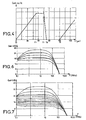
- TC1 must be equal, in absolute value, at each instant, to TC2, but of opposite sign, while TC3 must be equal in absolute value to TC4, but of opposite sign.
- TC3 and TC4 must have a maximum absolute value at time t o , which corresponds to the minimum capacity of varicaps 44 and 45.
- the voltages TC1 and TC2 must have a minimum absolute value, which corresponds to a maximum capacity for varicaps 26 and 33.
- only one control circuit for all the variable gain amplifiers of an ultrasonic ultrasound machine which may typically include 64 or 128 such amplifiers.
- FIG 5 the diagram of an exemplary embodiment of a control circuit 56 capable of supplying the voltages TC1 to TC4 from a single control voltage supplied by a generator 57 (comprising, in a manner known per se, a programmable digital generator and a digital-to-analog converter).
- the generator 57 directly drives a control stage comprising two operational amplifiers 58, 59 supplying the voltages TC1 and TC2, and via an auxiliary operational amplifier 60, a second control stage comprising the operational amplifiers 61, 62, which provide the voltages TC3 and TC4.
- All operational amplifiers 58 to 62 are mounted in the same way: their non-inverting input is connected to ground, their input
- the inverter is driven via a series resistor RS and a feedback resistor RCR, and they are powered symmetrically, each being connected to a positive voltage V + and a negative voltage V-, with respect to ground.
- the inverting input of the amplifier 61 is connected to ground by a resistor 63 in series with an auxiliary voltage source 64.
- the capacitances of the varicap diodes 44 and 45 vary between 12 pF and 36 pF, whereas those of the diodes 26 and 33 vary between 3 and 9 pF, for voltages TC1 to TC4 varying between 0 V and 4.3. V about.
- the ratio between the highest capacitance and the lowest capacitance of the varicap diodes is 3, which makes it possible to realize the variable gain amplifiers in integrated technology, BICmos, for example.
- This figure shows that the usable frequency range (at 1 dB of attenuation) ranges between 2 and 15 MHz, and that the gain of the amplifier can vary between 16 and 27 dB.
- the varicap diodes are made as discrete components, their capacity can vary in larger proportions. One can easily achieve a ratio of 20, or even better, with such discrete components. This, of course, results in a wider range of gain variation for the amplifier of the invention.
- figure 7 similar to figure 6
- the capacity of the diodes 44 and 45 varies from 6 to 120 pF, while that of the diodes 26 and 33 varies between 3 and 60 pF. It shows that the usable frequency range, at 1 dB of attenuation, extends between 2 and 8 MHz approximately, the gain varying between 11 and 35 dB.
Landscapes
- Engineering & Computer Science (AREA)
- Power Engineering (AREA)
- Amplifiers (AREA)
- Ultra Sonic Daignosis Equipment (AREA)
- Control Of Amplification And Gain Control (AREA)
- Investigating Or Analyzing Materials By The Use Of Ultrasonic Waves (AREA)
Claims (4)
- Rauscharme Verstärkervorrichtung mit variabler Verstärkung für Eingangssignale mit einem Dynamikumfang von über 100 dB, die mit einer Quelle von zu verstärkenden Signalen vom Typ Operationsverstärker (2) verbunden ist, deren Ausgang durch ein erstes reaktives Element (Z1) mit einem ihrer Eingänge verbunden ist, wobei dieser Eingang ferner durch ein zweites reaktives Element (Z2) mit einem gemeinsamen Stromversorgungspol des Verstärkers verbunden ist, wobei der Operationsverstärker einen einzelnen Verstärker (7, 13) umfasst und sein Eingang, mit dem die zwei reaktiven Elemente verbunden sind, sein invertierender Eingang ist, und wobei sein nicht invertierender Eingang mit der Quelle von zu verstärkenden Signalen verbunden ist und wobei die zwei reaktiven Elemente Elemente mit variabler Kapazität (9, 10) sind, dadurch gekennzeichnet, dass
jedes Element mit variabler Kapazität mindestens zwei in entgegengesetzten Richtungen montierte Kapazitätsdioden (26 und 33, 44 und 45) umfasst, die jeweils durch ihre eigene Steuerspannung (TC1 bis TC4) gesteuert werden, wobei diese Steuerspannungen sich in Bezug auf ein Bezugspotential symmetrisch verändern. - Verstärkervorrichtung nach Anspruch 1, dadurch gekennzeichnet, dass sie in Form einer anwendungsspezifischen integrierten Schaltung ausgebildet ist.
- Verstärkervorrichtung nach Anspruch 2, dadurch gekennzeichnet, dass sie in BiCMOS-Technologie hergestellt ist, wobei die Kapazitätsdioden ebenfalls integriert sind.
- Verstärkervorrichtung nach Anspruch 2, dadurch gekennzeichnet, dass nur die Kapazitätsdioden in Form von diskreten Komponenten ausgebildet sind.
Applications Claiming Priority (3)
| Application Number | Priority Date | Filing Date | Title |
|---|---|---|---|
| FR0205577A FR2839400A1 (fr) | 2002-05-03 | 2002-05-03 | Amplificateur a gain variable et faible bruit a grande dynamique |
| FR0205577 | 2002-05-03 | ||
| PCT/FR2003/001363 WO2003096528A2 (fr) | 2002-05-03 | 2003-04-30 | Montage amplificateur a gain variable et faible bruit a grande dynamique |
Publications (2)
| Publication Number | Publication Date |
|---|---|
| EP1502353A2 EP1502353A2 (de) | 2005-02-02 |
| EP1502353B1 true EP1502353B1 (de) | 2013-10-02 |
Family
ID=29226180
Family Applications (1)
| Application Number | Title | Priority Date | Filing Date |
|---|---|---|---|
| EP03740687.3A Expired - Lifetime EP1502353B1 (de) | 2002-05-03 | 2003-04-30 | Rauscharmer verstärker mit variabler verstärkung und hoher dynamik |
Country Status (6)
| Country | Link |
|---|---|
| EP (1) | EP1502353B1 (de) |
| JP (1) | JP2005529513A (de) |
| KR (1) | KR20050025169A (de) |
| FR (1) | FR2839400A1 (de) |
| NO (1) | NO20045317L (de) |
| WO (1) | WO2003096528A2 (de) |
Family Cites Families (3)
| Publication number | Priority date | Publication date | Assignee | Title |
|---|---|---|---|---|
| DE1907579B2 (de) * | 1969-02-14 | 1972-11-02 | Siemens AG, 1000 Berlin u. 8000 München | Regelbarer, gegengekoppelter verstaerker |
| JPH0774560A (ja) * | 1993-04-28 | 1995-03-17 | Night Technol Internatl | 音響システム用利得/等化回路 |
| JP3822010B2 (ja) * | 1999-12-01 | 2006-09-13 | アルプス電気株式会社 | 高周波増幅回路 |
-
2002
- 2002-05-03 FR FR0205577A patent/FR2839400A1/fr active Pending
-
2003
- 2003-04-30 KR KR1020047017663A patent/KR20050025169A/ko not_active Withdrawn
- 2003-04-30 JP JP2004504377A patent/JP2005529513A/ja active Pending
- 2003-04-30 WO PCT/FR2003/001363 patent/WO2003096528A2/fr not_active Ceased
- 2003-04-30 EP EP03740687.3A patent/EP1502353B1/de not_active Expired - Lifetime
-
2004
- 2004-12-03 NO NO20045317A patent/NO20045317L/no unknown
Also Published As
| Publication number | Publication date |
|---|---|
| WO2003096528A3 (fr) | 2004-08-19 |
| JP2005529513A (ja) | 2005-09-29 |
| KR20050025169A (ko) | 2005-03-11 |
| WO2003096528A2 (fr) | 2003-11-20 |
| NO20045317L (no) | 2004-12-03 |
| FR2839400A1 (fr) | 2003-11-07 |
| EP1502353A2 (de) | 2005-02-02 |
Similar Documents
| Publication | Publication Date | Title |
|---|---|---|
| FR2633467A1 (fr) | Multiplicateur de frequence a rang de multiplication programmable | |
| EP0414328B1 (de) | Differenzverstärker mit Kondensatorkopplung | |
| EP0060165A1 (de) | In Frequenz gesteuerter Oszillator mit einem piezoelektrischen Element und der ein gedehntes Frequenzänderungsgebiet hat | |
| EP2131494B1 (de) | Schaltkreis mit geschalteten Kapazitäten mit geringem Energieverbrauch | |
| EP0810728B1 (de) | Analoger Tonfilter für hohe Frequenzen | |
| FR2958095A1 (fr) | Circuit passe-bas du second ordre | |
| FR2514214A1 (fr) | Circuit a gain variable | |
| FR2529411A1 (fr) | Amplificateur de courant a circuit integre avec amelioration de la linearite et la precision du coefficient de multiplication du circuit | |
| EP2037218A2 (de) | Elektronischer Schaltkreis zur Messung eines physischen Parameters, der ein analoges Messsignal liefert, das von der angelegten Spannung abhängt | |
| EP0564341B1 (de) | Videoverstärker mit Verstärkungs- und Ausrichtsteuerung | |
| EP0201964B1 (de) | Verstärker für Hochfrequenzen | |
| EP0401906B1 (de) | Phasenschieber | |
| FR2661290A1 (fr) | Amplificateur de puissance notamment pour signaux carres. | |
| EP1362417B1 (de) | Verstärker mit symmetrischen ein- und ausgängen und mit variabler verstärkung | |
| EP1502353A2 (de) | Rauscharmer verstärker mit variabler verstärkung und hoher dynamik | |
| FR2563168A1 (fr) | Circuit perfectionne d'entree pour une unite de reglage electronique de la vitesse d'un vehicule | |
| FR2581275A1 (fr) | Recepteur de signaux optiques a tres large bande. | |
| EP0413644B1 (de) | Vergleichsschaltung für in Amplitude modulierte Hochfrequenzsignale | |
| EP1762854A2 (de) | Messvorrichtung für sehr kurze Stromimpulse | |
| FR2477340A1 (fr) | Circuit amplificateur dont l'amplification totale peut etre commandee par une tension de commande | |
| EP0083529A2 (de) | Verstärkereinrichtung für stark schwankende Spannungen und Spannungsquelle mit einer derartigen Verstärkereinrichtung | |
| EP0645884A1 (de) | Verstärkerkette in Strommode, Operationsverstärker, Verstärkungszelle und zugehöriges Verstärkerelement | |
| EP0506186A1 (de) | Videoverstärkervorrichtung | |
| EP0577474B1 (de) | Weckschaltung für einen Telefonapparat | |
| EP1569332B1 (de) | Leistungsverstärker und Operationsverstärker, der diesen beinhaltet |
Legal Events
| Date | Code | Title | Description |
|---|---|---|---|
| PUAI | Public reference made under article 153(3) epc to a published international application that has entered the european phase |
Free format text: ORIGINAL CODE: 0009012 |
|
| 17P | Request for examination filed |
Effective date: 20041021 |
|
| AK | Designated contracting states |
Kind code of ref document: A2 Designated state(s): AT BE BG CH CY CZ DE DK EE ES FI FR GB GR HU IE IT LI LU MC NL PT RO SE SI SK TR |
|
| 17Q | First examination report despatched |
Effective date: 20080513 |
|
| GRAP | Despatch of communication of intention to grant a patent |
Free format text: ORIGINAL CODE: EPIDOSNIGR1 |
|
| INTG | Intention to grant announced |
Effective date: 20130430 |
|
| GRAS | Grant fee paid |
Free format text: ORIGINAL CODE: EPIDOSNIGR3 |
|
| GRAA | (expected) grant |
Free format text: ORIGINAL CODE: 0009210 |
|
| AK | Designated contracting states |
Kind code of ref document: B1 Designated state(s): AT BE BG CH CY CZ DE DK EE ES FI FR GB GR HU IE IT LI LU MC NL PT RO SE SI SK TR |
|
| REG | Reference to a national code |
Ref country code: GB Ref legal event code: FG4D Free format text: NOT ENGLISH |
|
| REG | Reference to a national code |
Ref country code: CH Ref legal event code: EP Ref country code: AT Ref legal event code: REF Ref document number: 635045 Country of ref document: AT Kind code of ref document: T Effective date: 20131015 |
|
| REG | Reference to a national code |
Ref country code: IE Ref legal event code: FG4D Free format text: LANGUAGE OF EP DOCUMENT: FRENCH |
|
| REG | Reference to a national code |
Ref country code: DE Ref legal event code: R096 Ref document number: 60345015 Country of ref document: DE Effective date: 20131128 |
|
| REG | Reference to a national code |
Ref country code: NL Ref legal event code: T3 |
|
| REG | Reference to a national code |
Ref country code: AT Ref legal event code: MK05 Ref document number: 635045 Country of ref document: AT Kind code of ref document: T Effective date: 20131002 |
|
| PG25 | Lapsed in a contracting state [announced via postgrant information from national office to epo] |
Ref country code: SI Free format text: LAPSE BECAUSE OF FAILURE TO SUBMIT A TRANSLATION OF THE DESCRIPTION OR TO PAY THE FEE WITHIN THE PRESCRIBED TIME-LIMIT Effective date: 20131002 |
|
| PG25 | Lapsed in a contracting state [announced via postgrant information from national office to epo] |
Ref country code: SE Free format text: LAPSE BECAUSE OF FAILURE TO SUBMIT A TRANSLATION OF THE DESCRIPTION OR TO PAY THE FEE WITHIN THE PRESCRIBED TIME-LIMIT Effective date: 20131002 Ref country code: CZ Free format text: LAPSE BECAUSE OF FAILURE TO SUBMIT A TRANSLATION OF THE DESCRIPTION OR TO PAY THE FEE WITHIN THE PRESCRIBED TIME-LIMIT Effective date: 20131002 Ref country code: FI Free format text: LAPSE BECAUSE OF FAILURE TO SUBMIT A TRANSLATION OF THE DESCRIPTION OR TO PAY THE FEE WITHIN THE PRESCRIBED TIME-LIMIT Effective date: 20131002 |
|
| PG25 | Lapsed in a contracting state [announced via postgrant information from national office to epo] |
Ref country code: AT Free format text: LAPSE BECAUSE OF FAILURE TO SUBMIT A TRANSLATION OF THE DESCRIPTION OR TO PAY THE FEE WITHIN THE PRESCRIBED TIME-LIMIT Effective date: 20131002 Ref country code: ES Free format text: LAPSE BECAUSE OF FAILURE TO SUBMIT A TRANSLATION OF THE DESCRIPTION OR TO PAY THE FEE WITHIN THE PRESCRIBED TIME-LIMIT Effective date: 20131002 Ref country code: CY Free format text: LAPSE BECAUSE OF FAILURE TO SUBMIT A TRANSLATION OF THE DESCRIPTION OR TO PAY THE FEE WITHIN THE PRESCRIBED TIME-LIMIT Effective date: 20131002 |
|
| PG25 | Lapsed in a contracting state [announced via postgrant information from national office to epo] |
Ref country code: PT Free format text: LAPSE BECAUSE OF FAILURE TO SUBMIT A TRANSLATION OF THE DESCRIPTION OR TO PAY THE FEE WITHIN THE PRESCRIBED TIME-LIMIT Effective date: 20140203 |
|
| REG | Reference to a national code |
Ref country code: DE Ref legal event code: R097 Ref document number: 60345015 Country of ref document: DE |
|
| PG25 | Lapsed in a contracting state [announced via postgrant information from national office to epo] |
Ref country code: EE Free format text: LAPSE BECAUSE OF FAILURE TO SUBMIT A TRANSLATION OF THE DESCRIPTION OR TO PAY THE FEE WITHIN THE PRESCRIBED TIME-LIMIT Effective date: 20131002 |
|
| PLBE | No opposition filed within time limit |
Free format text: ORIGINAL CODE: 0009261 |
|
| STAA | Information on the status of an ep patent application or granted ep patent |
Free format text: STATUS: NO OPPOSITION FILED WITHIN TIME LIMIT |
|
| PG25 | Lapsed in a contracting state [announced via postgrant information from national office to epo] |
Ref country code: SK Free format text: LAPSE BECAUSE OF FAILURE TO SUBMIT A TRANSLATION OF THE DESCRIPTION OR TO PAY THE FEE WITHIN THE PRESCRIBED TIME-LIMIT Effective date: 20131002 Ref country code: RO Free format text: LAPSE BECAUSE OF FAILURE TO SUBMIT A TRANSLATION OF THE DESCRIPTION OR TO PAY THE FEE WITHIN THE PRESCRIBED TIME-LIMIT Effective date: 20131002 |
|
| 26N | No opposition filed |
Effective date: 20140703 |
|
| PG25 | Lapsed in a contracting state [announced via postgrant information from national office to epo] |
Ref country code: DK Free format text: LAPSE BECAUSE OF FAILURE TO SUBMIT A TRANSLATION OF THE DESCRIPTION OR TO PAY THE FEE WITHIN THE PRESCRIBED TIME-LIMIT Effective date: 20131002 |
|
| REG | Reference to a national code |
Ref country code: DE Ref legal event code: R097 Ref document number: 60345015 Country of ref document: DE Effective date: 20140703 |
|
| PG25 | Lapsed in a contracting state [announced via postgrant information from national office to epo] |
Ref country code: MC Free format text: LAPSE BECAUSE OF FAILURE TO SUBMIT A TRANSLATION OF THE DESCRIPTION OR TO PAY THE FEE WITHIN THE PRESCRIBED TIME-LIMIT Effective date: 20131002 Ref country code: LU Free format text: LAPSE BECAUSE OF FAILURE TO SUBMIT A TRANSLATION OF THE DESCRIPTION OR TO PAY THE FEE WITHIN THE PRESCRIBED TIME-LIMIT Effective date: 20140430 |
|
| REG | Reference to a national code |
Ref country code: CH Ref legal event code: PL |
|
| PG25 | Lapsed in a contracting state [announced via postgrant information from national office to epo] |
Ref country code: CH Free format text: LAPSE BECAUSE OF NON-PAYMENT OF DUE FEES Effective date: 20140430 Ref country code: LI Free format text: LAPSE BECAUSE OF NON-PAYMENT OF DUE FEES Effective date: 20140430 |
|
| REG | Reference to a national code |
Ref country code: FR Ref legal event code: CD Owner name: TUX ULTRASOUND SAS, FR Effective date: 20150109 Ref country code: FR Ref legal event code: CA Effective date: 20150109 |
|
| REG | Reference to a national code |
Ref country code: FR Ref legal event code: PLFP Year of fee payment: 14 |
|
| PG25 | Lapsed in a contracting state [announced via postgrant information from national office to epo] |
Ref country code: BG Free format text: LAPSE BECAUSE OF FAILURE TO SUBMIT A TRANSLATION OF THE DESCRIPTION OR TO PAY THE FEE WITHIN THE PRESCRIBED TIME-LIMIT Effective date: 20131002 |
|
| PG25 | Lapsed in a contracting state [announced via postgrant information from national office to epo] |
Ref country code: GR Free format text: LAPSE BECAUSE OF FAILURE TO SUBMIT A TRANSLATION OF THE DESCRIPTION OR TO PAY THE FEE WITHIN THE PRESCRIBED TIME-LIMIT Effective date: 20140103 |
|
| PG25 | Lapsed in a contracting state [announced via postgrant information from national office to epo] |
Ref country code: TR Free format text: LAPSE BECAUSE OF FAILURE TO SUBMIT A TRANSLATION OF THE DESCRIPTION OR TO PAY THE FEE WITHIN THE PRESCRIBED TIME-LIMIT Effective date: 20131002 Ref country code: HU Free format text: LAPSE BECAUSE OF FAILURE TO SUBMIT A TRANSLATION OF THE DESCRIPTION OR TO PAY THE FEE WITHIN THE PRESCRIBED TIME-LIMIT; INVALID AB INITIO Effective date: 20030430 Ref country code: BE Free format text: LAPSE BECAUSE OF FAILURE TO SUBMIT A TRANSLATION OF THE DESCRIPTION OR TO PAY THE FEE WITHIN THE PRESCRIBED TIME-LIMIT Effective date: 20140430 |
|
| REG | Reference to a national code |
Ref country code: FR Ref legal event code: PLFP Year of fee payment: 15 |
|
| REG | Reference to a national code |
Ref country code: FR Ref legal event code: PLFP Year of fee payment: 16 |
|
| PGFP | Annual fee paid to national office [announced via postgrant information from national office to epo] |
Ref country code: IE Payment date: 20220323 Year of fee payment: 20 Ref country code: GB Payment date: 20220323 Year of fee payment: 20 |
|
| PGFP | Annual fee paid to national office [announced via postgrant information from national office to epo] |
Ref country code: NL Payment date: 20220330 Year of fee payment: 20 Ref country code: FR Payment date: 20220321 Year of fee payment: 20 |
|
| PGFP | Annual fee paid to national office [announced via postgrant information from national office to epo] |
Ref country code: IT Payment date: 20220328 Year of fee payment: 20 Ref country code: DE Payment date: 20220322 Year of fee payment: 20 |
|
| REG | Reference to a national code |
Ref country code: DE Ref legal event code: R071 Ref document number: 60345015 Country of ref document: DE |
|
| REG | Reference to a national code |
Ref country code: NL Ref legal event code: MK Effective date: 20230429 |
|
| REG | Reference to a national code |
Ref country code: IE Ref legal event code: MK9A Ref country code: GB Ref legal event code: PE20 Expiry date: 20230429 |
|
| PG25 | Lapsed in a contracting state [announced via postgrant information from national office to epo] |
Ref country code: IE Free format text: LAPSE BECAUSE OF EXPIRATION OF PROTECTION Effective date: 20230430 |
|
| PG25 | Lapsed in a contracting state [announced via postgrant information from national office to epo] |
Ref country code: GB Free format text: LAPSE BECAUSE OF EXPIRATION OF PROTECTION Effective date: 20230429 |