EP1501337A1 - Organic electroluminescence device and material thereof - Google Patents
Organic electroluminescence device and material thereof Download PDFInfo
- Publication number
- EP1501337A1 EP1501337A1 EP03725696A EP03725696A EP1501337A1 EP 1501337 A1 EP1501337 A1 EP 1501337A1 EP 03725696 A EP03725696 A EP 03725696A EP 03725696 A EP03725696 A EP 03725696A EP 1501337 A1 EP1501337 A1 EP 1501337A1
- Authority
- EP
- European Patent Office
- Prior art keywords
- compound
- organic electroluminescence
- electroluminescence device
- layer
- group
- Prior art date
- Legal status (The legal status is an assumption and is not a legal conclusion. Google has not performed a legal analysis and makes no representation as to the accuracy of the status listed.)
- Granted
Links
- 0 CCCCC(CC1)CCC1C(C)CC* Chemical compound CCCCC(CC1)CCC1C(C)CC* 0.000 description 4
- YXFVVABEGXRONW-UHFFFAOYSA-N Cc1ccccc1 Chemical compound Cc1ccccc1 YXFVVABEGXRONW-UHFFFAOYSA-N 0.000 description 1
Images

Classifications
-
- C—CHEMISTRY; METALLURGY
- C09—DYES; PAINTS; POLISHES; NATURAL RESINS; ADHESIVES; COMPOSITIONS NOT OTHERWISE PROVIDED FOR; APPLICATIONS OF MATERIALS NOT OTHERWISE PROVIDED FOR
- C09K—MATERIALS FOR MISCELLANEOUS APPLICATIONS, NOT PROVIDED FOR ELSEWHERE
- C09K11/00—Luminescent materials, e.g. electroluminescent or chemiluminescent
- C09K11/06—Luminescent materials, e.g. electroluminescent or chemiluminescent containing organic luminescent materials
-
- H—ELECTRICITY
- H10—SEMICONDUCTOR DEVICES; ELECTRIC SOLID-STATE DEVICES NOT OTHERWISE PROVIDED FOR
- H10K—ORGANIC ELECTRIC SOLID-STATE DEVICES
- H10K71/00—Manufacture or treatment specially adapted for the organic devices covered by this subclass
- H10K71/30—Doping active layers, e.g. electron transporting layers
-
- H—ELECTRICITY
- H10—SEMICONDUCTOR DEVICES; ELECTRIC SOLID-STATE DEVICES NOT OTHERWISE PROVIDED FOR
- H10K—ORGANIC ELECTRIC SOLID-STATE DEVICES
- H10K85/00—Organic materials used in the body or electrodes of devices covered by this subclass
- H10K85/60—Organic compounds having low molecular weight
-
- H—ELECTRICITY
- H10—SEMICONDUCTOR DEVICES; ELECTRIC SOLID-STATE DEVICES NOT OTHERWISE PROVIDED FOR
- H10K—ORGANIC ELECTRIC SOLID-STATE DEVICES
- H10K85/00—Organic materials used in the body or electrodes of devices covered by this subclass
- H10K85/60—Organic compounds having low molecular weight
- H10K85/615—Polycyclic condensed aromatic hydrocarbons, e.g. anthracene
-
- H—ELECTRICITY
- H10—SEMICONDUCTOR DEVICES; ELECTRIC SOLID-STATE DEVICES NOT OTHERWISE PROVIDED FOR
- H10K—ORGANIC ELECTRIC SOLID-STATE DEVICES
- H10K2102/00—Constructional details relating to the organic devices covered by this subclass
- H10K2102/10—Transparent electrodes, e.g. using graphene
- H10K2102/101—Transparent electrodes, e.g. using graphene comprising transparent conductive oxides [TCO]
- H10K2102/103—Transparent electrodes, e.g. using graphene comprising transparent conductive oxides [TCO] comprising indium oxides, e.g. ITO
-
- H—ELECTRICITY
- H10—SEMICONDUCTOR DEVICES; ELECTRIC SOLID-STATE DEVICES NOT OTHERWISE PROVIDED FOR
- H10K—ORGANIC ELECTRIC SOLID-STATE DEVICES
- H10K50/00—Organic light-emitting devices
- H10K50/10—OLEDs or polymer light-emitting diodes [PLED]
- H10K50/11—OLEDs or polymer light-emitting diodes [PLED] characterised by the electroluminescent [EL] layers
-
- H—ELECTRICITY
- H10—SEMICONDUCTOR DEVICES; ELECTRIC SOLID-STATE DEVICES NOT OTHERWISE PROVIDED FOR
- H10K—ORGANIC ELECTRIC SOLID-STATE DEVICES
- H10K50/00—Organic light-emitting devices
- H10K50/10—OLEDs or polymer light-emitting diodes [PLED]
- H10K50/14—Carrier transporting layers
-
- H—ELECTRICITY
- H10—SEMICONDUCTOR DEVICES; ELECTRIC SOLID-STATE DEVICES NOT OTHERWISE PROVIDED FOR
- H10K—ORGANIC ELECTRIC SOLID-STATE DEVICES
- H10K50/00—Organic light-emitting devices
- H10K50/10—OLEDs or polymer light-emitting diodes [PLED]
- H10K50/17—Carrier injection layers
-
- H—ELECTRICITY
- H10—SEMICONDUCTOR DEVICES; ELECTRIC SOLID-STATE DEVICES NOT OTHERWISE PROVIDED FOR
- H10K—ORGANIC ELECTRIC SOLID-STATE DEVICES
- H10K50/00—Organic light-emitting devices
- H10K50/10—OLEDs or polymer light-emitting diodes [PLED]
- H10K50/17—Carrier injection layers
- H10K50/171—Electron injection layers
-
- H—ELECTRICITY
- H10—SEMICONDUCTOR DEVICES; ELECTRIC SOLID-STATE DEVICES NOT OTHERWISE PROVIDED FOR
- H10K—ORGANIC ELECTRIC SOLID-STATE DEVICES
- H10K85/00—Organic materials used in the body or electrodes of devices covered by this subclass
- H10K85/10—Organic polymers or oligomers
- H10K85/111—Organic polymers or oligomers comprising aromatic, heteroaromatic, or aryl chains, e.g. polyaniline, polyphenylene or polyphenylene vinylene
-
- H—ELECTRICITY
- H10—SEMICONDUCTOR DEVICES; ELECTRIC SOLID-STATE DEVICES NOT OTHERWISE PROVIDED FOR
- H10K—ORGANIC ELECTRIC SOLID-STATE DEVICES
- H10K85/00—Organic materials used in the body or electrodes of devices covered by this subclass
- H10K85/10—Organic polymers or oligomers
- H10K85/141—Organic polymers or oligomers comprising aliphatic or olefinic chains, e.g. poly N-vinylcarbazol, PVC or PTFE
- H10K85/146—Organic polymers or oligomers comprising aliphatic or olefinic chains, e.g. poly N-vinylcarbazol, PVC or PTFE poly N-vinylcarbazol; Derivatives thereof
-
- H—ELECTRICITY
- H10—SEMICONDUCTOR DEVICES; ELECTRIC SOLID-STATE DEVICES NOT OTHERWISE PROVIDED FOR
- H10K—ORGANIC ELECTRIC SOLID-STATE DEVICES
- H10K85/00—Organic materials used in the body or electrodes of devices covered by this subclass
- H10K85/30—Coordination compounds
- H10K85/321—Metal complexes comprising a group IIIA element, e.g. Tris (8-hydroxyquinoline) gallium [Gaq3]
- H10K85/324—Metal complexes comprising a group IIIA element, e.g. Tris (8-hydroxyquinoline) gallium [Gaq3] comprising aluminium, e.g. Alq3
-
- H—ELECTRICITY
- H10—SEMICONDUCTOR DEVICES; ELECTRIC SOLID-STATE DEVICES NOT OTHERWISE PROVIDED FOR
- H10K—ORGANIC ELECTRIC SOLID-STATE DEVICES
- H10K85/00—Organic materials used in the body or electrodes of devices covered by this subclass
- H10K85/60—Organic compounds having low molecular weight
- H10K85/615—Polycyclic condensed aromatic hydrocarbons, e.g. anthracene
- H10K85/626—Polycyclic condensed aromatic hydrocarbons, e.g. anthracene containing more than one polycyclic condensed aromatic rings, e.g. bis-anthracene
-
- Y—GENERAL TAGGING OF NEW TECHNOLOGICAL DEVELOPMENTS; GENERAL TAGGING OF CROSS-SECTIONAL TECHNOLOGIES SPANNING OVER SEVERAL SECTIONS OF THE IPC; TECHNICAL SUBJECTS COVERED BY FORMER USPC CROSS-REFERENCE ART COLLECTIONS [XRACs] AND DIGESTS
- Y10—TECHNICAL SUBJECTS COVERED BY FORMER USPC
- Y10S—TECHNICAL SUBJECTS COVERED BY FORMER USPC CROSS-REFERENCE ART COLLECTIONS [XRACs] AND DIGESTS
- Y10S428/00—Stock material or miscellaneous articles
- Y10S428/917—Electroluminescent
Definitions
- the present invention relates to an organic electroluminescence device and a material thereof. More particularly, the present invention relates to an organic electroluminescence device that emits light upon application of voltage to its emission layer of an organic compound and relates also to a charge transport material incorporated thereinto.
- Tang et al. searched for the optimal electrode and organic compound that would increase the emission efficiency of the device. They prepared an organic electroluminescence device in which the hole transport layer is an aromatic amine compound and the electron transport emission layer is an aluminum complex of 8-hydoxyquinoline. This device emits light when it has DC voltage applied across its electrodes. The DC voltage injects holes through the anode and electrons through the cathode, so that they undergo recombination in the emission layer to emit light.
- hole transport materials are aromatic diamine derivatives (disclosed in Japanese Patent Laid-open Nos. Hei 8-20771, Hei 8-40995, and Hei 8-40997) and aromatic amine-containing polymers (disclosed in Japanese Patent Laid-open Nos. Hei 11-283750 and 2000-36390).
- the existing organic electroluminescence devices have some problems to be addressed. That is, they need to have a longer life, to work at a lower driving voltage, and to work with a constant current without voltage increase and luminance decrease. Although no elucidation has been made yet, the performance of the device seems to depend on the properties (such as glass transition temperature and melting point) of the organic materials constituting the device. The device made of an organic material poor in heat resistance tends to break during continuous operation.
- Any device with a short life or a high driving voltage poses a problem when used as the light source for facsimile, copying machine, and back light of liquid crystal display, particularly, the device is not desirable for display.
- the present inventors conducted a series of researches to tackle the above-mentioned problems. As a result, they found the organic electroluminescence device and the material to be used therefor, which are defined in the present invention.
- layer containing a compound with carbenium ions shall mean a charge transport layer, which includes, for example, electron injection layer, electron transport layer, hole transport layer, and hole injection layer.
- This material is a charge transfer material that forms the above-mentioned layers. It includes, for example, electron injection material, electron transport material, hole injection material, and hole transport material. The one for hole transport and hole injection is preferable.
- the organic electroluminescence device is one which has one or more than one emission layer in the form of thin film of an organic compound between paired electrodes. It is characterized in having at least one layer containing a compound with carbenium ions. This layer may be a hole transport layer, hole injection layer, electron transport layer, or electron injection layer, for example.
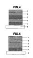
- Figs. 1 to 5 are schematic diagrams illustrating the structure of the device and are not intended to restrict the scope of the present invention.
- Figs. 1 to 5 are schematic diagrams illustrating the embodiments of the organic electroluminescence device according to the present invention.
- a cathode 1 an emission layer 2, a hole transport layer 3, an anode 4, a substrate 5, a hole injection layer 6, an electron injection layer 7, and an electron transport layer 8.
- the layer of organic compound held between paired electrodes is composed of an emission layer and at least one charge transport layer (such as electron injection layer, electron transport layer, hole transport layer, and hole injection layer).
- at least one of the charge transport layers should contain a compound with carbenium ions.
- the charge transport layer containing a compound with carbenium ions improves the efficiency of electron and hole injection into the emission layer, thereby permitting the organic electroluminescence device to emit light at a low voltage.
- the layer containing a compound with carbenium ions should be used as a hole transport layer 3, so that the efficiency of hole injection into the emission layer 2 improves and the organic electroluminescence device emits light at a low voltage.
- the layer containing a compound with carbenium ions should be used as both of a hole transport layer 3 and a hole injection layer 6, or either of a hole transport layer 3 or a hole injection layer 6, as shown in Figs. 2 and 3, so that the efficiency of hole injection into the emission layer 2 improves and the organic electroluminescence device emits light at a low voltage.
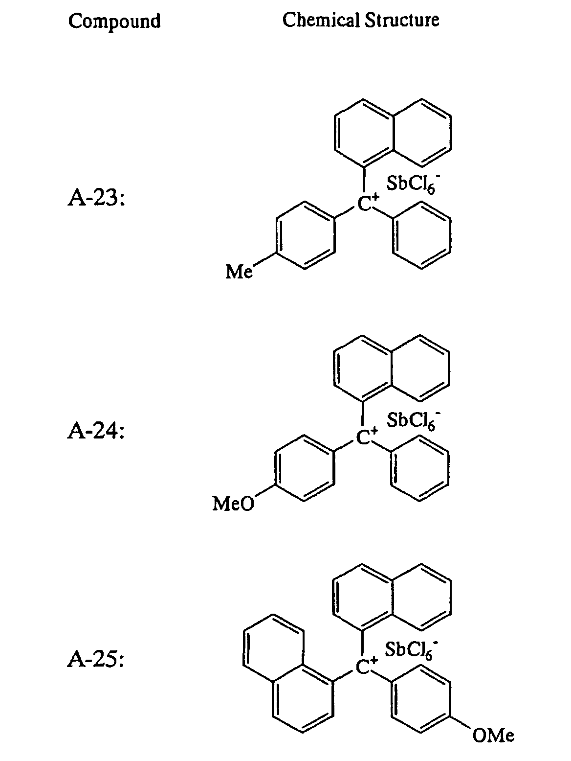
- the compound with carbenium ions is one which is represented by the formula (1) below.
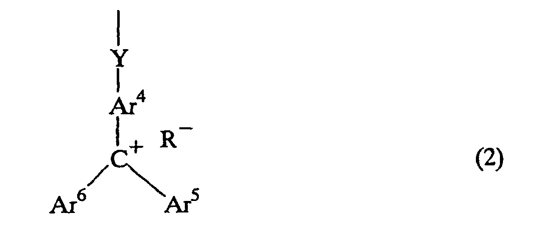
- Ar 1 to Ar 3 denote identical or different, substituted or unsubstituted aromatic groups, with at least one of them being a monovalent substituent group represented by the formula (2) below.
- Ar 4 to Ar 6 denote substituted or unsubstituted aromatic groups which are identical with or different from Ar 1 to Ar 3 , respectively;
- Y denotes a single bond, -O-, or a divalent organic group selected from C 1-6 alkylene group, -COO-, -CONH-, 9H-fluorenylene group, and 9,9-dimethyl-9H-flurorenylene group; and
- R - denotes an anion species.
- Ar 1 to Ar 6 may be identical or different, substituted or unsubstituted aromatic groups.
- Unsubstituted aromatic groups include, for example, phenyl group, biphenyl group, triphenyl group, tetraphenyl group, naphthyl group, phenanthrenyl group, fluorenyl group, and anthranyl group.
- the substituted aromatic group mentioned above has any of the following substituent groups.
- electron-donating groups which include C 1-4 alkyl groups, such as methyl group, ethyl group, propyl group, isopropyl group, butyl group, isobutyl group, s-butyl group, and t-butyl group; C 1-4 alkoxy groups, such as methoxy group, ethoxy group, propoxy group, isopropoxy group, butoxy group, isobutoxy group, s-butoxy group, and t-butoxy group; and amino groups, methylamino groups, dimethylamino groups, ethylamino groups, and diethylamino groups.
- the number of these substituent groups is usually 1 to 3.
- aromatic groups Ar 1 to Ar 6 include phenyl groups, o-, m-, and p-tolyl groups, xylyl groups, o-, m-, and p-cumenyl groups, biphenyl groups, naphthyl groups, 4-methoxy-phenyl groups, 9H-fluorenyl groups, and 9,9-dimethyl-9H-flurorenyl groups.
- Y in the substituent group denotes a single bond, -O-, or a divalent organic group selected from C 1-6 alkylene group, -COO-, -CONH-, 9H-fluorenylene group, and 9,9-dimethyl-9H-flurorenylene group.
- the compound with carbenium cations includes an oligomer or a polymer in which the main chain has the structure of the formula (1), with the substituent groups represented by the formula (2) repeatedly binding to Ar 5 and Ar 6 . It also includes an oligomer or a polymer in which the side chains have the substituent groups represented by the formula (2).
- the carbenium cation represented in the formula (1) above has a counter ion indicated by R-.
- This anion includes, for example, SbX 6 - , PX 6 - , TaX 6 - , ClO 4 - , ReO 4 - , BX 4 - , AsX 6 - , and AlX 6 - .
- SbX 6 - is preferable (where X denotes a halogen atom).
- the halogen atom includes fluorine atom, chlorine atom, bromine atom, and iodine atom, with the former two being preferable.
- the compound represented by the formula (1) may be synthesized in any way without specific restrictions.
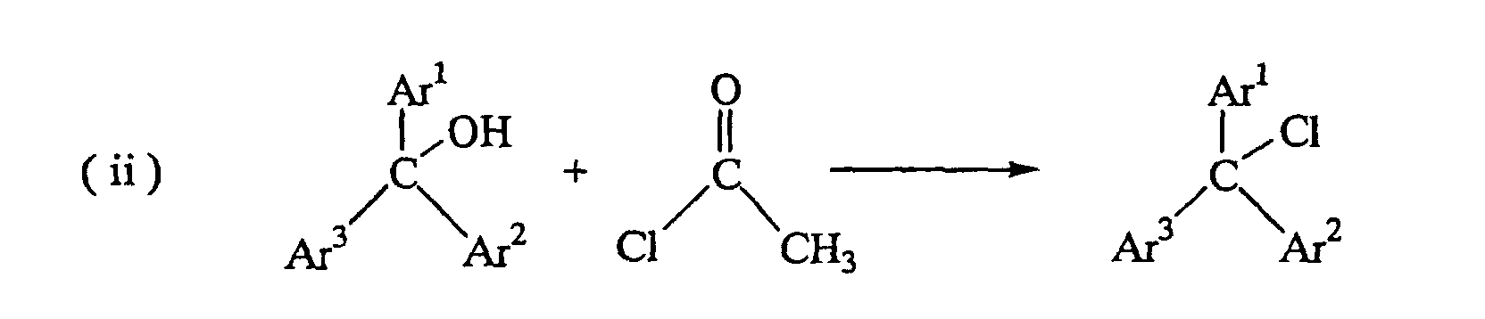
- the process for synthesis may consist of the following three steps, assuming that the anion is SbCl 6 - and Ar 1 is a mono-halogenated phenyl compound (X-Ar 1 , where X is Cl, Br, or I).
- a solvent such as THF
- the reaction temperature ranges from room temperature to 60°C, and the reaction time ranges from 3 hours to 7 hours. After acetyl chloride has been removed, there is obtained the desired triphenylchloromethane compound.
- triphenylchloromethane compounds are commercially available as reagents.
- the compound with carbenium ions may be used alone as the charge transport material, or the polymer containing a compound with carbenium ions in the main chain or side chain may be used alone as the charge transport material. More than one of such compounds or polymers may be used in combination with one another. Also, the compound with carbenium ions may be mixed with any other charge transport material. Alternatively, the compound with carbenium ions may be combined with a compound capable of charge transfer to form a polymer. Such materials may be used alone or in combination with one another.
- the layer containing carbenium ions may be formed by coating and ensuing drying (on a substrate or another layer) from a solvent solution containing a compound with carbenium ions. Coating may be accomplished by spin coating, printing, or the like.
- the solvent used for coating includes, for example, halogenated hydrocarbon solvents (such as chloroform, dichloromethane, dichloroethane, trichloroethylene, ethylene dichloride, tetrachloroethane, and chlorobenzene), aprotic polar solvents (such as N-methyl-2-pyrrolidone (NMP), dimethylformamide (DMF), dimethylacetamide (DMAc), and dimethylsulfoxide (DMSO)), and polar solvents (such as propylene glycol monobutyl ether, dipropylene glycol monomethyl ether, dipropylene glycol monoethyl ether, and other alkoxy alcohols).
- halogenated hydrocarbon solvents such as chloroform, dichloromethane, dichloroethane, trichloroethylene, ethylene dichloride, tetrachloroethane, and chlorobenzene
- aprotic polar solvents such as N-methyl-2-pyr
- the compound with carbenium ions may be used alone as the hole transport material. It may also be mixed with any other hole transport material for improvement in its characteristic properties.
- 1,1-bis(4-di-p-triphenylaminophenyl)cyclohexane which is an aromatic amine compound having a tertiary aromatic amine unit connected thereto.
- Aromatic triamine of starburst structure such as a derivative of trtiphenylbenzene. (USP No. 4923774)
- Aromatic diamine such as N,N'-diphenyl-N,N'-bis(3-methylphenyl)biphenyl-4,4'-diamine. (USP No. 4764625)
- Aromatic diamine composed of tertiary aromatic amine units connected through an ethylene group.
- Aromatic diamine with a styryl structure in which aromatic tertiary amine units are connected through a thiophene group Japanese Patent Laid-open No. Hei 4-3044666
- Triamine compound (Japanese Patent Laid-open No. Hei 5-239455) These materials may be used alone or in combination with one another.
- hole transport materials include polyvinylcarbazole, polysilane, polyphosphazene (Japanese Patent Laid-open No. Hei 5-310949), polyamide, polybiphenylamine, and polymer having a triphenylamine skeleton. These examples are not limitative. They may be used alone or in combination with one another.
- a compound with carbenium ions may be used alone as an electron transfer material, or it may be used in combination with another electron transfer material for improvement in its characteristic properties.
- Examples of other electron transfer materials include nitro-substituted fluorenone derivatives, nitro-substituted fluorene derivatives, thiopyran dioxide derivatives, diphenone derivatives, perylene tetracarboxyl derivatives, anthraquionodimethane derivatives, fluoronylidenemethane derivatives, perylene derivatives, oxadiazole derivative and polymers, quinoline derivatavies, triazole derivatives and polymers, and imidazole derivatives. These examples are not limitative. They may be used alone or in combination with one another.
- the anode 4 is a transparent electrode having a surface resistance of 1 to 50 ⁇ / ⁇ and a visible ray transmittance equal to or higher than 80%. It should preferably be a transparent film formed from indium-tin oxide (ITO) or zinc oxide-aluminum in amorphous form or microcrystalline form. Alternatively, it should preferably be a transparent film of laminate structure formed on the transparent insulating substrate 1 (such as glass and plastic film) by vacuum deposition or sputtering.
- ITO indium-tin oxide
- zinc oxide-aluminum in amorphous form or microcrystalline form.
- the transparent film of laminate structure is composed of a core layer (about 10 nm thick) of silver, chromium, copper, or copper-silver alloy (which serves to reduce resistance) and outer layers of ITO, titanium oxide, or tin oxide (in amorphous or microcrystalline form).
- the anode may also be a semi-transparent electrode having gold or platinum deposited thereon or a semi-transparent electrode having a polymer (such as polyaniline, polythiophene, and polypyrrole) coated thereon.
- the emission layer 2 is formed from any of aromatic amine compounds, coumarin compounds (as a laser dye), perylene derivatives, anthracene derivatives, rubrene derivatives, and tris(8-hydroxyquinoline)-aluminum metal complex.
- the cathode 1 is formed from any of metal (with a small work function), alloy thereof, electrically conductive compounds, and mixtures thereof. Examples of such metals include Na, K, Mg, Li, and In.
- the cathode may be formed by vacuum deposition or sputtering.
- a glass substrate with ITO was cleaned with a neutral detergent and then ultrasonically washed sequentially in water, acetone, and isopropanol. It further underwent boiling in isopropanol and UV-ozone cleaning. The organic layer and cathode were formed by vacuum deposition. Thus there was obtained the desired device.
- the hole transport material was commercial ⁇ -naphthylphenyldiamine ( ⁇ -NPD, purified by sublimation).
- ⁇ -NPD ⁇ -naphthylphenyldiamine
- the vacuum deposition for the hole transport material was carried out at a degree of vacuum no higher than 8 ⁇ 10 -4 Pa.
- the vacuum deposition was also carried out at a rate of 0.3 nm/s until the deposited film became 50 nm thick.
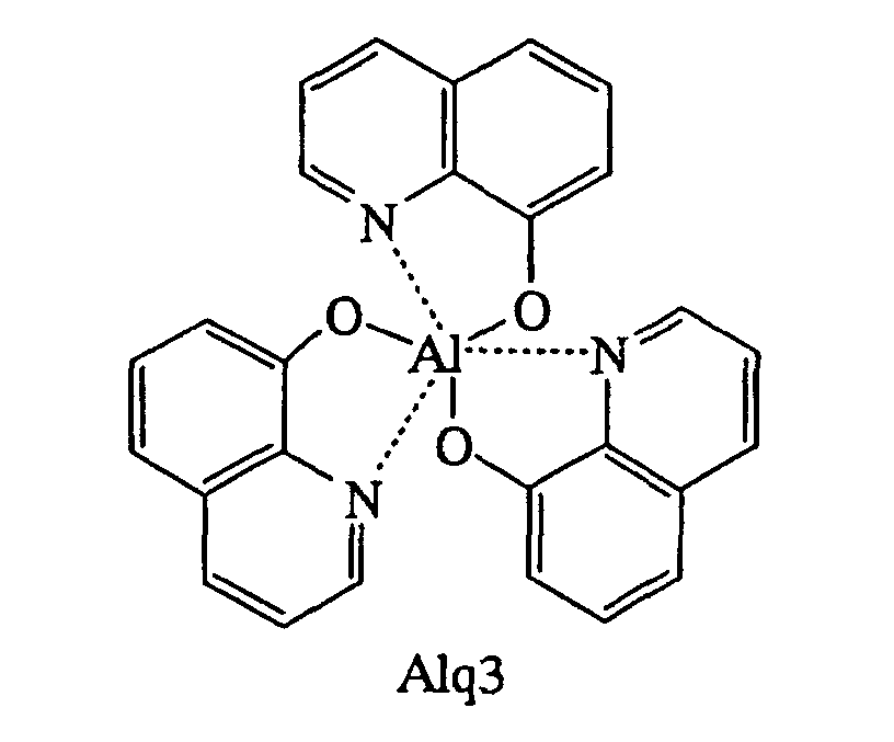
- the emission layer On the hole transport layer was formed the emission layer from commercial tris(8-hydroxyquinoline)aluminum (Alq3) (purified by sublimation).
- Alq3 commercial tris(8-hydroxyquinoline)aluminum
- the vacuum deposition of the emission layer was carried out at a degree of vacuum no higher than 8 ⁇ 10 -4 Pa.
- the vacuum deposition was also carried out at a rate of 0.3 nm/s until the deposited film became 50 nm thick.
- the electron injection layer was formed from lithium fluoride (LiF).
- the vacuum deposition of the electron injection layer was carried out at a degree of vacuum no higher than 8 ⁇ 10 -4 Pa.
- the vacuum deposition was also carried out at a rate of 0.01 nm/s until the deposited film became 0.5 nm thick.
- the cathode was formed from aluminum.
- the vacuum deposition of the cathode was carried out at a degree of vacuum no higher than 8 ⁇ 10 -4 Pa.
- the vacuum deposition was also carried out at a rate of 0.2 nm/s until the deposited film became 100 nm thick.
- Table 1 The characteristic properties shown in Table 1.
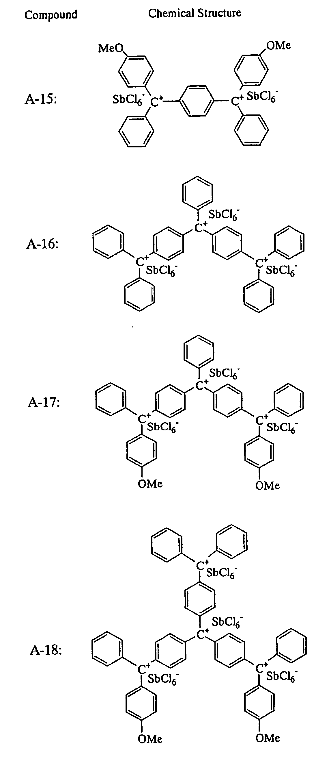
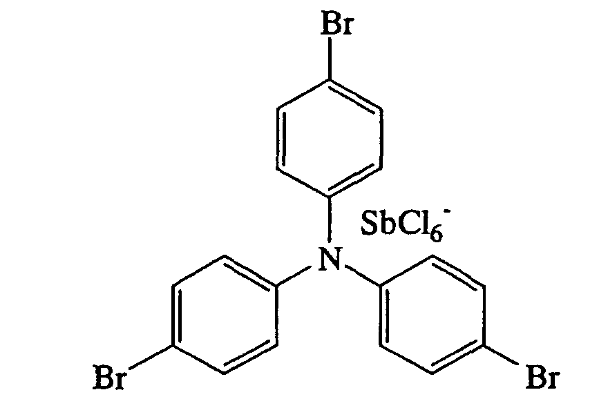
- the hole injection layer 3 was formed on the ITO substrate by spin coating under the following conditions from the compound designated as A-6 above.
- the hole injection layer 3 was formed from A-6 on the ITO glass substrate by spin coating under the following conditions.
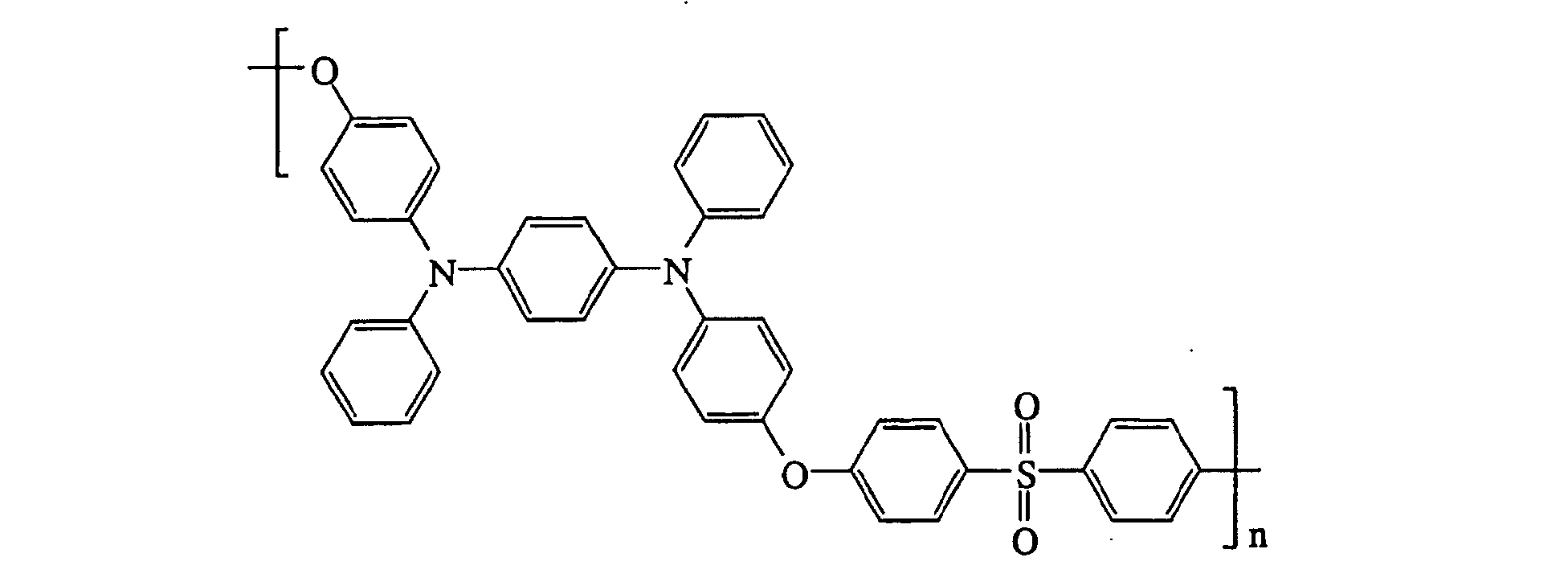
- the hole injection layer 3 was formed on the ITO glass substrate from a material composed of the triphenylamine-containing polyether (used in Comparative Example 2) and 30% by weight of A-6 (synthesized in Example 1), by spin coating under the same conditions as in Comparative Example 1.
- the triphenylamine-containing polyether was synthesized by the above-mentioned method proposed by Kido et al.
- the hole injection layer 3 was formed on the ITO glass substrate from a polyvinylcarbazole (reagent made by Kanto Kagaku) represented by the formula below, by spin coating under the same conditions as in Comparative Example 1.
- a polyvinylcarbazole (reagent made by Kanto Kagaku) represented by the formula below
- the hole injection layer 3 was formed on the ITO glass substrate from a material composed of the polyvinylcarbazole (used in Comparative Example 3) and 5% by weight of A-6, by spin coating under the same conditions as in Comparative Example 1.
- the hole injection layer 3 was formed on the ITO glass substrate from a material composed of the triphenylamine-containing polyether (used in Comparative Example 2) and 5% by weight of A-5, A-7, and A-8, respectively, by spin coating under the same conditions as in Comparative Example 1.
- Example 5 A-5, A-7, and A-8 were synthesized in the same way as in Example 1. Designation of compound Threshold voltage for emission (V) Voltage at 100 cd/m 2 (V) Voltage at 500 cd/m 2 (V) Comparative Example 1 6 10.5 11 Comparative Example 2 5 10 11.5 Comparative Example 3 10.5 16 17 Example 1 A-6 3.5 8 9.5 Example 3 A-6 3 6 8 Example 4 A-6 3 6.5 8.5 Example 5 A-6 3.5 11.5 13.5 Example 6 A-5 3 6 8 Example 7 A-7 3 6.5 9 Example 8 A-8 3 6.5 9
- the present invention makes it possible to easily produce long-lived defect-free organic electroluminescence devices capable of intensive emission at a low voltage.
- the organic electroluminescence device of the present invention is suitable for displays of various apparatus.
Landscapes
- Engineering & Computer Science (AREA)
- Chemical & Material Sciences (AREA)
- Materials Engineering (AREA)
- Physics & Mathematics (AREA)
- Spectroscopy & Molecular Physics (AREA)
- Manufacturing & Machinery (AREA)
- Organic Chemistry (AREA)
- Electroluminescent Light Sources (AREA)
Abstract
Description





These materials may be used alone or in combination with one another.



| Designation of compound | Threshold voltage for emission (V) | Voltage at 100 cd/m2 (V) | Voltage at 500 cd/m2 (V) | |
| Comparative Example 1 | 6 | 10.5 | 11 | |
| Comparative Example 2 | 5 | 10 | 11.5 | |
| Comparative Example 3 | 10.5 | 16 | 17 | |
| Example 1 | A-6 | 3.5 | 8 | 9.5 |
| Example 3 | | 3 | 6 | 8 |
| Example 4 | | 3 | 6.5 | 8.5 |
| Example 5 | A-6 | 3.5 | 11.5 | 13.5 |
| Example 6 | | 3 | 6 | 8 |
| Example 7 | | 3 | 6.5 | 9 |
| Example 8 | | 3 | 6.5 | 9 |
Claims (11)
- An organic electroluminescence device of the type having one or more than one emission layer in the form of thin film of an organic compound between paired electrodes, which includes at least one layer containing a compound with carbenium ions.
- The organic electroluminescence device as defined in Claim 1, wherein the compound with carbenium ions is one which is represented by the formula (1) below.(where Ar1 to Ar3 denote identical or different, substituted or unsubstituted aromatic groups, with at least one of them being a monovalent substituent group represented by the formula (2) below.
 where Ar4 to Ar6 denote substituted or unsubstituted aromatic groups which are identical with or different from Ar1 to Ar3, respectively; Y denotes a single bond, -O-, or a divalent organic group selected from C1-6 alkylene group, -COO-, -CONH-, 9H-fluorenylene group, and 9,9-dimethyl-9H-flurorenylene group; and R- denotes an anion species.)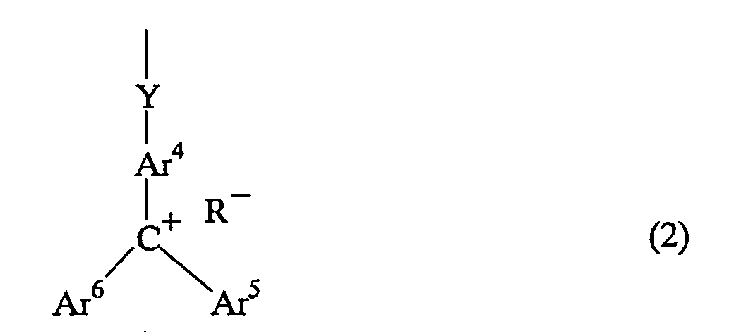
- The organic electroluminescence device as defined in Claim 1 or 2, wherein the layer containing the compound with carbenium ions is the hole transport layer.
- The organic electroluminescence device as defined in Claim 1 or 2, wherein the layer containing the compound with carbenium ions is the hole injection layer.
- The organic electroluminescence device as defined in Claim 1 or 2, wherein the layer containing the compound with carbenium ions is the electron transport layer.
- The organic electroluminescence device as defined in Claim 1 or 2, wherein the layer containing the compound with carbenium ions is the electron injection layer.
- A charge transport material which contains the compound with carbenium ions as defined in Claim 1 or 2.
- A hole transport material which contains the compound with carbenium ions as defined in Claim 1 or 2.
- A hole injection material which contains the compound with carbenium ions as defined in Claim 1 or 2.
- An electron transport material which contains the compound with carbenium ions as defined in Claim 1 or 2.
- An electron injection material which contains the compound with carbenium ions as defined in Claim 1 or 2.
Applications Claiming Priority (3)
| Application Number | Priority Date | Filing Date | Title |
|---|---|---|---|
| JP2002129608 | 2002-05-01 | ||
| JP2002129608 | 2002-05-01 | ||
| PCT/JP2003/005437 WO2003094578A1 (en) | 2002-05-01 | 2003-04-28 | Organic electroluminescence device and material thereof |
Publications (3)
| Publication Number | Publication Date |
|---|---|
| EP1501337A1 true EP1501337A1 (en) | 2005-01-26 |
| EP1501337A4 EP1501337A4 (en) | 2009-05-06 |
| EP1501337B1 EP1501337B1 (en) | 2012-12-12 |
Family
ID=29397308
Family Applications (1)
| Application Number | Title | Priority Date | Filing Date |
|---|---|---|---|
| EP03725696A Expired - Lifetime EP1501337B1 (en) | 2002-05-01 | 2003-04-28 | Organic electroluminescence device and material thereof |
Country Status (8)
| Country | Link |
|---|---|
| US (1) | US7358660B2 (en) |
| EP (1) | EP1501337B1 (en) |
| JP (1) | JP4381298B2 (en) |
| KR (1) | KR100954779B1 (en) |
| CN (1) | CN100479223C (en) |
| AU (1) | AU2003231549A1 (en) |
| TW (1) | TWI281491B (en) |
| WO (1) | WO2003094578A1 (en) |
Cited By (2)
| Publication number | Priority date | Publication date | Assignee | Title |
|---|---|---|---|---|
| EP2485290A4 (en) * | 2009-10-01 | 2013-03-06 | Hitachi Chemical Co Ltd | ORGANIC ELECTRONIC MATERIAL, ORGANIC ELECTRONIC ELEMENT, ORGANIC ELECTROLUMINESCENT ELEMENT, DISPLAY ELEMENT USING ORGANIC ELECTROLUMINESCENT ELEMENT, ILLUMINATING DEVICE, AND DISPLAY DEVICE |
| EP2562839A4 (en) * | 2010-04-22 | 2015-07-22 | Hitachi Chemical Co Ltd | Organic electronic material, polymerization initiator and thermal polymerization initiator, ink composition, organic thin film and production method for same, organic electronic element, organic electroluminescent element, lighting device, display element, and display device |
Families Citing this family (5)
| Publication number | Priority date | Publication date | Assignee | Title |
|---|---|---|---|---|
| TW200517469A (en) * | 2003-10-30 | 2005-06-01 | Nissan Chemical Ind Ltd | Charge-transporting compound, charge-transporting material, charge-transporting varnish, charge-transporting thin film, and organic electroluminescent device |
| KR100669757B1 (en) * | 2004-11-12 | 2007-01-16 | 삼성에스디아이 주식회사 | Organic electroluminescent element |
| KR100858824B1 (en) | 2007-05-31 | 2008-09-17 | 삼성에스디아이 주식회사 | Organic light emitting device and method for manufacturing same |
| US8476822B2 (en) * | 2007-11-09 | 2013-07-02 | Universal Display Corporation | Saturated color organic light emitting devices |
| CN104333932B (en) * | 2014-03-26 | 2017-01-18 | 南京第壹有机光电有限公司 | Adjustable organic electroluminescence illuminating lamp |
Family Cites Families (35)
| Publication number | Priority date | Publication date | Assignee | Title |
|---|---|---|---|---|
| DE2425193A1 (en) * | 1974-05-24 | 1975-12-04 | Bayer Ag | METHOD FOR MANUFACTURING ALPHA. ALPHA.ALPHA.ALPHA'.ALPHA'.ALPHA'-HEXAKISARYL-1.3- OR 1.4-DIMETHYLBENZENE |
| DE2425194A1 (en) * | 1974-05-24 | 1975-12-11 | Bayer Ag | Tetrakis-aryl-di-chloro- and -di-hydroxy-xylenes prodn - from meta- or para-hexachloroxylene and aromatic cpd. by Friedel Crafts reaction |
| US4764625A (en) | 1980-12-12 | 1988-08-16 | Xerox Corporation | Process for preparing arylamines |
| US4379070A (en) * | 1982-04-26 | 1983-04-05 | Corning Glass Works | Tin-phosphorus oxyfluoride glass containing aromatic organic compound |
| US4539507A (en) | 1983-03-25 | 1985-09-03 | Eastman Kodak Company | Organic electroluminescent devices having improved power conversion efficiencies |
| US4720432A (en) | 1987-02-11 | 1988-01-19 | Eastman Kodak Company | Electroluminescent device with organic luminescent medium |
| JP2670121B2 (en) | 1988-12-14 | 1997-10-29 | 出光興産株式会社 | Organic thin-film electroluminescence device |
| EP0349034B1 (en) | 1988-06-28 | 1994-01-12 | Agfa-Gevaert N.V. | Electrophotographic recording material |
| JPH03296595A (en) | 1990-04-13 | 1991-12-27 | Kao Corp | Organic thin film electroluminescent element |
| JPH04175395A (en) | 1990-07-06 | 1992-06-23 | Ricoh Co Ltd | Electroluminescent |
| US5061569A (en) | 1990-07-26 | 1991-10-29 | Eastman Kodak Company | Electroluminescent device with organic electroluminescent medium |
| JP3150330B2 (en) | 1990-09-19 | 2001-03-26 | 株式会社東芝 | Organic thin film element |
| JPH04264189A (en) | 1991-02-18 | 1992-09-18 | Fuji Electric Co Ltd | Electroluminescent element |
| US5330866A (en) | 1991-02-18 | 1994-07-19 | Minolta Camera Kabushiki Kaisha | Photosensitive member comprising an amino compound |
| JP3185280B2 (en) | 1991-02-18 | 2001-07-09 | ミノルタ株式会社 | Novel benzyldiphenyl compound, photoreceptor and electroluminescent device using the benzyldiphenyl compound |
| JPH04304466A (en) | 1991-04-02 | 1992-10-27 | Fuji Electric Co Ltd | Organic thin-film light emitting element |
| JP3016896B2 (en) | 1991-04-08 | 2000-03-06 | パイオニア株式会社 | Organic electroluminescence device |
| JP3065130B2 (en) | 1991-07-22 | 2000-07-12 | 三井化学株式会社 | Organic electroluminescent device |
| US5274058A (en) * | 1991-09-12 | 1993-12-28 | Board Of Regents, The University Of Texas System | Low bandgap polymers rf fused bithiophenes |
| JP3565870B2 (en) | 1992-02-25 | 2004-09-15 | 株式会社リコー | Electroluminescent device |
| JPH05310949A (en) | 1992-05-08 | 1993-11-22 | Toppan Printing Co Ltd | Polyphosphazene compound |
| JP3463358B2 (en) | 1994-07-08 | 2003-11-05 | 東洋インキ製造株式会社 | Hole transport material and its use |
| JP3593719B2 (en) | 1994-08-04 | 2004-11-24 | 東洋インキ製造株式会社 | Novel triphenylamine derivative, its production method and use |
| JP3593717B2 (en) | 1994-08-04 | 2004-11-24 | 東洋インキ製造株式会社 | Novel triphenylamine derivative, its production method and use |
| JP3643452B2 (en) | 1995-11-10 | 2005-04-27 | ケミプロ化成株式会社 | Aromatic diamine-containing polyether and organic EL device using the same |
| JP3748491B2 (en) | 1998-03-27 | 2006-02-22 | 出光興産株式会社 | Organic electroluminescence device |
| JP4058842B2 (en) | 1998-05-13 | 2008-03-12 | 三菱化学株式会社 | Organic electroluminescence device |
| JP2000091077A (en) * | 1998-09-11 | 2000-03-31 | Sony Corp | Organic electroluminescent device |
| JP4824848B2 (en) | 2000-02-29 | 2011-11-30 | 淳二 城戸 | Organic electroluminescent device, organic electroluminescent device group, and method for identifying emission spectrum thereof |
| KR20010050711A (en) | 1999-09-29 | 2001-06-15 | 준지 키도 | Organic electroluminescent device, group of organic electroluminescent devices and controlling method of emission spectrum in such devices |
| GB0007530D0 (en) * | 2000-03-28 | 2000-05-17 | Isis Innovation | Trityl-type compounds and their use |
| JP4144192B2 (en) | 2000-05-29 | 2008-09-03 | 三菱化学株式会社 | Method for manufacturing organic electroluminescent device |
| JP2003068464A (en) | 2001-08-27 | 2003-03-07 | Canon Inc | Organic light emitting device |
| WO2004099340A1 (en) * | 2003-05-12 | 2004-11-18 | Sumitomo Chemical Company, Limited | Luminescent-polymer composition |
| DE602004021393D1 (en) * | 2004-04-27 | 2009-07-16 | Xsys Print Solutions Us Llc | LOADING AGENT WITH A MIXTURE OF TRIPHENYLMETHANE COMPOUND AND TETRAPHENYLMETHANE |
-
2003
- 2003-04-28 KR KR1020047017530A patent/KR100954779B1/en not_active Expired - Fee Related
- 2003-04-28 US US10/512,988 patent/US7358660B2/en not_active Expired - Fee Related
- 2003-04-28 WO PCT/JP2003/005437 patent/WO2003094578A1/en not_active Ceased
- 2003-04-28 EP EP03725696A patent/EP1501337B1/en not_active Expired - Lifetime
- 2003-04-28 AU AU2003231549A patent/AU2003231549A1/en not_active Abandoned
- 2003-04-28 CN CNB038118238A patent/CN100479223C/en not_active Expired - Fee Related
- 2003-04-28 JP JP2004502680A patent/JP4381298B2/en not_active Expired - Fee Related
- 2003-04-30 TW TW092110190A patent/TWI281491B/en active
Cited By (4)
| Publication number | Priority date | Publication date | Assignee | Title |
|---|---|---|---|---|
| EP2485290A4 (en) * | 2009-10-01 | 2013-03-06 | Hitachi Chemical Co Ltd | ORGANIC ELECTRONIC MATERIAL, ORGANIC ELECTRONIC ELEMENT, ORGANIC ELECTROLUMINESCENT ELEMENT, DISPLAY ELEMENT USING ORGANIC ELECTROLUMINESCENT ELEMENT, ILLUMINATING DEVICE, AND DISPLAY DEVICE |
| US9583714B2 (en) | 2009-10-01 | 2017-02-28 | Hitachi Chemical Company, Ltd. | Material for organic electronics, organic electronic element, organic electroluminescent element, display element using organic electroluminescent element, illuminating device, and display device |
| EP2562839A4 (en) * | 2010-04-22 | 2015-07-22 | Hitachi Chemical Co Ltd | Organic electronic material, polymerization initiator and thermal polymerization initiator, ink composition, organic thin film and production method for same, organic electronic element, organic electroluminescent element, lighting device, display element, and display device |
| US10566105B2 (en) | 2010-04-22 | 2020-02-18 | Hitachi Chemical Company, Ltd. | Method for producing charge transport film |
Also Published As
| Publication number | Publication date |
|---|---|
| US20050221117A1 (en) | 2005-10-06 |
| TWI281491B (en) | 2007-05-21 |
| WO2003094578A1 (en) | 2003-11-13 |
| TW200307736A (en) | 2003-12-16 |
| KR100954779B1 (en) | 2010-04-28 |
| EP1501337A4 (en) | 2009-05-06 |
| JP4381298B2 (en) | 2009-12-09 |
| EP1501337B1 (en) | 2012-12-12 |
| AU2003231549A1 (en) | 2003-11-17 |
| CN1656855A (en) | 2005-08-17 |
| JPWO2003094578A1 (en) | 2005-09-08 |
| KR20050007358A (en) | 2005-01-17 |
| US7358660B2 (en) | 2008-04-15 |
| CN100479223C (en) | 2009-04-15 |
Similar Documents
| Publication | Publication Date | Title |
|---|---|---|
| US5948552A (en) | Heat-resistant organic electroluminescent device | |
| US7737248B2 (en) | Charge-transporting compound, charge-transporting material, charge-transporting varnish, charge-transporting thin film, and organic electroluminescent device | |
| JP5193074B2 (en) | Organic EL device | |
| KR100825211B1 (en) | Cyclic tertiary amine compound and organic electroluminescent device containing the same | |
| JP4722695B2 (en) | Organic light emitting device | |
| EP0866110A1 (en) | Light-emitting material for organo-electroluminescence device and organic electroluminescence device | |
| KR20020062932A (en) | Novel styryl compounds and organic electroluminescent devices | |
| JP4258583B2 (en) | Electroluminescent device | |
| US7358660B2 (en) | Organic electroluminescence device and material thereof | |
| JP4314771B2 (en) | Organic electroluminescence device | |
| JP4069505B2 (en) | Trinaphthylbenzene derivative and organic electroluminescence device using the same | |
| JP2003007470A (en) | Organic electric field emitting element | |
| JP4375502B2 (en) | Light emitting element | |
| KR20030012933A (en) | Charge-transporting material containing diazapentacene derivative, luminescent material, and organic electroluminescent element employing these | |
| JP2004087372A (en) | Organic electroluminescent device | |
| JPH08283416A (en) | Cyclic phosphazene compound and organic thin film el element | |
| JP4109292B2 (en) | Compounds for organic EL devices | |
| JP2009064968A (en) | Organic electroluminescent element and display unit |
Legal Events
| Date | Code | Title | Description |
|---|---|---|---|
| PUAI | Public reference made under article 153(3) epc to a published international application that has entered the european phase |
Free format text: ORIGINAL CODE: 0009012 |
|
| 17P | Request for examination filed |
Effective date: 20041116 |
|
| AK | Designated contracting states |
Kind code of ref document: A1 Designated state(s): AT BE BG CH CY CZ DE DK EE ES FI FR GB GR HU IE IT LI LU MC NL PT RO SE SI SK TR |
|
| AX | Request for extension of the european patent |
Extension state: AL LT LV MK |
|
| A4 | Supplementary search report drawn up and despatched |
Effective date: 20090402 |
|
| 17Q | First examination report despatched |
Effective date: 20091008 |
|
| REG | Reference to a national code |
Ref country code: DE Ref legal event code: R079 Ref document number: 60342839 Country of ref document: DE Free format text: PREVIOUS MAIN CLASS: H05B0033220000 Ipc: H01L0051500000 |
|
| GRAP | Despatch of communication of intention to grant a patent |
Free format text: ORIGINAL CODE: EPIDOSNIGR1 |
|
| RIC1 | Information provided on ipc code assigned before grant |
Ipc: H01L 51/50 20060101AFI20120614BHEP |
|
| RIN1 | Information on inventor provided before grant (corrected) |
Inventor name: YOSHIMOTO,TAKUJI C/O ELECTRONIC MATERIALS RESEARCH Inventor name: YAMADA,TOMOHISA, C/O ELECTRONIC MATERIALS RESEARCH |
|
| GRAS | Grant fee paid |
Free format text: ORIGINAL CODE: EPIDOSNIGR3 |
|
| GRAA | (expected) grant |
Free format text: ORIGINAL CODE: 0009210 |
|
| RBV | Designated contracting states (corrected) |
Designated state(s): DE FR GB |
|
| AK | Designated contracting states |
Kind code of ref document: B1 Designated state(s): DE FR GB |
|
| REG | Reference to a national code |
Ref country code: GB Ref legal event code: FG4D |
|
| REG | Reference to a national code |
Ref country code: DE Ref legal event code: R096 Ref document number: 60342839 Country of ref document: DE Effective date: 20130207 |
|
| PGFP | Annual fee paid to national office [announced via postgrant information from national office to epo] |
Ref country code: GB Payment date: 20130320 Year of fee payment: 11 |
|
| PGFP | Annual fee paid to national office [announced via postgrant information from national office to epo] |
Ref country code: DE Payment date: 20130321 Year of fee payment: 11 |
|
| PGFP | Annual fee paid to national office [announced via postgrant information from national office to epo] |
Ref country code: FR Payment date: 20130417 Year of fee payment: 11 |
|
| PLBE | No opposition filed within time limit |
Free format text: ORIGINAL CODE: 0009261 |
|
| STAA | Information on the status of an ep patent application or granted ep patent |
Free format text: STATUS: NO OPPOSITION FILED WITHIN TIME LIMIT |
|
| 26N | No opposition filed |
Effective date: 20130913 |
|
| REG | Reference to a national code |
Ref country code: DE Ref legal event code: R097 Ref document number: 60342839 Country of ref document: DE Effective date: 20130913 |
|
| REG | Reference to a national code |
Ref country code: DE Ref legal event code: R119 Ref document number: 60342839 Country of ref document: DE |
|
| GBPC | Gb: european patent ceased through non-payment of renewal fee |
Effective date: 20140428 |
|
| REG | Reference to a national code |
Ref country code: DE Ref legal event code: R119 Ref document number: 60342839 Country of ref document: DE Effective date: 20141101 |
|
| REG | Reference to a national code |
Ref country code: FR Ref legal event code: ST Effective date: 20141231 |
|
| PG25 | Lapsed in a contracting state [announced via postgrant information from national office to epo] |
Ref country code: GB Free format text: LAPSE BECAUSE OF NON-PAYMENT OF DUE FEES Effective date: 20140428 Ref country code: DE Free format text: LAPSE BECAUSE OF NON-PAYMENT OF DUE FEES Effective date: 20141101 |
|
| PG25 | Lapsed in a contracting state [announced via postgrant information from national office to epo] |
Ref country code: FR Free format text: LAPSE BECAUSE OF NON-PAYMENT OF DUE FEES Effective date: 20140430 |