EP1501195A1 - Anordnung zur Generierung eines Taktsignals für einen Sigma-Delta-Analog-Digital-Wandler - Google Patents
Anordnung zur Generierung eines Taktsignals für einen Sigma-Delta-Analog-Digital-Wandler Download PDFInfo
- Publication number
- EP1501195A1 EP1501195A1 EP03016974A EP03016974A EP1501195A1 EP 1501195 A1 EP1501195 A1 EP 1501195A1 EP 03016974 A EP03016974 A EP 03016974A EP 03016974 A EP03016974 A EP 03016974A EP 1501195 A1 EP1501195 A1 EP 1501195A1
- Authority
- EP
- European Patent Office
- Prior art keywords
- clock signal
- analog
- frequency
- signal
- digital converter
- Prior art date
- Legal status (The legal status is an assumption and is not a legal conclusion. Google has not performed a legal analysis and makes no representation as to the accuracy of the status listed.)
- Granted
Links
Images


Classifications
-
- G—PHYSICS
- G01—MEASURING; TESTING
- G01R—MEASURING ELECTRIC VARIABLES; MEASURING MAGNETIC VARIABLES
- G01R31/00—Arrangements for testing electric properties; Arrangements for locating electric faults; Arrangements for electrical testing characterised by what is being tested not provided for elsewhere
- G01R31/28—Testing of electronic circuits, e.g. by signal tracer
- G01R31/3167—Testing of combined analog and digital circuits
-
- G—PHYSICS
- G06—COMPUTING OR CALCULATING; COUNTING
- G06F—ELECTRIC DIGITAL DATA PROCESSING
- G06F3/00—Input arrangements for transferring data to be processed into a form capable of being handled by the computer; Output arrangements for transferring data from processing unit to output unit, e.g. interface arrangements
- G06F3/05—Digital input using the sampling of an analogue quantity at regular intervals of time, input from a/d converter or output to d/a converter
Definitions
- the invention relates to a method and a device according to the The preambles of claims 1 and 3.
- Such methods and arrangements are useful in translating analog Signals into digital signals, for example in a monitoring device, Control and regulation of a technical installation of a building.
- the operational system is an example of a heating, ventilation and Air conditioning, with access and fire control equipment or generally one Building automation system or a building management system.
- indoor climate systems such as Room temperature, humidity and air quality are affected.
- field devices such as sensors and Serve actuators by electrical signals.
- analog Signals of the field devices for transmission and / or processing by analog-to-digital converters converted into digital signals.
- an analog signal is unfortunately also superimposed by a disturbance variable, which by electrical and / or magnetic fields of the power grid or by connected to the power grid components on the analogue useful signal can be modulated.
- the analogue useful signal is for example the a measured physical quantity corresponding signal of a sensor; for example, a temperature or humidity sensor.
- the said disturbance has the frequency of the power supply network and is also called network hum designated. Especially with analog signals in a building is the mains hum often not negligible.
- the sigma-delta method when sampling an analog signal and the decimation rate
- the sigma-delta method can also be used as a filter for certain frequencies of the analog signal act.
- the mains hum can only be achieved if the sample rate and the Frequency of the power supply network formed quotient is constant.
- the sample rate is derived from a quartz stabilized oscillator.
- the frequency of the power grid is in certain regions and countries 50 Hz in others, however, 60 Hz.
- the frequency can vary depending on the quality of the power supply network deviate from a nominal value. In the present case is calculated with a rejection of +/- 4% of the nominal value.
- the invention is based on the object, a method for generating a Sample clock signal for a sigma-delta method analog-to-digital converter indicate which in all regions the mains hum enough suppressed.
- a facility is to be created with which the Method is feasible.
- Fig. 1 denotes a clock generator comprising an oscillator 2, a Counter 3 and an accumulator 4 has.
- the oscillator 2 generates a System clock signal C, the counter 3 and the accumulator 4 and with Advantage is also performed on a first connection point 5 of the clock generator 1.
- the oscillator 2 is preferably stabilized via an externally arranged quartz, the example of a second connection point XTAL and a third Connection point EXTAL of the clock generator 1 with the oscillator 2 is connectable.
- the accumulator unit 4 advantageously has an adder register 10, another one Register 11 and an output 12 for an output signal 13.
- the clock generator 1 advantageously also has a signal converter 15, through the one lying on an input of the signal converter 15 sinusoidal AC voltage Us is converted into a rectangular signal Ur, that of an output of the signal converter 15 is guided to an input 16 of the counter 3 and which has the period T of the AC voltage Us.
- a signal converter 15 is an example of a comparator circuit.
- the AC voltage Us is taken from the power supply network PL and advantageously before the supply via a fourth connection point 16 in one Adjustment member 17 suppressed and brought to a required voltage level.
- the frequency of AC voltage supplied by the power supply network PL depending By region typically 50 Hz or 60 Hz, and also the Nominal frequency can fluctuate within certain tolerance limits, here is the frequency of the power supply network PL and of course the associated Period T generally variable.
- the adaptation element 17 advantageously comprises a low-pass filter.
- the Adaptation member 17 is typically not together with the clock generator 1 in FIG integrated into a module.
- the stated object is achieved by a method in which a first method step, the variable period T of Power supply network PL is determined in units of time of the system clock signal C and further in a second method step, a sampling clock signal S by distributing a constant number K pulses is generated over the determined period T, so that the frequency of the sampling clock signal S is an integer multiple of the Frequency of the power grid is.
- the sampling clock signal S for sampling a supplied Analog signal Ua is used, the mains hum of the analog signal Ua at the Sampling optimally suppressed or filtered out. That of the analog-to-digital converter 20 generated from the analog signal Ua digital signal Ud is thus also then optimally freed from mains hum when the frequency of the Power supply network PL changes.
- the automatic optimal suppression of the Network hum is achieved regardless of whether the clock generator 1 in Regions with different frequency of the power supply network PL used or whether the frequency of the power supply PL for other reasons fluctuates.
- the system clock signal C is also for Other clocks, not in the context of the present invention addressed components - such as microprocessors or Multiplexer - can be used, whose requirements are the required frequency of the System clock signal C can determine.
- the frequency of the system clock signal C about 5 MHz.
- the period T of the power supply network PL in Time units of the system clock signal C.
- Ur determined pulses of the system clock signal C determined Period T is available at an output 22 of the counter 3.
- the determined period T in the register 11th stored and count limit or maximum value for the adder register 10th used.
- the current content A of the Add register 10 by a constant value W increases, with a Exceeding the count limit at the output 12, a pulse of the output signal 13th is generated, and in the adder register 10 only a residual value is stored.
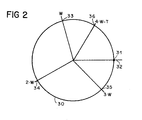
- the principle of operation of the accumulator unit is shown in FIG. 2 illustrated.
- the current period T is defined by the circumference of a circle 30 shown.
- An intersection 31 of the circle 30 with a center line 32 represents both the minimum content A of the adder register 10 - namely zero - as well as the maximum Content A - namely the count limit - with each pulse of the system clock signal C is added to the current content A the constant value W. If you start at zero, Thus, the adder register 10 in the example shown after the first pulse the with a point 33 shown value W, after the second pulse with a Point 34 shown double value W and after the third pulse with a Point 35, three times the value W.
- the Intersection 31 exceeded the count limit, at the output 12 of the Accumulator 4 (Fig. 1) generates a pulse of the output signal 13 and the Content A of the adder register 10 to the one represented by a point 36 Period T decreased to four times the value W is set.
- this model changes the circumference of the circle 30 according to a possible change in the Frequency of the power supply network.
- the frequency of the power supply network is 50 Hz and the frequency of the system clock signal is 5 MHz.
- the constant value W is 16'384, that is 2 14 .
- the circumference of circle 30 thus corresponds to a number 100,000.
- the content A of the adder register 10 is shown in the following table for eight pulses of the system clock signal C starting from zero: Pulse of the system clock signal Content A Pulse at the output 12 0 0 No 1 16384 No 2 32768 No 3 49152 No 4 65536 No 5 81920 No 6 98304 No 7 14688 Yes 8th 31072 No
- the am Output 12 of the accumulator 4 Whenever the counting limit is exceeded in the adder register 10, the am Output 12 of the accumulator 4 generates a pulse. This will be in the example 16'384 pulses evenly over the measured period T of Distributed power supply network.
- determining the period T errors may occur, for example by disturbances of the applied at the fourth connection point 16 sinusoidal AC voltage Us are caused, and exemplified by a low-pass filter are correctable.
- a digital filter 40 between the counter 3 and the accumulator unit 4 is switched.
- the counted by the counter 3 period T is implemented by the digital filter 40 in a filtered period T *.
- the im Register 11 stored count limit is thus 40 when using the filter filtered period T *.
- the sampling clock signal S available at a fifth connection point 41 is stored in Clock generator 1 processed so that the network hum of the analog-to-digital converter 20 sampled analog signal Ua is optimally suppressed in the sampling.
- the Desired optimum rejection is achieved when the rate of the sample clock signal S equal to that from the frequency of the power supply network and the Decimation rate of the applied analog-to-digital converter 20 is formed product.
- a sampling clock signal S which has per pulse of the power supply constantly 8192 pulses, which are divided evenly over a period of the power grid.
- the sigma-delta method analog-to-digital converter 20 requires typically a symmetric sample clock signal S, ie pulse and pause should be the same length.
- the sampling clock signal S is sufficiently symmetrically generated when it is at the output an advantageously by the system clock signal C clocked frequency divider stage 42nd whose input is connected to the output signal 13 of the accumulator 4 is fed. A made by the frequency divider stage 42 lowering the Frequency is in the accumulator 4 by a corresponding increase of the constant value W.
- the frequency divider stage 42 halves the frequency of the by the Accumulator 4 supplied output signal 13, which in the accumulator unit. 4 is compensated when the constant value W is at twice the decimation rate of the Analog-to-digital converter 20 is set.
- the constant value W on the decimation rate of the analog-to-digital converter 20 set.
- a constant ratio between the rate of the sample clock signal S and the Frequency of the power supply network PL could also be a so-called Achieve phase-locked loop (PLL).
- PLL phase-locked loop
- ASIC application-specific Implement Integrated Circuit
- the ASIC 50 includes the clock generator 1, the analog-to-digital converter 20 and also at least one multiplexer 51 and a communication interface 52.
- About the Multiplexer 51 is the analog-to-digital converter 20 on the input side terminals 55, 56, 57th or 58 switchable, which in turn are connectable to different field devices.
- the applied analogue signal Ua is generated by the clock generator 1 Sample clock signal S read.
- About another terminal 59 is the clock generator 1 with an AC voltage of the power supply network connectable.
- On the output side is the analog-to-digital converter 20 via the communication interface 52 with example connectable to a processor connected to a port 60.
Landscapes
- Engineering & Computer Science (AREA)
- Physics & Mathematics (AREA)
- General Engineering & Computer Science (AREA)
- General Physics & Mathematics (AREA)
- Theoretical Computer Science (AREA)
- Human Computer Interaction (AREA)
- Compression, Expansion, Code Conversion, And Decoders (AREA)
Abstract
Description
- Fig. 1
- ein Blockschaltbild mit einem Analog-Digital-Wandler und einer Anordnung zur Generierung eines Abtasttakt-Signals,
- Fig. 2
- eine Darstellung zur Funktionsweise der Anordnung, und
- Fig. 3
- ein Blockschaltbild zur Anwendung der Anordnung.
| Impuls des Systemtakt-Signals | Inhalt A | Impuls am Ausgang 12 |
| 0 | 0 | nein |
| 1 | 16384 | nein |
| 2 | 32768 | nein |
| 3 | 49152 | nein |
| 4 | 65536 | nein |
| 5 | 81920 | nein |
| 6 | 98304 | nein |
| 7 | 14688 | ja |
| 8 | 31072 | nein |
Claims (7)
- Verfahren zur Generierung eines Abtasttakt-Signals (S) zur Abtastung eines Analogsignals (Ua) für einen nach dem Sigma-Delta-Verfahren arbeitenden Analog-Digital-Wandler (20), mit den Verfahrensschritten:Ermitteln einer variablen Periodendauer (T; T*) des Energieversorgungsnetzes (PL) in Zeiteinheiten eines Systemtakt-Signals (C), undGenerieren des Abtasttakt-Signals (S) durch Verteilen einer konstanten Anzahl K Impulse über die ermittelte Periodendauer (T; T*), sodass die Frequenz des Abtasttakt-Signals (S) ein ganzzahliges Vielfaches der Frequenz des Energieversorgungsnetzes (PL) ist.
- Verfahren nach Anspruch 1, dadurch gekennzeichnet, dass die Anzahl K gleich dem Wert der Dezimationsrate des Analog-Digital-Wandlers (20) ist.
- Einrichtung zur Durchführung eines Verfahrens nach einem der Ansprüche 1 oder 2, gekennzeichnet durcheinen mit dem Systemtakt-Signal (C) taktbaren Zähler (3), wobei an einem Eingang (16) des Zählers (3) ein vom Energieversorgungsnetz (PL) abgeleitetes Signal (Ur) leitbar ist, so dass die Periodendauer (T) des Energieversorgungsnetzes (PL) in Zeiteinheiten des Systemtakt-Signals (C) durch den Zähler (3) zählbar ist,eine mit dem Systemtakt-Signal (C) taktbare ein Addierregister (10) aufweisende Akkumulatoreinheit (4), der die gezählte Periodendauer (T; T*) als Zählgrenze zuweisbar ist und in der der aktuelle Wert (A) des Addierregisters (10) mit jedem Impuls des Systemtakt-Signals (C) um einen konstanten Wert W erhöhbar ist, wobei die Akkumulatoreinheit (4) einen Ausgang (12) für das Abtasttaktsignal (13) aufweist, an dem bei einem Überschreiten der Zählgrenze ein Impuls generierbar ist.
- Einrichtung nach Anspruch 3, gekennzeichnet durch ein zwischen den Zähler (3) und die Akkumulatoreinheit (4) geschaltetes digitales Filter (40), durch welches die vom Zähler (3) gezählte Periodendauer (T) filterbar ist.
- Einrichtung nach einem der Ansprüche 3 oder 4, dadurch gekennzeichnet, dass der Wert W gleich dem Wert der Dezimationsrate des Analog-Digital-Wandlers (20) ist.
- Einrichtung nach einem der Ansprüche 3 oder 4, dadurch gekennzeichnet, dass der Wert W gleich dem doppelten Wert der Dezimationsrate des Analog-Digital-Wandlers (20) ist.
- Einrichtung nach Anspruch 6, gekennzeichnet durch einen der Akkumulatoreinheit (4) nachgeschalteten Frequenzteiler (42), durch den die Frequenz des Ausgangssignals (13) der Akkumulatoreinheit (4) halbierbar ist.
Priority Applications (3)
| Application Number | Priority Date | Filing Date | Title |
|---|---|---|---|
| DE50303038T DE50303038D1 (de) | 2003-07-25 | 2003-07-25 | Anordnung zur Generierung eines Taktsignals für einen Sigma-Delta-Analog-Digital-Wandler |
| EP03016974A EP1501195B1 (de) | 2003-07-25 | 2003-07-25 | Anordnung zur Generierung eines Taktsignals für einen Sigma-Delta-Analog-Digital-Wandler |
| AT03016974T ATE323971T1 (de) | 2003-07-25 | 2003-07-25 | Anordnung zur generierung eines taktsignals für einen sigma-delta-analog-digital-wandler |
Applications Claiming Priority (1)
| Application Number | Priority Date | Filing Date | Title |
|---|---|---|---|
| EP03016974A EP1501195B1 (de) | 2003-07-25 | 2003-07-25 | Anordnung zur Generierung eines Taktsignals für einen Sigma-Delta-Analog-Digital-Wandler |
Publications (2)
| Publication Number | Publication Date |
|---|---|
| EP1501195A1 true EP1501195A1 (de) | 2005-01-26 |
| EP1501195B1 EP1501195B1 (de) | 2006-04-19 |
Family
ID=33483947
Family Applications (1)
| Application Number | Title | Priority Date | Filing Date |
|---|---|---|---|
| EP03016974A Expired - Lifetime EP1501195B1 (de) | 2003-07-25 | 2003-07-25 | Anordnung zur Generierung eines Taktsignals für einen Sigma-Delta-Analog-Digital-Wandler |
Country Status (3)
| Country | Link |
|---|---|
| EP (1) | EP1501195B1 (de) |
| AT (1) | ATE323971T1 (de) |
| DE (1) | DE50303038D1 (de) |
Citations (3)
| Publication number | Priority date | Publication date | Assignee | Title |
|---|---|---|---|---|
| US4993052A (en) * | 1988-08-01 | 1991-02-12 | Diehl Gmbh & Co. | Digitally-operating electrical equipment with counter for automatically adapting output to 50 Hz or 60 Hz input |
| US5349352A (en) * | 1992-12-21 | 1994-09-20 | Harris Corporation | Analog-to-digital converter having high AC line noise rejection and insensitive to AC line frequency variations |
| JP2002196024A (ja) * | 2000-12-26 | 2002-07-10 | Mitsubishi Electric Corp | 周期計測回路 |
-
2003
- 2003-07-25 EP EP03016974A patent/EP1501195B1/de not_active Expired - Lifetime
- 2003-07-25 DE DE50303038T patent/DE50303038D1/de not_active Expired - Lifetime
- 2003-07-25 AT AT03016974T patent/ATE323971T1/de active
Patent Citations (3)
| Publication number | Priority date | Publication date | Assignee | Title |
|---|---|---|---|---|
| US4993052A (en) * | 1988-08-01 | 1991-02-12 | Diehl Gmbh & Co. | Digitally-operating electrical equipment with counter for automatically adapting output to 50 Hz or 60 Hz input |
| US5349352A (en) * | 1992-12-21 | 1994-09-20 | Harris Corporation | Analog-to-digital converter having high AC line noise rejection and insensitive to AC line frequency variations |
| JP2002196024A (ja) * | 2000-12-26 | 2002-07-10 | Mitsubishi Electric Corp | 周期計測回路 |
Also Published As
| Publication number | Publication date |
|---|---|
| ATE323971T1 (de) | 2006-05-15 |
| EP1501195B1 (de) | 2006-04-19 |
| DE50303038D1 (de) | 2006-05-24 |
Similar Documents
| Publication | Publication Date | Title |
|---|---|---|
| DE102016119419B4 (de) | Universelle Sensorschnittstelle eines Maschinenüberwachungssystems | |
| EP0401562A2 (de) | Anordnung zur Umsetzung eines Signals mit einer ersten Abtastrate in ein Signal mit einer zweiten Abtastrate | |
| DE69123388T2 (de) | Analog-Digitalumsetzer | |
| DE69410913T2 (de) | Synchronisierungsschaltung mit einem schnellen digitalen Schlupffrequenzzähler | |
| WO2005085881A1 (de) | Energiezähleranordnung und verfahren zum kalibrieren | |
| EP0321725B1 (de) | Verfahren zum Ermitteln einer Ansteuerspannung eines spannungsgesteuerten Oszillators in einem Phasenregelkreis | |
| DE102016013983A1 (de) | Niederfrequenzpräzisionsoszillator | |
| DE102009051233B4 (de) | Elektronische Vorrichtung und Verfahren zur Impedanzmessung | |
| DE69521939T2 (de) | Gerät zur Messung elektrischer Energie mit einem Multiplexer | |
| EP0866976B1 (de) | Elektronische messeinrichtung | |
| DE19828399C1 (de) | Einrichtung zur schnellen D/A-Wandlung von PWM-Signalen | |
| EP3317742A2 (de) | Vorrichtung zur erzeugung mehrerer takt- oder hochfrequenzsignale | |
| DE69317392T2 (de) | Abtastfrequenzumwandler | |
| EP0271856A2 (de) | Verfahren und Vorrichtung zur Messung der Messgrösse eines Messobjektes | |
| DE102013107567A1 (de) | Vorrichtung und Verfahren zur Messung eines Wechselstroms | |
| DE102016117194A1 (de) | Kompensation einer Phasenverschiebung zumindest einer Komponente einer Elektronik eines vibronischen Sensors | |
| DE102011003736A1 (de) | Messsignal-Korrekturvorrichtung und Verfahren zur Korrektur eines Messsignals | |
| EP1050126A1 (de) | Digital gesteuerte schaltung zur verringerung der phasenmodulation eines signals | |
| WO2005098383A1 (de) | Anordnung zur drehmomentmessung von rotierenden maschinenteilen | |
| EP1501195B1 (de) | Anordnung zur Generierung eines Taktsignals für einen Sigma-Delta-Analog-Digital-Wandler | |
| WO1987003112A1 (fr) | Circuit de production d'un signal de mesure pour la frequence d'un signal c.a. | |
| EP1421335A1 (de) | Verfahren zur korrektur einer oszillatorfrequenz | |
| DE2836566A1 (de) | Ueberwachungsschaltung | |
| US7049987B2 (en) | Arrangement for generating a clock signal for a sigma-delta analog-to-digital converter | |
| EP3783317A1 (de) | Sensoreinrichtung mit synchronisierung eines sensorsignals auf ein abfragesignal |
Legal Events
| Date | Code | Title | Description |
|---|---|---|---|
| PUAI | Public reference made under article 153(3) epc to a published international application that has entered the european phase |
Free format text: ORIGINAL CODE: 0009012 |
|
| AK | Designated contracting states |
Kind code of ref document: A1 Designated state(s): AT BE BG CH CY CZ DE DK EE ES FI FR GB GR HU IE IT LI LU MC NL PT RO SE SI SK TR |
|
| AX | Request for extension of the european patent |
Extension state: AL LT LV MK |
|
| 17P | Request for examination filed |
Effective date: 20050217 |
|
| 17Q | First examination report despatched |
Effective date: 20050321 |
|
| AKX | Designation fees paid |
Designated state(s): AT BE BG CH CY CZ DE DK EE ES FI FR GB GR HU IE IT LI LU MC NL PT RO SE SI SK TR |
|
| GRAP | Despatch of communication of intention to grant a patent |
Free format text: ORIGINAL CODE: EPIDOSNIGR1 |
|
| RAP1 | Party data changed (applicant data changed or rights of an application transferred) |
Owner name: SIEMENS SCHWEIZ AG |
|
| GRAS | Grant fee paid |
Free format text: ORIGINAL CODE: EPIDOSNIGR3 |
|
| GRAA | (expected) grant |
Free format text: ORIGINAL CODE: 0009210 |
|
| AK | Designated contracting states |
Kind code of ref document: B1 Designated state(s): AT BE BG CH CY CZ DE DK EE ES FI FR GB GR HU IE IT LI LU MC NL PT RO SE SI SK TR |
|
| PG25 | Lapsed in a contracting state [announced via postgrant information from national office to epo] |
Ref country code: SK Free format text: LAPSE BECAUSE OF FAILURE TO SUBMIT A TRANSLATION OF THE DESCRIPTION OR TO PAY THE FEE WITHIN THE PRESCRIBED TIME-LIMIT Effective date: 20060419 Ref country code: CZ Free format text: LAPSE BECAUSE OF FAILURE TO SUBMIT A TRANSLATION OF THE DESCRIPTION OR TO PAY THE FEE WITHIN THE PRESCRIBED TIME-LIMIT Effective date: 20060419 Ref country code: SI Free format text: LAPSE BECAUSE OF FAILURE TO SUBMIT A TRANSLATION OF THE DESCRIPTION OR TO PAY THE FEE WITHIN THE PRESCRIBED TIME-LIMIT Effective date: 20060419 Ref country code: FI Free format text: LAPSE BECAUSE OF FAILURE TO SUBMIT A TRANSLATION OF THE DESCRIPTION OR TO PAY THE FEE WITHIN THE PRESCRIBED TIME-LIMIT Effective date: 20060419 Ref country code: RO Free format text: LAPSE BECAUSE OF FAILURE TO SUBMIT A TRANSLATION OF THE DESCRIPTION OR TO PAY THE FEE WITHIN THE PRESCRIBED TIME-LIMIT Effective date: 20060419 |
|
| REG | Reference to a national code |
Ref country code: GB Ref legal event code: FG4D Free format text: NOT ENGLISH |
|
| REF | Corresponds to: |
Ref document number: 50303038 Country of ref document: DE Date of ref document: 20060524 Kind code of ref document: P |
|
| REG | Reference to a national code |
Ref country code: IE Ref legal event code: FG4D Free format text: LANGUAGE OF EP DOCUMENT: GERMAN |
|
| PG25 | Lapsed in a contracting state [announced via postgrant information from national office to epo] |
Ref country code: DK Free format text: LAPSE BECAUSE OF FAILURE TO SUBMIT A TRANSLATION OF THE DESCRIPTION OR TO PAY THE FEE WITHIN THE PRESCRIBED TIME-LIMIT Effective date: 20060719 |
|
| PG25 | Lapsed in a contracting state [announced via postgrant information from national office to epo] |
Ref country code: ES Free format text: LAPSE BECAUSE OF FAILURE TO SUBMIT A TRANSLATION OF THE DESCRIPTION OR TO PAY THE FEE WITHIN THE PRESCRIBED TIME-LIMIT Effective date: 20060730 |
|
| PG25 | Lapsed in a contracting state [announced via postgrant information from national office to epo] |
Ref country code: BE Free format text: LAPSE BECAUSE OF NON-PAYMENT OF DUE FEES Effective date: 20060731 Ref country code: MC Free format text: LAPSE BECAUSE OF NON-PAYMENT OF DUE FEES Effective date: 20060731 |
|
| REG | Reference to a national code |
Ref country code: SE Ref legal event code: TRGR |
|
| GBT | Gb: translation of ep patent filed (gb section 77(6)(a)/1977) |
Effective date: 20060809 |
|
| PG25 | Lapsed in a contracting state [announced via postgrant information from national office to epo] |
Ref country code: PT Free format text: LAPSE BECAUSE OF FAILURE TO SUBMIT A TRANSLATION OF THE DESCRIPTION OR TO PAY THE FEE WITHIN THE PRESCRIBED TIME-LIMIT Effective date: 20060919 |
|
| ET | Fr: translation filed | ||
| PLBE | No opposition filed within time limit |
Free format text: ORIGINAL CODE: 0009261 |
|
| STAA | Information on the status of an ep patent application or granted ep patent |
Free format text: STATUS: NO OPPOSITION FILED WITHIN TIME LIMIT |
|
| 26N | No opposition filed |
Effective date: 20070122 |
|
| BERE | Be: lapsed |
Owner name: SIEMENS SCHWEIZ A.G. Effective date: 20060731 |
|
| PG25 | Lapsed in a contracting state [announced via postgrant information from national office to epo] |
Ref country code: GR Free format text: LAPSE BECAUSE OF FAILURE TO SUBMIT A TRANSLATION OF THE DESCRIPTION OR TO PAY THE FEE WITHIN THE PRESCRIBED TIME-LIMIT Effective date: 20060720 |
|
| PG25 | Lapsed in a contracting state [announced via postgrant information from national office to epo] |
Ref country code: BG Free format text: LAPSE BECAUSE OF FAILURE TO SUBMIT A TRANSLATION OF THE DESCRIPTION OR TO PAY THE FEE WITHIN THE PRESCRIBED TIME-LIMIT Effective date: 20060719 Ref country code: EE Free format text: LAPSE BECAUSE OF FAILURE TO SUBMIT A TRANSLATION OF THE DESCRIPTION OR TO PAY THE FEE WITHIN THE PRESCRIBED TIME-LIMIT Effective date: 20060419 |
|
| PG25 | Lapsed in a contracting state [announced via postgrant information from national office to epo] |
Ref country code: LU Free format text: LAPSE BECAUSE OF NON-PAYMENT OF DUE FEES Effective date: 20060725 Ref country code: TR Free format text: LAPSE BECAUSE OF FAILURE TO SUBMIT A TRANSLATION OF THE DESCRIPTION OR TO PAY THE FEE WITHIN THE PRESCRIBED TIME-LIMIT Effective date: 20060419 Ref country code: HU Free format text: LAPSE BECAUSE OF FAILURE TO SUBMIT A TRANSLATION OF THE DESCRIPTION OR TO PAY THE FEE WITHIN THE PRESCRIBED TIME-LIMIT Effective date: 20061020 |
|
| REG | Reference to a national code |
Ref country code: FR Ref legal event code: TP |
|
| PG25 | Lapsed in a contracting state [announced via postgrant information from national office to epo] |
Ref country code: CY Free format text: LAPSE BECAUSE OF FAILURE TO SUBMIT A TRANSLATION OF THE DESCRIPTION OR TO PAY THE FEE WITHIN THE PRESCRIBED TIME-LIMIT Effective date: 20060419 |
|
| REG | Reference to a national code |
Ref country code: CH Ref legal event code: PUE Owner name: SIEMENS AKTIENGESELLSCHAFT Free format text: SIEMENS SCHWEIZ AG#ALBISRIEDERSTRASSE 245#8047 ZUERICH (CH) -TRANSFER TO- SIEMENS AKTIENGESELLSCHAFT#WITTELSBACHERPLATZ 2#80333 MUENCHEN (DE) Ref country code: CH Ref legal event code: NV Representative=s name: SIEMENS SCHWEIZ AG |
|
| REG | Reference to a national code |
Ref country code: GB Ref legal event code: 732E Free format text: REGISTERED BETWEEN 20090514 AND 20090520 |
|
| REG | Reference to a national code |
Ref country code: NL Ref legal event code: SD Effective date: 20110318 |
|
| REG | Reference to a national code |
Ref country code: CH Ref legal event code: PUE Owner name: SIEMENS SCHWEIZ AG, CH Free format text: FORMER OWNER: SIEMENS AKTIENGESELLSCHAFT, DE |
|
| REG | Reference to a national code |
Ref country code: GB Ref legal event code: 732E Free format text: REGISTERED BETWEEN 20150220 AND 20150225 |
|
| REG | Reference to a national code |
Ref country code: DE Ref legal event code: R081 Ref document number: 50303038 Country of ref document: DE Owner name: SIEMENS SCHWEIZ AG, CH Free format text: FORMER OWNER: SIEMENS AKTIENGESELLSCHAFT, 80333 MUENCHEN, DE Effective date: 20150407 |
|
| REG | Reference to a national code |
Ref country code: AT Ref legal event code: PC Ref document number: 323971 Country of ref document: AT Kind code of ref document: T Owner name: SIEMENS SCHWEIZ AG, CH Effective date: 20150330 |
|
| REG | Reference to a national code |
Ref country code: FR Ref legal event code: PLFP Year of fee payment: 13 |
|
| PGFP | Annual fee paid to national office [announced via postgrant information from national office to epo] |
Ref country code: IE Payment date: 20150723 Year of fee payment: 13 |
|
| PGFP | Annual fee paid to national office [announced via postgrant information from national office to epo] |
Ref country code: SE Payment date: 20150706 Year of fee payment: 13 Ref country code: AT Payment date: 20150604 Year of fee payment: 13 |
|
| PGFP | Annual fee paid to national office [announced via postgrant information from national office to epo] |
Ref country code: CH Payment date: 20151002 Year of fee payment: 13 |
|
| REG | Reference to a national code |
Ref country code: FR Ref legal event code: TP Owner name: SIEMENS SCHWEIZ AG, CH Effective date: 20160202 |
|
| REG | Reference to a national code |
Ref country code: FR Ref legal event code: PLFP Year of fee payment: 14 |
|
| REG | Reference to a national code |
Ref country code: CH Ref legal event code: PL |
|
| REG | Reference to a national code |
Ref country code: SE Ref legal event code: EUG |
|
| REG | Reference to a national code |
Ref country code: AT Ref legal event code: MM01 Ref document number: 323971 Country of ref document: AT Kind code of ref document: T Effective date: 20160725 |
|
| PG25 | Lapsed in a contracting state [announced via postgrant information from national office to epo] |
Ref country code: CH Free format text: LAPSE BECAUSE OF NON-PAYMENT OF DUE FEES Effective date: 20160731 Ref country code: LI Free format text: LAPSE BECAUSE OF NON-PAYMENT OF DUE FEES Effective date: 20160731 Ref country code: SE Free format text: LAPSE BECAUSE OF NON-PAYMENT OF DUE FEES Effective date: 20160726 |
|
| REG | Reference to a national code |
Ref country code: IE Ref legal event code: MM4A |
|
| PG25 | Lapsed in a contracting state [announced via postgrant information from national office to epo] |
Ref country code: AT Free format text: LAPSE BECAUSE OF NON-PAYMENT OF DUE FEES Effective date: 20160725 |
|
| REG | Reference to a national code |
Ref country code: FR Ref legal event code: PLFP Year of fee payment: 15 |
|
| PG25 | Lapsed in a contracting state [announced via postgrant information from national office to epo] |
Ref country code: IE Free format text: LAPSE BECAUSE OF NON-PAYMENT OF DUE FEES Effective date: 20160725 |
|
| PGFP | Annual fee paid to national office [announced via postgrant information from national office to epo] |
Ref country code: NL Payment date: 20170713 Year of fee payment: 15 |
|
| PGFP | Annual fee paid to national office [announced via postgrant information from national office to epo] |
Ref country code: GB Payment date: 20170713 Year of fee payment: 15 Ref country code: FR Payment date: 20170713 Year of fee payment: 15 Ref country code: IT Payment date: 20170726 Year of fee payment: 15 |
|
| REG | Reference to a national code |
Ref country code: NL Ref legal event code: MM Effective date: 20180801 |
|
| GBPC | Gb: european patent ceased through non-payment of renewal fee |
Effective date: 20180725 |
|
| PG25 | Lapsed in a contracting state [announced via postgrant information from national office to epo] |
Ref country code: FR Free format text: LAPSE BECAUSE OF NON-PAYMENT OF DUE FEES Effective date: 20180731 Ref country code: GB Free format text: LAPSE BECAUSE OF NON-PAYMENT OF DUE FEES Effective date: 20180725 |
|
| PG25 | Lapsed in a contracting state [announced via postgrant information from national office to epo] |
Ref country code: NL Free format text: LAPSE BECAUSE OF NON-PAYMENT OF DUE FEES Effective date: 20180801 |
|
| PG25 | Lapsed in a contracting state [announced via postgrant information from national office to epo] |
Ref country code: IT Free format text: LAPSE BECAUSE OF NON-PAYMENT OF DUE FEES Effective date: 20180725 |
|
| PGFP | Annual fee paid to national office [announced via postgrant information from national office to epo] |
Ref country code: DE Payment date: 20210917 Year of fee payment: 19 |
|
| REG | Reference to a national code |
Ref country code: DE Ref legal event code: R119 Ref document number: 50303038 Country of ref document: DE |
|
| PG25 | Lapsed in a contracting state [announced via postgrant information from national office to epo] |
Ref country code: DE Free format text: LAPSE BECAUSE OF NON-PAYMENT OF DUE FEES Effective date: 20230201 |