EP1498945A2 - Low power flash memory cell and method - Google Patents
Low power flash memory cell and method Download PDFInfo
- Publication number
- EP1498945A2 EP1498945A2 EP04016720A EP04016720A EP1498945A2 EP 1498945 A2 EP1498945 A2 EP 1498945A2 EP 04016720 A EP04016720 A EP 04016720A EP 04016720 A EP04016720 A EP 04016720A EP 1498945 A2 EP1498945 A2 EP 1498945A2
- Authority
- EP
- European Patent Office
- Prior art keywords
- layer
- polysilicon layer
- polysilicon
- overlying
- oxide
- Prior art date
- Legal status (The legal status is an assumption and is not a legal conclusion. Google has not performed a legal analysis and makes no representation as to the accuracy of the status listed.)
- Withdrawn
Links
Images


Classifications
-
- H—ELECTRICITY
- H10—SEMICONDUCTOR DEVICES; ELECTRIC SOLID-STATE DEVICES NOT OTHERWISE PROVIDED FOR
- H10B—ELECTRONIC MEMORY DEVICES
- H10B41/00—Electrically erasable-and-programmable ROM [EEPROM] devices comprising floating gates
- H10B41/30—Electrically erasable-and-programmable ROM [EEPROM] devices comprising floating gates characterised by the memory core region
-
- H—ELECTRICITY
- H10—SEMICONDUCTOR DEVICES; ELECTRIC SOLID-STATE DEVICES NOT OTHERWISE PROVIDED FOR
- H10D—INORGANIC ELECTRIC SEMICONDUCTOR DEVICES
- H10D64/00—Electrodes of devices having potential barriers
- H10D64/01—Manufacture or treatment
- H10D64/013—Manufacture or treatment of electrodes having a conductor capacitively coupled to a semiconductor by an insulator
- H10D64/01302—Manufacture or treatment of electrodes having a conductor capacitively coupled to a semiconductor by an insulator the insulator being formed after the semiconductor body, the semiconductor being silicon
- H10D64/01332—Making the insulator
- H10D64/01336—Making the insulator on single crystalline silicon, e.g. chemical oxidation using a liquid
- H10D64/01342—Making the insulator on single crystalline silicon, e.g. chemical oxidation using a liquid by deposition, e.g. evaporation, ALD or laser deposition
-
- H—ELECTRICITY
- H10—SEMICONDUCTOR DEVICES; ELECTRIC SOLID-STATE DEVICES NOT OTHERWISE PROVIDED FOR
- H10B—ELECTRONIC MEMORY DEVICES
- H10B69/00—Erasable-and-programmable ROM [EPROM] devices not provided for in groups H10B41/00 - H10B63/00, e.g. ultraviolet erasable-and-programmable ROM [UVEPROM] devices
-
- H—ELECTRICITY
- H10—SEMICONDUCTOR DEVICES; ELECTRIC SOLID-STATE DEVICES NOT OTHERWISE PROVIDED FOR
- H10D—INORGANIC ELECTRIC SEMICONDUCTOR DEVICES
- H10D30/00—Field-effect transistors [FET]
- H10D30/01—Manufacture or treatment
- H10D30/021—Manufacture or treatment of FETs having insulated gates [IGFET]
- H10D30/0411—Manufacture or treatment of FETs having insulated gates [IGFET] of FETs having floating gates
-
- H—ELECTRICITY
- H10—SEMICONDUCTOR DEVICES; ELECTRIC SOLID-STATE DEVICES NOT OTHERWISE PROVIDED FOR
- H10D—INORGANIC ELECTRIC SEMICONDUCTOR DEVICES
- H10D30/00—Field-effect transistors [FET]
- H10D30/60—Insulated-gate field-effect transistors [IGFET]
- H10D30/68—Floating-gate IGFETs
- H10D30/681—Floating-gate IGFETs having only two programming levels
- H10D30/683—Floating-gate IGFETs having only two programming levels programmed by tunnelling of carriers, e.g. Fowler-Nordheim tunnelling
-
- H—ELECTRICITY
- H10—SEMICONDUCTOR DEVICES; ELECTRIC SOLID-STATE DEVICES NOT OTHERWISE PROVIDED FOR
- H10D—INORGANIC ELECTRIC SEMICONDUCTOR DEVICES
- H10D64/00—Electrodes of devices having potential barriers
- H10D64/01—Manufacture or treatment
- H10D64/031—Manufacture or treatment of data-storage electrodes
- H10D64/035—Manufacture or treatment of data-storage electrodes comprising conductor-insulator-conductor-insulator-semiconductor structures
-
- H—ELECTRICITY
- H10—SEMICONDUCTOR DEVICES; ELECTRIC SOLID-STATE DEVICES NOT OTHERWISE PROVIDED FOR
- H10D—INORGANIC ELECTRIC SEMICONDUCTOR DEVICES
- H10D64/00—Electrodes of devices having potential barriers
- H10D64/60—Electrodes characterised by their materials
- H10D64/66—Electrodes having a conductor capacitively coupled to a semiconductor by an insulator, e.g. MIS electrodes
- H10D64/68—Electrodes having a conductor capacitively coupled to a semiconductor by an insulator, e.g. MIS electrodes characterised by the insulator, e.g. by the gate insulator
-
- H—ELECTRICITY
- H10—SEMICONDUCTOR DEVICES; ELECTRIC SOLID-STATE DEVICES NOT OTHERWISE PROVIDED FOR
- H10D—INORGANIC ELECTRIC SEMICONDUCTOR DEVICES
- H10D64/00—Electrodes of devices having potential barriers
- H10D64/60—Electrodes characterised by their materials
- H10D64/66—Electrodes having a conductor capacitively coupled to a semiconductor by an insulator, e.g. MIS electrodes
- H10D64/68—Electrodes having a conductor capacitively coupled to a semiconductor by an insulator, e.g. MIS electrodes characterised by the insulator, e.g. by the gate insulator
- H10D64/691—Electrodes having a conductor capacitively coupled to a semiconductor by an insulator, e.g. MIS electrodes characterised by the insulator, e.g. by the gate insulator comprising metallic compounds, e.g. metal oxides or metal silicates
-
- H—ELECTRICITY
- H10—SEMICONDUCTOR DEVICES; ELECTRIC SOLID-STATE DEVICES NOT OTHERWISE PROVIDED FOR
- H10D—INORGANIC ELECTRIC SEMICONDUCTOR DEVICES
- H10D64/00—Electrodes of devices having potential barriers
- H10D64/60—Electrodes characterised by their materials
- H10D64/66—Electrodes having a conductor capacitively coupled to a semiconductor by an insulator, e.g. MIS electrodes
- H10D64/68—Electrodes having a conductor capacitively coupled to a semiconductor by an insulator, e.g. MIS electrodes characterised by the insulator, e.g. by the gate insulator
- H10D64/693—Electrodes having a conductor capacitively coupled to a semiconductor by an insulator, e.g. MIS electrodes characterised by the insulator, e.g. by the gate insulator the insulator comprising nitrogen, e.g. nitrides, oxynitrides or nitrogen-doped materials
-
- H—ELECTRICITY
- H10—SEMICONDUCTOR DEVICES; ELECTRIC SOLID-STATE DEVICES NOT OTHERWISE PROVIDED FOR
- H10D—INORGANIC ELECTRIC SEMICONDUCTOR DEVICES
- H10D84/00—Integrated devices formed in or on semiconductor substrates that comprise only semiconducting layers, e.g. on Si wafers or on GaAs-on-Si wafers
- H10D84/01—Manufacture or treatment
- H10D84/02—Manufacture or treatment characterised by using material-based technologies
- H10D84/03—Manufacture or treatment characterised by using material-based technologies using Group IV technology, e.g. silicon technology or silicon-carbide [SiC] technology
- H10D84/038—Manufacture or treatment characterised by using material-based technologies using Group IV technology, e.g. silicon technology or silicon-carbide [SiC] technology using silicon technology, e.g. SiGe
-
- H—ELECTRICITY
- H10—SEMICONDUCTOR DEVICES; ELECTRIC SOLID-STATE DEVICES NOT OTHERWISE PROVIDED FOR
- H10W—GENERIC PACKAGES, INTERCONNECTIONS, CONNECTORS OR OTHER CONSTRUCTIONAL DETAILS OF DEVICES COVERED BY CLASS H10
- H10W10/00—Isolation regions in semiconductor bodies between components of integrated devices
- H10W10/01—Manufacture or treatment
- H10W10/011—Manufacture or treatment of isolation regions comprising dielectric materials
- H10W10/014—Manufacture or treatment of isolation regions comprising dielectric materials using trench refilling with dielectric materials, e.g. shallow trench isolations
-
- H—ELECTRICITY
- H10—SEMICONDUCTOR DEVICES; ELECTRIC SOLID-STATE DEVICES NOT OTHERWISE PROVIDED FOR
- H10W—GENERIC PACKAGES, INTERCONNECTIONS, CONNECTORS OR OTHER CONSTRUCTIONAL DETAILS OF DEVICES COVERED BY CLASS H10
- H10W10/00—Isolation regions in semiconductor bodies between components of integrated devices
- H10W10/10—Isolation regions comprising dielectric materials
- H10W10/17—Isolation regions comprising dielectric materials formed using trench refilling with dielectric materials, e.g. shallow trench isolations
-
- H—ELECTRICITY
- H10—SEMICONDUCTOR DEVICES; ELECTRIC SOLID-STATE DEVICES NOT OTHERWISE PROVIDED FOR
- H10D—INORGANIC ELECTRIC SEMICONDUCTOR DEVICES
- H10D84/00—Integrated devices formed in or on semiconductor substrates that comprise only semiconducting layers, e.g. on Si wafers or on GaAs-on-Si wafers
- H10D84/01—Manufacture or treatment
- H10D84/0123—Integrating together multiple components covered by H10D12/00 or H10D30/00, e.g. integrating multiple IGBTs
- H10D84/0126—Integrating together multiple components covered by H10D12/00 or H10D30/00, e.g. integrating multiple IGBTs the components including insulated gates, e.g. IGFETs
- H10D84/0151—Manufacturing their isolation regions
-
- Y—GENERAL TAGGING OF NEW TECHNOLOGICAL DEVELOPMENTS; GENERAL TAGGING OF CROSS-SECTIONAL TECHNOLOGIES SPANNING OVER SEVERAL SECTIONS OF THE IPC; TECHNICAL SUBJECTS COVERED BY FORMER USPC CROSS-REFERENCE ART COLLECTIONS [XRACs] AND DIGESTS
- Y10—TECHNICAL SUBJECTS COVERED BY FORMER USPC
- Y10S—TECHNICAL SUBJECTS COVERED BY FORMER USPC CROSS-REFERENCE ART COLLECTIONS [XRACs] AND DIGESTS
- Y10S438/00—Semiconductor device manufacturing: process
- Y10S438/975—Substrate or mask aligning feature
Definitions
- a flash memory cell may be formed on a substrate using a double polysilicon structure, with inter-poly oxide interposed between a floating polysilicon gate and a control polysilicon gate.
- a tunnel oxide layer is interposed between the floating polysilicon gate and the substrate.
- the programming voltage of a flash memory cell is determined by the field required to generate a tunnel current through the tunnel oxide layer, which is interposed between the floating polysilicon gate and the substrate (for example bulk silicon).
- the required charge retention time sets the lower limit of the thickness of both the tunnel oxide layer and the inter-poly oxide.
- a method of making a flash memory cell comprising the steps of: forming a first polysilicon layer, which has a bottom surface and a top surface, overlying a substrate with a tunnel oxide layer interposed between the substrate and the first polysilicon layer; forming a trench through the first polysilicon layer, and into the substrate; forming a field oxide layer, having an upper surface, overlying the substrate to a thickness such that the upper surface of the field oxide layer within the trench is higher than the bottom surface of the first polysilicon layer; depositing a second polysilicon layer, having an upper surface, overlying the field oxide layer to a thickness such that the upper surface of the second polysilicon layer within the trench is lower than the top surface of the first polysilicon layer; depositing a sacrificial oxide layer over the second polysilicon layer; planarizing the second polysilicon layer, the field oxide layer, and the first polysilicon layer; and stopping the step of planarizing at the top surface of the first poly
- the field oxide layer is formed by growing a thin thermal oxide and then depositing the remainder of the oxide using a CVD process, or sputtering.
- the tunnel oxide layer is silicon dioxide.
- the method further comprises the steps of: depositing and patterning photoresist to define a gate structure; selectively etching the third polysilicon layer, the high-k dielectric material, the second polysilicon layer, and the first polysilicon layer; and stopping the selective etching after the removal of exposed regions of the second polysilicon layer, whereby a thin layer of exposed first polysilicon layer remains.
- the method further comprises the step of selectively etching the remaining exposed first polysilicon layer using a highly selective etch, whereby the remaining exposed first polysilicon layer is removed without excess removal of the underlying tunnel oxide layer.
- the method further comprises the steps of: applying and patterning photoresist overlying the high-k dielectric material prior to depositing the third polysilicon layer; and removing the high-k dielectric material from areas where non-memory transistors are to be formed.
- the method further comprises the steps of: depositing a sacrificial polysilicon layer over the high-k dielectric material prior to applying and patterning the photoresist; and removing the sacrificial polysilicon layer from the areas where the non-memory transistors are to be formed.
- a flash memory cell structure comprising a tunnel oxide layer overlying a substrate, a floating polysilicon gate overlying the tunnel oxide layer, a high-k dielectric layer overlying the floating polysilicon gate, and a control gate overlying the high-k dielectric layer.
- the high-k dielectric layer (the high-k dielectric material) is hafnium oxide or zirconium oxide.
- the flash memory cell structure further comprises a source region and a drain region separated from each other by a gate stack comprising the tunnel oxide layer, the floating polysilicon gate, the high-k dielectric layer and the control gate.
- the programming voltage can be reduced.
- V G The programming voltage
- C capacitance
- t thickness
- E the dielectric constant of the insulator.
- T and P denote that the parameter relates to the tunnel oxide layer or the inter-poly oxide, respectively.
- the floating gate voltage increases with increasing tunnel oxide layer thickness (t T ), decreasing inter-poly oxide thickness (t P ), and increasing inter-poly oxide dielectric constant ( ⁇ P ).
- Increasing the dielectric constant and decreasing the thickness of the inter-poly oxide is one preferred method of increasing the floating gate voltage, which corresponds to decreasing the programming voltage.
- increasing the tunnel oxide layer thickness would also increase the floating gate voltage, this option is not preferred, because the tunnel current decreases exponentially with increasing thickness of the tunnel oxide layer.
- the tunnel oxide layer is preferably maintained as thin as possible. Therefore, one of the preferred methods of reducing the programming voltage is to replace the inter-poly silicon dioxide with a high-k dielectric material.
- a flash memory cell structure comprising a high-k dielectric material, for example hafnium oxide or zirconium oxide, interposed between a control gate and a polysilicon floating gate.
- a tunnel oxide layer is interposed between the polysilicon floating gate and a substrate.
- Methods of forming flash memory cells comprising the steps of: forming a first polysilicon layer over a substrate, forming a trench through the first polysilicon layer and into the substrate, filling the trench with an oxide layer, depositing a second polysilicon layer over the oxide, such that the bottom of the second polysilicon layer within the trench is above the bottom of the first polysilicon layer, and the top of the second polysilicon layer within the trench is below the top of the first polysilicon layer.
- the resulting structure may then be planarized using a CMP process.
- a high-k dielectric layer may then be deposited over the first polysilicon layer.
- a third polysilicon layer may then be deposited over the high-k dielectric layer and patterned using photoresist to form a flash memory gate structure. During patterning, the exposed second polysilicon layer is etched. An etch stop is detected at the completion of removal of the second polysilicon layer. A thin layer of the first polysilicon layer remains, to be carefully removed using a subsequent selective etch process.
- the high-k dielectric layer may be patterned to allow for formation of non-memory transistors in conjunction with the process of forming the flash memory cells.
- a semiconductor substrate is provided.
- An n-well or a p-well may be formed if desired prior to isolating adjacent device areas. Threshold voltage adjustment may also be performed, if desired.
- a device structure 10 is formed by growing, or growing and depositing, a tunnel oxide layer 12 (silicon dioxide) overlying a semiconductor substrate 14 and depositing a first polysilicon layer 16 (which may also be referred to as poly 1 throughout this description) overlying the tunnel oxide layer 12, following formation of n-wells or p-wells, if any.
- the first polysilicon layer 16 serves as a floating polysilicon gate.
- the thickness of poly 1 is referred to as T p1 .
- Fig. 2 shows a cross-section of the device structure 10 comprising two adjacent device regions 17 following etching of the semiconductor substrate 14 to form trenches 18.
- the depth of the trenches 18, which is referred to as X STI extends from the top of the substrate surface 20 to the bottom 22 of the trenches 18.
- the uncertainty, or variation, in the trench depth is referred to as ⁇ X STI .
- cleaning may be performed to reduce, or eliminate, etch damage.
- Fig. 8 shows the device structure 10 following the deposition of an oxide layer 30.
- the oxide layer 30 is deposited to refill the trenches with oxide.
- the oxide layer 30 has a minimum thickness that is greater than the maximum possible depth of the trench. Referring to the oxide thickness as T OX , and the uncertainty, or variation, in oxide thickness as ⁇ T OX , the oxide layer 30 should be deposited and processed so that the final processed thickness satisfies the condition that: T OX - ⁇ T OX > X STI + ⁇ X STI .
- the oxide may comprise a thin thermal oxide grown to provide a good interface between the oxide and silicon in the field followed by a deposited oxide.
- the deposited oxide can be formed by a variety of methods including chemical vapor deposition (CVD) methods, such as, LTO, HPCVD, PECVD, or other CVD methods. Non-CVD methods such as sputtering may also be used. Following deposition of oxide by any suitable method, the oxide may then be densified at a higher temperature, if necessary.
- CVD chemical vapor deposition
- Non-CVD methods such as sputtering may also be used.
- a second polysilicon layer 40 also referred to herein as poly 2, or field poly, is deposited overlying the device structure 10.
- the thickness of poly 2 is referred to as T p2 .
- Poly 2 should have a thickness selected such that the maximum thickness of poly 2 plus the maximum thickness of oxide layer 30 is thinner than the minimum depth of the trench plus the minimum thickness of poly 1. Accordingly, the thickness of poly 2 should satisfy the condition: T p2 + ⁇ T p2 + T OX + ⁇ T OX ⁇ X STI - ⁇ X STI + T p1 - ⁇ T p1 . To satisfy this condition and still have a meaningful thickness of poly2, there is a maximum desired oxide thickness.
- the maximum oxide layer 30 thickness should satisfy the condition: T OX + ⁇ T OX ⁇ X STI - ⁇ X STI + T p1 - ⁇ T p1 - T p2 - ⁇ T p2 . This should result in the top level of the oxide within the trench being above the bottom level of poly 1, and the top level of poly 2 within the trench being below the top level of poly 1.
- a sacrificial oxide layer is deposited overlying the device structure 10.
- the sacrificial oxide layer may be, for example, undensified TEOS.
- the sacrificial oxide layer is one and a half times thicker than the maximum thickness of poly 1.
- the sacrificial oxide layer should have a thickness such that the combined thickness of the tunnel oxide layer 12, poly 1, the oxide layer 30, poly 2, and the sacrificial oxide layer is approximately two times the total step height of the active area features, which corresponds to the actual physical relief of the top surfaces.
- the device structure 10 is polished using CMP to polish the oxide layer 30 and to stop at the top of the second polysilicon layer 40 in the field region.
- CMP CMP
- a non-selective slurry is used to remove the overlying oxide and the portion of the second polysilicon layer 40 overlying active areas within the device regions.
- the second step utilizes a selective polish, which continues to remove oxide and stops at the first polysilicon layer 16 in the active areas and at the second polysilicon layer 40 in the field regions. The actual field oxide is not polished in this step.
- the active areas are much smaller than the field areas and the polish rate of oxide can be selected to be sufficiently higher than that of polysilicon, for example greater than 5:1 oxide to polysilicon etch ratio, so this CMP process can be readily achieved. Since, T p2 + ⁇ T p2 + T OX + ⁇ T OX ⁇ X STI - ⁇ X STI + T p1 - ⁇ T p1 the oxide on poly 1 is completely removed before the CMP stop at the field poly 2.
- a high-k dielectric material 58 is deposited overlying the device structure 10 following CMP.
- a high-k dielectric material refers to a dielectric material with a dielectric constant higher than that of silicon dioxide.
- Possible preferred high-k dielectric materials include, ZrO 2 and HfO 2 .
- a 12.9 nm thick film of ZrO 2 has a relative dielectric constant of 18 and a leakage current of 200nA/cm 2 at 2 volts.
- An 8 nm thick film of HfO 2 has a relative dielectric constant of 15 and a leakage current of 170nA/cm 2 at 1.5 volts. The leakage current decreases exponentially with the inverse of the square root of thickness.
- High-k dielectric materials may provide a suitable replacement for the poly-oxide material, which is currently being used for flash memory transistors.
- a third polysilicon layer 60 also referred to herein as poly 3, is deposited overlying the high-k dielectric material 58.
- the flash memory cells will be fabricated on a substrate that also comprises non-memory transistors.
- a layer of photoresist is applied and patterned to protect the high-k dielectric material overlying the flash memory cells.
- the high-k dielectric material may then be etched from the areas overlying the non-memory transistors. The photoresist is then removed.
- the third polysilicon layer 60 in this embodiment, is deposited over the remaining high-k dielectric material 58 in the regions where the flash memory cells will be formed, and is deposited over the poly 1 layer 16 in the non-memory transistor regions, as shown in Fig. 7.
- the actual gate polysilicon thickness of the non-memory transistors will correspond to the sum of the poly 3 thickness plus the thickness of poly 1 that remains after CMP.
- a layer of sacrificial polysilicon is deposited over the high-k dielectric material prior to applying and patterning the photoresist.
- the sacrificial polysilicon will be removed from areas overlying non-memory transistors prior to, or in conjunction with, the removal of the high-k dielectric material from those areas.
- This sacrificial polysilicon layer may protect the high-k dielectric material during patterning processes, including photoresist removal.
- the third polysilicon layer 60 is then deposited it will overlay the remaining sacrificial polysilicon over areas with high-k dielectric material. Together the sacrificial polysilicon and the polysilicon 60 may form the control gate of the flash memory cell.
- photoresist 70 is applied and patterned to define a flash memory gate structure 72.
- non-memory transistor gate structures 74 may be defined together with the definition of the flash memory gate structure 72.
- a multi-step etch process may be used to etch the poly 3/high-k/poly 1 stack and the poly 3/poly 2 stack, possibly along with the poly 3/poly 1 stack, in the case of non-memory transistor structures.
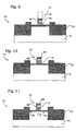
- Some poly 2 remains under the poly 3 and the photoresist, including under the high-k dielectric material if present. Since T OX - ⁇ T OX > X STI + ⁇ X STI , poly 1 is not completely removed from the active region, as shown in Fig.
- FIG. 9 which is a cross-sectional view of the device structure shown in Fig. 8 rotated by ninety degrees to show the cross-section along the source/channel/drain of a flash memory transistor structure.
- the thickness of the remaining poly 1 should be independent of the CMP process.
- a highly selective etch is used to etch the remaining portion of the first polysilicon layer 16 that is not covered by photoresist.
- micro-trenching may be reduced, or eliminated.
- the remainder of poly 1 can be selectively removed without excessive removal of tunnel oxide layer 12 in the source and drain region.
- the photoresist is then removed leaving the flash memory gate structure 72 that comprises the remaining portions of poly 1, high-k dielectric material, and poly 3 over each active area, as shown in Fig. 10. Some poly 2 remains under the portion of poly 3 extending beyond the active region, which is not visible in Fig. 10.
- ion implantation may be used to form source and drain regions that are self-aligned to the gate structure.
- Poly 1, poly 2, and poly 3 are also converted to n+ or p+ polysilicon as is common in conventional processes.
- the flash memory gate structure may alternatively be doped prior to the gate electrode etch, and prior to the source and drain ion implant.
- the polysilicon gate may also be salicided. Several methods of polysilicon gate doping, silicide or self aligned processes, including salicide processes, may be applied to the present process.
- the flash memory gate structure 72 following doping is shown in Fig. 11, which also shows the implanted source and drain regions 76.
- the source and drain regions 76 are separated from each other by a gate stack comprising the tunnel oxide layer, the floating polysilicon gate, the high-k dielectric layer and the control gate.
Landscapes
- Non-Volatile Memory (AREA)
- Semiconductor Memories (AREA)
Abstract
Description
Claims (11)
- A method of making a flash memory cell comprising the steps of:forming a first polysilicon layer, which has a bottom surface and a top surface, overlying a substrate with a tunnel oxide layer interposed between the substrate and the first polysilicon layer;forming a trench through the first polysilicon layer, and into the substrate;forming a field oxide layer, having an upper surface, overlying the substrate to a thickness such that the upper surface of the field oxide layer within the trench is higher than the bottom surface of the first polysilicon layer;depositing a second polysilicon layer, having an upper surface, overlying the field oxide layer to a thickness such that the upper surface of the second polysilicon layer within the trench is lower than the top surface of the first polysilicon layer;depositing a sacrificial oxide layer over the second polysilicon layer;planarizing the second polysilicon layer, the field oxide layer, and the first polysilicon layer; andstopping the step of planarizing at the top surface of the first polysilicon layer and the upper surface of the second polysilicon layer;depositing a high-k dielectric material overlying the first polysilicon layer; anddepositing a third polysilicon layer overlying the high-k dielectric material.
- The method of claim 1, wherein the field oxide layer is formed by growing a thin thermal oxide and then depositing the remainder of the oxide using a CVD process, or sputtering.
- The method of claim 1, wherein the tunnel oxide layer is silicon dioxide.
- The method of claim 1, wherein the high-k dielectric material is hafnium oxide or zirconium oxide.
- The method of claim 3, further comprising the steps of:depositing and patterning photoresist to define a gate structure;selectively etching the third polysilicon layer, the high-k dielectric material, the second polysilicon layer, and the first polysilicon layer; andstopping the selective etching after the removal of exposed regions of the second polysilicon layer, whereby a thin layer of exposed first polysilicon layer remains.
- The method of claim 5, further comprising the step of selectively etching the remaining exposed first polysilicon layer using a highly selective etch, whereby the remaining exposed first polysilicon layer is removed without excess removal of the underlying tunnel oxide layer.
- The method of claim 1, further comprising the steps of:applying and patterning photoresist overlying the high-k dielectric material prior to depositing the third polysilicon layer; and removing the high-k dielectric material from areas where non-memory transistors are to be formed.
- The method of claim 7, further comprising the steps of:depositing a sacrificial polysilicon layer over the high-k dielectric material prior to applying and patterning the photoresist; and removing the sacrificial polysilicon layer from the areas where the non-memory transistors are to be formed.
- A flash memory cell structure comprising a tunnel oxide layer overlying a substrate, a floating polysilicon gate overlying the tunnel oxide layer, a high-k dielectric layer overlying the floating polysilicon gate, and a control gate overlying the high-k dielectric layer.
- The flash memory cell structure of claim 9, wherein the high-k dielectric layer is hafnium oxide or zirconium oxide.
- The flash memory cell structure of claim 9, further comprising a source region and a drain region separated from each other by a gate stack comprising the tunnel oxide layer, the floating polysilicon gate, the high-k dielectric layer and the control gate.
Applications Claiming Priority (2)
| Application Number | Priority Date | Filing Date | Title |
|---|---|---|---|
| US622667 | 1984-06-20 | ||
| US10/622,667 US6858514B2 (en) | 2002-03-29 | 2003-07-17 | Low power flash memory cell and method |
Publications (2)
| Publication Number | Publication Date |
|---|---|
| EP1498945A2 true EP1498945A2 (en) | 2005-01-19 |
| EP1498945A3 EP1498945A3 (en) | 2007-09-26 |
Family
ID=33477133
Family Applications (1)
| Application Number | Title | Priority Date | Filing Date |
|---|---|---|---|
| EP04016720A Withdrawn EP1498945A3 (en) | 2003-07-17 | 2004-07-15 | Low power flash memory cell and method |
Country Status (6)
| Country | Link |
|---|---|
| US (2) | US6858514B2 (en) |
| EP (1) | EP1498945A3 (en) |
| JP (1) | JP2005039280A (en) |
| KR (1) | KR100587186B1 (en) |
| CN (1) | CN100353526C (en) |
| TW (1) | TWI248171B (en) |
Families Citing this family (12)
| Publication number | Priority date | Publication date | Assignee | Title |
|---|---|---|---|---|
| US6429481B1 (en) * | 1997-11-14 | 2002-08-06 | Fairchild Semiconductor Corporation | Field effect transistor and method of its manufacture |
| US7012021B2 (en) * | 2004-01-29 | 2006-03-14 | Taiwan Semiconductor Mfg | Method for end point detection polysilicon chemical mechanical polishing in an anti-fuse memory device |
| US7323424B2 (en) * | 2004-06-29 | 2008-01-29 | Micron Technology, Inc. | Semiconductor constructions comprising cerium oxide and titanium oxide |
| JP2006351881A (en) * | 2005-06-16 | 2006-12-28 | Toshiba Corp | Semiconductor memory device and manufacturing method of semiconductor memory device |
| US20070056925A1 (en) * | 2005-09-09 | 2007-03-15 | Lam Research Corporation | Selective etch of films with high dielectric constant with H2 addition |
| JP4933792B2 (en) * | 2006-02-15 | 2012-05-16 | 三菱電機株式会社 | Semiconductor device and manufacturing method thereof |
| US8183161B2 (en) * | 2006-09-12 | 2012-05-22 | Tokyo Electron Limited | Method and system for dry etching a hafnium containing material |
| US7879663B2 (en) * | 2007-03-08 | 2011-02-01 | Freescale Semiconductor, Inc. | Trench formation in a semiconductor material |
| KR100937818B1 (en) * | 2007-08-20 | 2010-01-20 | 주식회사 하이닉스반도체 | Flash memory device and manufacturing method thereof |
| US9029255B2 (en) * | 2012-08-24 | 2015-05-12 | Nanya Technology Corporation | Semiconductor device and fabrication method therof |
| CN105261622B (en) * | 2014-06-03 | 2017-12-22 | 上海丽恒光微电子科技有限公司 | A kind of manufacture method of imaging detector |
| CN106057669A (en) * | 2016-06-24 | 2016-10-26 | 上海华虹宏力半导体制造有限公司 | IGBT terminal field oxide technique |
Family Cites Families (18)
| Publication number | Priority date | Publication date | Assignee | Title |
|---|---|---|---|---|
| TW347567B (en) * | 1996-03-22 | 1998-12-11 | Philips Eloctronics N V | Semiconductor device and method of manufacturing a semiconductor device |
| US6008112A (en) * | 1998-01-08 | 1999-12-28 | International Business Machines Corporation | Method for planarized self-aligned floating gate to isolation |
| KR100699608B1 (en) * | 1999-03-09 | 2007-03-23 | 코닌클리즈케 필립스 일렉트로닉스 엔.브이. | Semiconductor Devices Including Nonvolatile Memory |
| US6232635B1 (en) * | 2000-04-06 | 2001-05-15 | Advanced Micro Devices, Inc. | Method to fabricate a high coupling flash cell with less silicide seam problem |
| US6624022B1 (en) * | 2000-08-29 | 2003-09-23 | Micron Technology, Inc. | Method of forming FLASH memory |
| TW494544B (en) * | 2001-05-03 | 2002-07-11 | Shr Min | Structure and manufacture method of non-volatile memory |
| CN1192439C (en) * | 2001-06-25 | 2005-03-09 | 旺宏电子股份有限公司 | Flash memory structure |
| KR20030002710A (en) * | 2001-06-29 | 2003-01-09 | 주식회사 하이닉스반도체 | Method for manufacturing a flash memory device |
| KR100393229B1 (en) * | 2001-08-11 | 2003-07-31 | 삼성전자주식회사 | Method of manufacturing non-volatile memory device including self-aligned gate structure and device by the same |
| KR20030043499A (en) * | 2001-11-28 | 2003-06-02 | 주식회사 하이닉스반도체 | Method of manufacturing a flash memory cell |
| US6674138B1 (en) * | 2001-12-31 | 2004-01-06 | Advanced Micro Devices, Inc. | Use of high-k dielectric materials in modified ONO structure for semiconductor devices |
| US6642573B1 (en) * | 2002-03-13 | 2003-11-04 | Advanced Micro Devices, Inc. | Use of high-K dielectric material in modified ONO structure for semiconductor devices |
| JP2003318287A (en) * | 2002-04-19 | 2003-11-07 | Hitachi Ltd | Nonvolatile semiconductor memory device and method of manufacturing the same |
| US6548855B1 (en) * | 2002-05-16 | 2003-04-15 | Advanced Micro Devices, Inc. | Non-volatile memory dielectric as charge pump dielectric |
| US6682973B1 (en) * | 2002-05-16 | 2004-01-27 | Advanced Micro Devices, Inc. | Formation of well-controlled thin SiO, SiN, SiON layer for multilayer high-K dielectric applications |
| US6617639B1 (en) * | 2002-06-21 | 2003-09-09 | Advanced Micro Devices, Inc. | Use of high-K dielectric material for ONO and tunnel oxide to improve floating gate flash memory coupling |
| US6753570B1 (en) * | 2002-08-20 | 2004-06-22 | Advanced Micro Devices, Inc. | Memory device and method of making |
| US7122415B2 (en) * | 2002-09-12 | 2006-10-17 | Promos Technologies, Inc. | Atomic layer deposition of interpoly oxides in a non-volatile memory device |
-
2003
- 2003-07-17 US US10/622,667 patent/US6858514B2/en not_active Expired - Lifetime
-
2004
- 2004-07-15 EP EP04016720A patent/EP1498945A3/en not_active Withdrawn
- 2004-07-16 KR KR1020040055777A patent/KR100587186B1/en not_active Expired - Fee Related
- 2004-07-16 JP JP2004210860A patent/JP2005039280A/en active Pending
- 2004-07-16 TW TW093121384A patent/TWI248171B/en not_active IP Right Cessation
- 2004-07-19 CN CNB200410069696XA patent/CN100353526C/en not_active Expired - Fee Related
- 2004-10-29 US US10/976,596 patent/US20050088898A1/en not_active Abandoned
Also Published As
| Publication number | Publication date |
|---|---|
| JP2005039280A (en) | 2005-02-10 |
| US20050088898A1 (en) | 2005-04-28 |
| KR100587186B1 (en) | 2006-06-08 |
| US6858514B2 (en) | 2005-02-22 |
| KR20050009246A (en) | 2005-01-24 |
| TW200525705A (en) | 2005-08-01 |
| US20040140504A1 (en) | 2004-07-22 |
| CN100353526C (en) | 2007-12-05 |
| EP1498945A3 (en) | 2007-09-26 |
| CN1591832A (en) | 2005-03-09 |
| TWI248171B (en) | 2006-01-21 |
Similar Documents
| Publication | Publication Date | Title |
|---|---|---|
| US8053823B2 (en) | Simplified buried plate structure and process for semiconductor-on-insulator chip | |
| EP3371812B1 (en) | Integration of metal floating gate in non-volatile memory | |
| US6703655B2 (en) | Ferroelectric memory transistor | |
| US6858514B2 (en) | Low power flash memory cell and method | |
| US6716691B1 (en) | Self-aligned shallow trench isolation process having improved polysilicon gate thickness control | |
| TWI794807B (en) | Method of making memory cells, high voltage devices and logic devices on a substrate | |
| CN113838853B (en) | Method of manufacturing memory cell, high voltage device and logic device on substrate | |
| US6627510B1 (en) | Method of making self-aligned shallow trench isolation | |
| US6673664B2 (en) | Method of making a self-aligned ferroelectric memory transistor | |
| US11968829B2 (en) | Method of forming memory cells, high voltage devices and logic devices on a semiconductor substrate | |
| US11737266B2 (en) | Method of forming a semiconductor device with memory cells, high voltage devices and logic devices on a substrate | |
| US6087696A (en) | Stacked tunneling dielectric technology for improving data retention of EEPROM cell | |
| US8354704B2 (en) | Method for fabricating an enlarged oxide-nitride-oxide structure for NAND flash memory semiconductor devices | |
| US6991942B1 (en) | MFIS ferroelectric memory array on SOI and method of making same | |
| CN118696614A (en) | Method for forming a semiconductor device having a memory cell, a high voltage device, and a logic device on a substrate using a dummy region | |
| KR20230110363A (en) | Method of forming a semiconductor device having memory cells, high voltage devices and logic devices on a substrate | |
| TWI784635B (en) | Method of making memory cells, high voltage devices and logic devices on a substrate with silicide on conductive blocks | |
| US6787842B1 (en) | Method for operating a stacked gate field effect transistor (FET) device |
Legal Events
| Date | Code | Title | Description |
|---|---|---|---|
| PUAI | Public reference made under article 153(3) epc to a published international application that has entered the european phase |
Free format text: ORIGINAL CODE: 0009012 |
|
| AK | Designated contracting states |
Kind code of ref document: A2 Designated state(s): AT BE BG CH CY CZ DE DK EE ES FI FR GB GR HU IE IT LI LU MC NL PL PT RO SE SI SK TR |
|
| AX | Request for extension of the european patent |
Extension state: AL HR LT LV MK |
|
| PUAL | Search report despatched |
Free format text: ORIGINAL CODE: 0009013 |
|
| AK | Designated contracting states |
Kind code of ref document: A3 Designated state(s): AT BE BG CH CY CZ DE DK EE ES FI FR GB GR HU IE IT LI LU MC NL PL PT RO SE SI SK TR |
|
| AX | Request for extension of the european patent |
Extension state: AL HR LT LV MK |
|
| AKX | Designation fees paid | ||
| STAA | Information on the status of an ep patent application or granted ep patent |
Free format text: STATUS: THE APPLICATION IS DEEMED TO BE WITHDRAWN |
|
| 18D | Application deemed to be withdrawn |
Effective date: 20080327 |
|
| REG | Reference to a national code |
Ref country code: DE Ref legal event code: 8566 |