EP1498929A2 - Magnetic lens - Google Patents
Magnetic lens Download PDFInfo
- Publication number
- EP1498929A2 EP1498929A2 EP04076906A EP04076906A EP1498929A2 EP 1498929 A2 EP1498929 A2 EP 1498929A2 EP 04076906 A EP04076906 A EP 04076906A EP 04076906 A EP04076906 A EP 04076906A EP 1498929 A2 EP1498929 A2 EP 1498929A2
- Authority
- EP
- European Patent Office
- Prior art keywords
- coil
- lens
- section
- sections
- coil section
- Prior art date
- Legal status (The legal status is an assumption and is not a legal conclusion. Google has not performed a legal analysis and makes no representation as to the accuracy of the status listed.)
- Granted
Links
Images


Classifications
-
- H—ELECTRICITY
- H01—ELECTRIC ELEMENTS
- H01J—ELECTRIC DISCHARGE TUBES OR DISCHARGE LAMPS
- H01J37/00—Discharge tubes with provision for introducing objects or material to be exposed to the discharge, e.g. for the purpose of examination or processing thereof
- H01J37/02—Details
- H01J37/04—Arrangements of electrodes and associated parts for generating or controlling the discharge, e.g. electron-optical arrangement or ion-optical arrangement
- H01J37/06—Electron sources; Electron guns
- H01J37/07—Eliminating deleterious effects due to thermal effects or electric or magnetic fields
-
- H—ELECTRICITY
- H01—ELECTRIC ELEMENTS
- H01J—ELECTRIC DISCHARGE TUBES OR DISCHARGE LAMPS
- H01J37/00—Discharge tubes with provision for introducing objects or material to be exposed to the discharge, e.g. for the purpose of examination or processing thereof
- H01J37/02—Details
- H01J37/04—Arrangements of electrodes and associated parts for generating or controlling the discharge, e.g. electron-optical arrangement or ion-optical arrangement
- H01J37/10—Lenses
- H01J37/14—Lenses magnetic
- H01J37/141—Electromagnetic lenses
-
- H—ELECTRICITY
- H01—ELECTRIC ELEMENTS
- H01J—ELECTRIC DISCHARGE TUBES OR DISCHARGE LAMPS
- H01J37/00—Discharge tubes with provision for introducing objects or material to be exposed to the discharge, e.g. for the purpose of examination or processing thereof
- H01J37/26—Electron or ion microscopes; Electron or ion diffraction tubes
- H01J37/28—Electron or ion microscopes; Electron or ion diffraction tubes with scanning beams
Definitions
- the present invention generally relates to a magnetic lens and, in particular, relates to a magnetic lens having thermal power dissipation independent of the strength of its magnetic field.
- Magnetic lenses are generally known and are often employed to focus a beam of charged particles e.g., electrons.
- a magnetic lens is useful as an objective, or final focusing lens. That is, the objective magnetic lens is the last focusing element prior to the beam impinging on the sample.
- the stability of the beam position as affected by the magnetic lens is quite critical to achieve an accurate characterization of small features on the sample.
- Such magnetic lenses are also often employed in e.g. Dual Beam systems.
- a Dual Beam system employs two beams of charged particles: one of these beams resembles the beam of an electron microscope, while the other beam can be e.g. an ion beam.
- the ion beam enables removal of material from the sample or deposition of material onto the sample.
- a magnetic lens can be used for the focusing of one of the beams, or two magnetic lenses can be used for the focusing of both beams.
- FIG. 1 is a cross-sectional, schematic drawing of a conventional magnetic lens assembly 100.
- Lens assembly 100 includes upper section 110 (which comprises an electron detector assembly), coil 115, and pole assembly 120, which includes upper pole piece 122, outer pole piece 124, inner pole piece 126, cooling ring 127, and insulator 129. Substantially collaring the ring-shaped coil 115, the pole pieces form a magnetic circuit around the coil for carrying magnetic flux when current flows through the coil.
- An air gap 131 proximal to the sample to be analyzed is disposed between the inner and outer pole pieces 124, 126.
- the centerline of the lens corresponding to the beam path is indicated at 105.
- the primary electrons are focused by the magnetic field B at the end of the lens near the air gap. Because the air gap 131 has significantly higher reluctance than the combined pole pieces, "fringing" occurs at the air gap causing the magnetic field B to bow, as shown, toward the sample in a desired annular shape for focusing incoming
- One feature of conventional analytical instruments employing an electron beam is that the energy of the electron beam is variable over a range of energies consistent with the range of materials to be characterized.
- the energy of the electron beam determines the depth of penetration and the range of Auger excitation of the atoms of the sample. Since the energy necessary to produce Auger electrons varies from atom to atom, a beam generator, to be effective, should be capable of producing electrons of various energies.
- the beam energy should be variable when the sample under analysis is an insulator because if the beam energy is high enough, the sample can become electrostatically charged. Such charging can be avoided by reducing the beam energy, sometimes to as low as 0.5 keV.
- the energy of the charged particle beam must be quite high, for example, on the order of about 30 keV.
- the energy of the electron beam should be variable over a broad energy range.
- the strength of the lens magnetic field typically must also be adjusted in order to ensure that the beam having the changed energy remains focused on the same point of the sample as the beam of previous energy.
- the magnitude of the magnetic field generated by the lens 100 is proportional to the number of coil-turns multiplied by the current in the coil 115 (measured in Amp-turns, At).
- the current in the coil By changing the current in the coil, one can vary the value of the magnetic field to match the energy of the beam.
- the lens coil is typically made of wire, which has electrical resistance, electrical power (heat) is generated in the coil.
- the amount of power P R ⁇ I 2 ).
- 1140 Amp-turns may be required. This can translate to about 15.5 W, which is a significant amount of heat, especially to be dissipated in the confined environment of a magnetic lens coil.
- the overall lens field strength is minimized when their magnitudes are the same, while the overall field strength increases as the difference between the individual current magnitudes increases, but the power generated by each coil is simply a function of the magnitude of its current squared.
- the generated power can be held constant while the effective lens magnetic field strength is varied.
- one drawback with this approach is that the overall response of the magnetic lens is fairly slow. That is, in order to attain the desired range of magnetic field strengths, both coils have a significant number of turns thereby giving them relatively large self-inductances. In fact, they can be large enough to inhibit field strength changes that are fast enough for such practices as dynamic focusing.
- a magnetic lens in one embodiment, can generate a substantially constant amount of average heat power over a preselected range of resultant magnetic field strengths.
- the lens is configured to do this with multiple, asymmetric (different turns) coil sections that can produce a range of desired field strengths, and at the same time, maintain a sufficiently constant temperature signature when the average total power is maintained constant thereby eliminating unreasonable delays in lens operation when the resultant field strength is changed over the operating range of field strengths.
- the asymmetric lens structure allows for the smaller coil to be made with less relative inductance thereby making it more responsive and amenable for AC signal driving and thus dynamic focusing applications if desired.
- a magnetic lens is now provided that can produce a range of magnetic beam-focusing field strengths, implement dynamic focusing, and not impose unreasonable delay for thermal stabilization between changes in magnetic field strength.
- FIG. 1 is a cross-sectional, schematic view of a prior art magnetic lens.
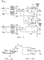
- FIG. 2 is a schematic view of a scanning electron microscope utilizing an embodiment of a magnetic lens of the present invention.
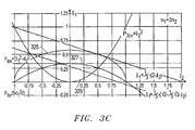
- FIGS. 3A-3C show constant power graphs for different multi-coil lens structures of the present invention.
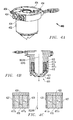
- FIG. 4A is a perspective view of one embodiment of a multi-coil lens assembly of the present invention.
- FIG. 4B is a cross-sectional view of the multi-coil lens of FIG. 4A highlighting the lens and pole assemblies.
- FIG. 4C is a block diagram of a coil assembly of the multi-coil lens of FIGS. 4A and 4B.
- FIG. 5 is an electrical schematic diagram of a circuit for driving the multi-coil assembly of FIGS. 4A-4C.
- FIG. 6A is a block diagram of an SEM beam length for different scan angles in an SEM.
- FIG. 6B is a top view of the block diagram of FIG. 6A taken along lines 6B-6B.
- the present invention provides improved multi-coil designs for magnetic lens applications.
- the improved lens coil is not only capable of dissipating substantially constant power over a range of operating magnetic field strengths, but also, it is responsive enough to be driven with a modulated current for dynamic focusing applications.
- the multi-coil lens may be used in a variety of applications, it is well suited as an objective lens for a scanning electron microscope ("SEM") in a dual beam system because its magnetic field strength can be adjusted without requiring excessive set-up time for thermal stabilization.
- SEM scanning electron microscope
- FIG. 2 schematically shows an SEM column 200 employing one embodiment of a multi-coil magnetic lens of the present invention.
- the SEM 200 provides a magnified image of a sample 202. It generally includes column housing 205, electron beam source 220, electrostatic alignment electrodes 230, aperture 235, blank beam dump device 237, multi-coil objective lens assembly 240, deflector 245, mirror electrode 247, light pipe 249, and "suck" tube 251.
- the electron beam source 220 includes electron source 222 and beam limiting aperture 224, which limits the outer portion of the electron beam for reducing optical aberrations.
- the electron beam source generates an electron beam that is directed down the central axis of the column toward sample 202.
- the blank beam dump 237 is connected to an electrometer for controlling and monitoring the size of the electron beam current applied to the sample 202.
- the beam is aligned toward the center axis with electrostatic alignment electrodes 230 and electrostatic deflectors 245, which also steer the beam for scanning the sample.
- the alignment electrodes incorporate electrostatic quadrupoles, which can be individually driven, for aligning the beam.
- the deflector 245 utilizes electrostatic octopoles that are individually driven and are also used for image shift and stagmation control.
- the multi-coil lens assembly 240 comprises a bi-furcated primary coil with an inner-disposed, smaller second coil for, among other things, generating a dynamic focusing field component.
- the multi-coil lens generates a desired magnetic field within a range of operational magnetic field strengths at substantially constant power dissipation.
- the lens assembly also includes cooling components to assist in maintaining the lens structure thermally stable.
- Objective lens 240 creates a focusing magnetic field proximal to the sample 202 at the downstream end of the lens assembly for focusing (e.g., de-magnifying) the electron beam just before it reaches the sample. Reflected electrons are then collected to a (not shown) fluorescent screen mounted on light pipe 249, where these reflected electrons generate photons. These photons pass through light pipe 249 for providing an image signal of the sample point being scanned.
- ion pumps 207 for evacuating the column
- a high voltage power supply 209 for energizing the electron source 220
- a chamber isolation valve 211 disposed midway down the column housing 205 for sealing the electron source 220 from the rest of the housing and/or operating environment when the SEM is not active.
- the valve includes a sensor for confirming that the valve is opened or closed.
- Column housing 205 also has a high vacuum vent 213 for evacuating the chamber, and electrical feed-throughs 215 for electrically connecting the various components through the sealed vacuum housing.
- a multi-coil magnetic lens has two or more coils disposed about a common core. This results in the overall resultant lens field to be a sum of the constituent individual coil fields.
- the magnetic field in a coil is proportional to the coil current and the number of turns of the coil: B ⁇ n ⁇ I
- B is the magnetic field produced by the coil
- n is the number of coil turns
- I is the current in the coil.
- the coil temperatures are equal.
- the wire used in each coil is the same (i.e., same material, same diameter).
- the coil sections have the same mean diameters. (As will be demonstrated below, this can occur with a bi-furcated first coil and an inner-disposed second coil.)
- the following analysis pertains to a lens with two coils, S 1 and S 2 and assumes that both coils have the same mean diameter, wire parameters, and temperature.
- the total magnetic field and power generated in the coil are proportional to the sums of the individual coil section components, or: B II ⁇ n 1 ⁇ I 1 + n 2 ⁇ I 2 and P II ⁇ n 1 ⁇ I 1 2 + n 2 .I 2 2
- the magnetic field B 1 determined by uni-directional current I 1 in coil S 1 is augmented or offset by the magnetic field B 2 generated in the second coil, depending on the direction of I 2 , while the total power created by both sections is kept constant.
- Power of course, is a function of the constituent current magnitudes but is independent of their directions.
- Power density, D is defined as power per unit length of wire in a coil section. The power densities affect each coil's ability to sufficiently dissipate its power, relative to the other coil, and thereby maintain thermal stability. Accordingly, in this analysis, another self-imposed constraint is that each coil section should have the same maximum power density.
- the magnetic field range under these conditions is: ⁇ ((n 1 - n 2 )/n 2 ) - ⁇ (n 2 /n 1 ) ⁇ B IIc ⁇ ⁇ ((n 1 + n 2 ))/n 2 )
- Curve 307 shows the power, P 1cns , dissipated in the first coil
- curve 309 shows the power, P 2cns , dissipated in the second coil. Only the positive side of the constant power curve 305 is depicted because, again, the primary coil current, I 1 , is uni-directional. All points on curve 305 satisfy the stipulation of a normalized constant power of one.
- Curve 315 is the constant power curve for this case.
- Curve 317 shows the power, P 1cns , dissipated in the first coil section
- curve 309 shows the power, P 2cns , dissipated in the second coil.
- I 1 is uni-directional. All points on this curve satisfy the relation of a constant power of 1.
- Graph 327 shows the power, P 1cns , dissipated in the first coil section, and graph 329 shows the power, P 2cns , dissipated in the second coil.
- B II is equal to n 1 ⁇ I 1 + n 2 I 2 or 3 ⁇ ⁇ 2/3 - 1 ⁇ 1/ ⁇ 3. Accordingly, the magnetic field range for this multi-coil design is: ⁇ 2 - 1/ ⁇ 3 ⁇ B ⁇ 2, or 0.83.. ⁇ B ⁇ 2
- FIG. 4A shows one embodiment of a multi-coil lens housing 400, which includes a multi-coil lens assembly. Shown in this figure are housing casing 402 and input/output ports 404. The input and output ports 404 are used for providing power, control signal, and fluid connections to the multi-coil lens assembly and to a water-cooled heat dissipation mechanism used to dissipate heat away from the lens assembly.
- the multi-coil lens assembly comprises coil assembly 415, pole assembly 420, and coil cooling mechanism 425.
- the pole assembly 420 forms a collar around coil assembly 415 with an annular air gap at its lower portion to define a magnetic field ring for focusing an electron beam at the beam axis.
- Coil cooling mechanism 425 is mounted to the coil assembly 415 and pole assembly 420 to channel heat away from the coil assembly in order to improve thermal stability.
- Coil assembly 415 comprises a bi-furcated primary coil section 417 (S 1 ) and a secondary (or dynamic) coil section 419 (S 2 ).
- Primary coil section 417 is formed from two sub-sections: inner coil section 417a (S 1a ) and outer coil section 417b (S 1b ).
- Secondary coil section 419 is sandwiched between outer primary section 417b and inner primary section 417a, which is nearest to the beam axis.
- the three coil sections: 417a, 417b, and 419 are concentrically wound about a common axis that corresponds to the beam axis. In this embodiment, they use the same type of wire with the same wire diameter.
- the coil construction is conventional, except that the winding process is interrupted to make connections to the coil sections.
- Pole assembly 420 is similar to the pole assembly described in FIG. 1. It includes inner and outer pole pieces 421 and 423 to form a collar like structure about the "roll” shaped coil assembly 505.
- the pole section “collar” almost completely envelops the coil assembly 415 except at its underside where an air gap is formed to create the desired ring-shaped magnetic field pattern around the beam axis at the lower portion of the pole assembly 420.
- the pole pieces are made from a ferro-magnetic material to more efficiently conduct the magnetic flux and concentrate almost all of the generated mmf (magneto motive force) in the air gap.
- the heat dissipation mechanism 425 comprises a water-cooling jacket and has outer and inner thermally conductive covers 427 and 429, respectively.
- the coil sections are surrounded by the inner and outer covers 427, 429 to reduce thermal resistance from the coil sections to the water cooled portion.
- the heat dissipation mechanism 425 and covers 427, 429 are formed from a water-cooling jacket with copper side plates, but varieties of conventional heat dissipation structures will suffice, depending on the particular environment.
- the heat dissipation mechanism 425 is not required, but it will generally improve operation by increasing the thermal stability of the lens, especially when it is designed to remove heat in accordance with the power generated by the coil assembly 415. This adds to its ability to maintain a substantially constant temperature signature under constant average generated power conditions.
- a lens assembly is desired for handling beams ranging between 0.5 and 2 keV.
- the sectional turns ratio, S 1a :S 2 :S 1b is 8:6:8, which translates to a primary-to-dynamic coil turns ratio, N 1 /N 2 , equal to 2.67. Since the inductance of each coil section is proportional to the number of turns squared, the inductance of S 2 is at n 1 ⁇ 2.67 ⁇ n 2 is almost 1 order of magnitude less than the inductance of S 1 .
- this ratio is also well-suited for dynamic focusing (discussed below) because most of the current modulation can occur in the lower inductance, secondary coil 419, which is sufficiently responsive for modulating the dynamic signal at the field scan frequency.
- FIG. 5 shows one embodiment of a circuit 500 for electrically driving coil sections 417a, 417b, and 419.
- Circuit 500 generally includes D-to-A converters (DACs) 502A, 502B, 526A, 526B; analog summing amps 504, 524; analog difference amps 506, 522; 508, 514, 516; low-pass filters 509; coil sections 417a, 417b, 419; measuring resistors 510, 520; and feedback amplifiers 512 and 518.
- the circuit can be divided into two sections: one for driving the primary coil (417a, 417b) and the other for driving the secondary coil (419).
- the circuit for driving the primary coil 417 is initially discussed followed by a discussion of the circuitry for driving the secondary coil 419.
- a digital command signal, I 1 is input to the primary coil driver section for controlling the amount of current driven through the primary coil.
- I 1 is composed of a course component, I 1course , which is input to the DAC 502A, and a fine component, I 1fine , which is input to DAC 502B.
- DACs 502A and 502B output analog command signal components that are summed together at analog summing amplifier 504, which generates an overall I 1 current command signal: the sum of I 1course and I 1fine .
- the overall I 1 current command signal is fed into differential amp 506 as one of its inputs.
- the other input is a feedback signal from feedback amp 512.
- Difference amp 506 subtracts the feedback signal from the I 1 current command signal and provides the resulting difference signal at its output.
- the feedback signal is an amplified version of the voltage dropped across measuring resistor 510. Because resistor 510 is in series between coil sections 417a and 417b (the input impedance of feedback amp 512 is extremely high), the voltage across it corresponds directly to the current in the primary coil sections 417a, 417b.
- the gain of feedback amp 512 is set so that the feedback signal fed into differential amp 506 is appropriately comparable with the I 1 current command signal. Accordingly, while the I 1 command signal represents the desired primary coil current, the feedback signal corresponds to the actual, real-time primary coil current.
- the difference signal generated by differential amp 506 is a closed-loop, error signal that controls current drivers 508 and 514. The error signal causes the current drivers to force current through the primary coil sections in accordance with the value of command signal I 1 .
- Low-pass filters 509 are disposed in series between the current drivers 508, 514 and their associated primary coil sections 417a, 417b, respectively. In the depicted embodiment, they each include a choke 511 and a capacitor 513. Filters 509 (but primarily chokes 511) serve to counter the flyback voltages created by the primary coil, which are greater than those created in the secondary coil 419 because of its greater number of coil turns and thus higher inductance. Unfortunately, however, the external alternating, magnetic field from the secondary coil can induce a voltage in the chokes, which can cause undesired current to flow through the primary lens coil 417. To limit this problem, the following measures may be taken. A choke construction that is less sensitive such as a toroid can be used.
- Toroids are rather insensitive to in tangential external fields and are less sensitive than other designs in their radial directions.
- the disturbing external magnetic fields could also be diverted with a lower-reluctance shield or shunt such as an iron heatsink.
- toroid chokes could be mounted on iron heatsink plates.
- the use of separate, counteracting chokes can be employed. That is, they can be arranged so that their induced voltages are in opposite directions relative to their electrically conductive paths.
- Filters 509 each have a cut-off frequency sufficiently high (e.g., >20 Hz) to allow the primary coil current to be changed with reasonable responsiveness. Therefore, the values of chokes 511 and capacitors 513 should be set to meet this objective. In the depicted embodiment, the chokes 511 have an inductance that is about 10 times the inductance of primary coil 417.
- measuring resistor 520 is connected between coil section 419 and ground rather than being disposed between two coil sections. Because the input resistance to feedback amp 518 is very high, the resistor, in effect, is in series with coil section 419. Therefore, the voltage drop across resistor 520 accurately corresponds to the current in the secondary coil.
- circuit 500 serves to accurately and independently control the currents in the primary and secondary (dynamic) coil sections in response to input digital command signals, I 1 and I 2 .
- I 1 and I 2 may come, for example, from a controller or processor in the SEM. In one embodiment, they are controlled in accordance with the constant power constraints discussed above, with I 1 being uni-directional and I 2 being modulated for implementing dynamic focusing, as is discussed in the following section.
- SEM microscopes are typically used for examining properties of semiconductor wafers very accurately.
- the electron beam is not usually perpendicularly directed over the scan field on a sample to be scanned. Instead, it may be offset from the sample at an angle such as 45 degrees. (This is represented in FIGS. 6A and 6B.) This results in beam length differences from the beam source to the various points on the scan field being different from one point to another such that it introduces unacceptable errors if not compensated.
- FIG. 6A schematically shows a side view of a SEM 605 projecting beam 607 onto a scan field of a sample 602.
- FIG. 6B shows a top view of the same taken along lines 6B-6B of FIG. 6A.
- the beam length varies as it scans points in different locations along the Y-axis.
- the differences in beam distance D beam can vary from a minimal distance, D min , to a maximum distance, D max .
- the beam length distance along the Y axis from one side to the other may vary up to 25 ⁇ m.
- the beam distance also varies along the X-axis from the center out to the edges, but this difference is not as dramatic. These beam length differences cause the beam to be out of focus for many of the points on a scan field.
- the focus point deviations can be addressed in several ways.
- This latter method is known as dynamic focusing. It involves changing the magnetic field strength in real-time to compensate for beam length differences within each field scan.
- a dynamic signal with a shape and frequency corresponding to the beam length differences profile and scan field frequency is used.
- a ramp (or saw tooth) function is used for the dynamic signal.
- the ramp signal is at its minimal value when the beam source is closest to the scan points. As the beam scans "up" along the scan field in the Y direction, the ramp signal increases in accordance therewith.
- the saw tooth signal is at its maximum when the beam is directed to points along the farthest end of the scan field.
- the field is not adjusted for beam length differences along the X axis, but if desired, this of course could be done by modulating an appropriate second signal onto I 2 to account for these variations.
- the primary and secondary coil sections are driven in the following manner for implementing both constant average power and dynamic focusing.
- An adjustable DC current signal is input as I 1 for driving the primary coil 417, while I 2 comprises a periodically varying dynamic focusing component, I 2AC , modulated on an adjustable DC offset component, I 2DC (which may be any value including negative values, positive values, and 0) for driving the secondary coil section 419.
- I 2AC periodically varying dynamic focusing component
- I 2DC which may be any value including negative values, positive values, and 0
- the average total generated power is kept substantially constant, while the real-time power is not necessarily constant for any two points in time.
- the value of I 1 is not changed in real-time according to a constant power function to compensate for the changes in I 2 attributable to its dynamic AC component because it is assumed that the dynamic component is "fast" enough such that the RMS (root mean squared) value of I 2 (I 2rms ), can be used as a static I 2 value for a given field strength in setting I 1 and I 2 in adherence to the constant power function. In most cases, this is sufficient to maintain a substantially constant thermal signature throughout the lens assembly.
- the coils in the magnetic lens should preferably have sufficiently low inductance that the magnetic lens can be dynamically focused at the desired scan rate. For example, if a scan rate sufficiently high to produce clear video images is desired, a lower inductance is required than that required for a lower scan rate.
- Various embodiments of the inventive lens can support dynamic focusing when the electron beam has a scan or frame rate of as great as, or greater than, approximately 15 Hz, approximately 20 Hz, approximately 25 Hz, or approximately 30 Hz, depending on the configuration.
- a preferred embodiment supports dynamic focusing at conventional TV scan rates, i.e., 30 Hz scan rate or greater. This means that the coil should be able to produce a 30 Hz saw-tooth current signal at sufficient current magnitudes and recovery intervals.
- a multi-coil lens as described above has the following characteristics: Total number of turns: 1232 Turns ratio's n 1 :n 2 :n 1 8 : 6 : 8 Ampere turns 1140 At Mean diameter 80 mm Dynamic focus requirement ( ⁇ z focus ): ⁇ 25 ⁇ m Z focus ⁇ 2.3 mm Moreover, the acceleration voltage of the electron beam in an SEM must be allowed to quickly changed (interruption less than one minute) over a range of operating voltages from 500V to 2kV. For the same focus point, this results in a required change in magnetic field from 570 to 1140 amp-turns (a change of a factor of two), and hence a variation in dissipated power of a factor 4. These parameters were met by implementing the following measures.
- a circular symmetric construction was employed.
- the objective coil was cooled with a water-cooling body having thermally conductive side covers, and it was insulated from the SEM housing.
- the constant power dissipation and constant power density techniques described above were also used.
- a dynamic focusing saw tooth signal was driven into the secondary coil to account for a beam distance change of 20 ⁇ m ( ⁇ 1% working depth of 2.3 mm).
- the nominal working distance is 2 mm.
- the present invention is certainly not limited to a coil assembly with a bi-furcated primary coil section, inner-sandwiched second coil section, and the presented cooling mechanism.
- a coil assembly with a bi-furcated primary coil section, inner-sandwiched second coil section, and the presented cooling mechanism.
- These are examples of structures for achieving a thermally stable lens with asymmetric coil sections that can maintain a substantially constant temperature signature under substantially constant average power conditions, but they are not required. From the teachings and suggestions herein, persons of skill will recognize different structures using combinations of techniques taught in this disclosure to achieve suitable thermal stability.
Landscapes
- Chemical & Material Sciences (AREA)
- Analytical Chemistry (AREA)
- Physics & Mathematics (AREA)
- Electromagnetism (AREA)
- Electron Beam Exposure (AREA)
- Lens Barrels (AREA)
Abstract
Description
1-1/√2 < B < √3
Because n1 has three times as many turns as n2, coil S1, without any constraints, would have a smaller maximum power density than S2. Therefore, to comply with the criteria that the coil sections should have the same maximum power densities, their power densities are constrained to D1max, (which is at I2 = 0. Thus, the maximum power density for S1 is 1/√3. Therefore, the minimal magnetic field, BII, occurs at I2 = -1/√3. This corresponds to I1 equal to 1 - 1/3 = 2/3. At this point, BII is equal to n1 ·I1 + n2I2 or 3 · √2/3 - 1 · 1/√3. Accordingly, the magnetic field range for this multi-coil design is:
| Total number of turns: | 1232 |
| Turns ratio, n1a:n2:n1b | 8:6:8 |
| Actual coil turns, S1a:S2:S1b | 448:336:448 |
| Diameter Cu wire: | 0.63 mm |
| Number of ampere turns | 1140 (A·t) |
| Total resistance | 18Ω |
| Total dissipated power | ca 15.5 W |
| B range (normalized) | 0.64 < B < 1.915 |
| B range (actual) | 0.3546 < B < 2.82 |
| Current at the maximum magnetic field (I1 = I2) | 0.93 A |
| I1max | 1.085 A |
| I2max | -1.085 A |
| Total number of turns: | 1232 |
| Turns ratio's n1:n2:n1 | 8 : 6 : 8 |
| Ampere turns | 1140 At |
| Mean diameter | 80 mm |
| Dynamic focus requirement (Δzfocus): | ≈25 µm |
| Zfocus | ≈2.3 mm |
Number of turns section 2:
Claims (22)
- A magnetic lens comprising:wherein the secondary coil section is sufficiently responsive for implementing dynamic focusing when it is driven with a dynamic focusing current.primary and secondary coil sections each having coil turns for generating additive magnetic fields thereby forming a resultant beam focusing field, the primary coil section having a larger number of coil turns than the secondary coil section, the sections being configured to have a substantially constant thermal signature when operated with their combined average generated power being substantially constant over an operational range of resultant field strengths;
- The lens of claim 1 further comprising a choke connected in series with the primary coil section for countering adverse flyback voltage effects.
- The lens of claim 1, wherein the primary coil section is divided into first and second coil sub-sections with the secondary coil section disposed between said first and second primary coil sub-sections.
- The lens of claim 3, wherein the first and second primary coil sub-sections have substantially the same number of coil turns.
- The lens of claim 1 further comprising a cooling body mounted at a common end of the primary and secondary coil sections.
- The lens of claim 5, further comprising thermally conductive covers thermally connecting one or more areas of the coil sections to the cooling body.
- The lens of claim 1, wherein the electrically conductive coil turns are implemented with wire.
- The lens of claim 7, wherein the wire in the primary and secondary coil sections have substantially the same resistivity characteristics.
- The lens of claim 1, wherein the ratio of coil turns in the primary coil section to turns in the secondary coil section is greater than or equal to 2 to 1.
- The lens of claim 1, wherein the secondary coil section is sufficiently responsive for implementing dynamic focusing as the beam is scanned at approximately 30 Hz frame rate or greater.
- A SEM having a multi-coil lens in accordance with the magnetic lens described in claim 1.
- A method for generating a beam focusing magnetic field in a SEM, comprising:providing first and second coil sections configured to produce additive field components, the field components adding to form a resultant beam focusing field, wherein the first coil section has a larger number of coil turns than the second coil section;driving the first coil section to generate the first section field component; anddriving the second coil section to generate the second section field component, the second coil section being driven with an AC signal component, wherein the first and second coil sections are driven to (i) produce a desired resultant field strength from a range of available field strengths, and (ii) generate substantially the same total average power over the range of available field strengths thereby maintaining a sufficiently constant thermal signature in the coil sections to allow for the resultant field strength to be changed without requiring a delay for thermal stabilization.
- The method of claim 11, further comprising dynamically modulating a current signal for driving the second coil section to change the resultant field strength in accordance with changes in beam distance to a scan point.
- The method of claim 13 in which the current is modulated by a sawtooth signal at approximately 30 Hz frame rate or greater.
- The method of claim 11, wherein the first coil section is driven in only one direction, while the second section is driven in more than one direction.
- The method of claim 11, wherein both the first and second coil sections are driven to have the same maximum allowed power densities.
- A dual beam system having a controller for controlling a magnetic lens in an SEM, said controller accessible to instructions that when executed by the controller cause it to control the magnetic lens to produce a resultant beam focusing magnetic field in accordance with the method of claim 11.
- A dual beam system having a charged particle column comprising:a charged particle source assembly;a holder for receiving a sample to be irradiated by said charged particle source;a magnetic lens disposed between said charged particle source and said holder for focusing a charged particle beam emitted from said charged particle source, the magnetic lens including a first coil section having coil turns for generating a first section field component and a second coil section having coil turns for generating a second section field component, said coil sections being configured to produce a resultant beam focusing field that is the sum of said first and second section field components, wherein the first coil section has a greater number of turns than the second coil section resulting in the second coil section being more responsive than the first coil section; andcircuitry connected to said first and second coil sections, said circuitry adapted to drive the first and second coil sections to generate a selected resultant beam focusing field from a range of available resultant fields, wherein the total average power produced by both coil sections is substantially constant throughout the range of available resultant fields, the coil sections being configured to have a substantially constant temperature signature throughout the coil sections when their total average power is substantially constant, wherein most current change in the coil sections for changing the resultant beam focusing field occurs in the second coil section.
- The dual beam system of claim 16, wherein the charged particle column is offset from the holder at an angle thereby having different beam distances from the charged particle source to various scan points on the sample, the circuitry additionally driving the second coil section with a dynamic focusing current component to compensate for said beam length differences.
- The system of claim 16, wherein the first coil section has first and second subsection components sandwiched around the second coil section.
- The system of claim 16, wherein the first and second coil section turns are at least partially bi-flair wound together.
- The system of claim 16, wherein the charged particle column is a SEM.
Applications Claiming Priority (2)
| Application Number | Priority Date | Filing Date | Title |
|---|---|---|---|
| US10/621,103 US6852982B1 (en) | 2003-07-14 | 2003-07-14 | Magnetic lens |
| US621103 | 2003-07-14 |
Publications (3)
| Publication Number | Publication Date |
|---|---|
| EP1498929A2 true EP1498929A2 (en) | 2005-01-19 |
| EP1498929A3 EP1498929A3 (en) | 2009-09-02 |
| EP1498929B1 EP1498929B1 (en) | 2011-12-14 |
Family
ID=33477108
Family Applications (1)
| Application Number | Title | Priority Date | Filing Date |
|---|---|---|---|
| EP04076906A Expired - Lifetime EP1498929B1 (en) | 2003-07-14 | 2004-07-01 | Magnetic lens |
Country Status (3)
| Country | Link |
|---|---|
| US (1) | US6852982B1 (en) |
| EP (1) | EP1498929B1 (en) |
| JP (2) | JP4789436B2 (en) |
Cited By (4)
| Publication number | Priority date | Publication date | Assignee | Title |
|---|---|---|---|---|
| EP1501115A3 (en) * | 2003-07-14 | 2007-09-05 | FEI Company | Dual beam system |
| WO2009100877A1 (en) * | 2008-02-15 | 2009-08-20 | PTR Präzisionstechnik GmbH | An electron beam unit and method for adjusting electron beams generated by an electron beam unit |
| DE102016225463A1 (en) | 2016-12-19 | 2018-06-21 | E.G.O. Elektro-Gerätebau GmbH | Induction hob |
| US10622184B2 (en) | 2005-11-28 | 2020-04-14 | Carl Zeiss Microscopy Gmbh | Objective lens arrangement usable in particle-optical systems |
Families Citing this family (22)
| Publication number | Priority date | Publication date | Assignee | Title |
|---|---|---|---|---|
| US7078994B2 (en) * | 2003-02-18 | 2006-07-18 | Glenn Henry Martin | Constant power and temperature coil |
| GB2418061B (en) * | 2004-09-03 | 2006-10-18 | Zeiss Carl Smt Ltd | Scanning particle beam instrument |
| US8159118B2 (en) | 2005-11-02 | 2012-04-17 | United Technologies Corporation | Electron gun |
| EP1970935B1 (en) * | 2007-03-14 | 2011-01-12 | ICT, Integrated Circuit Testing Gesellschaft für Halbleiterprüftechnik mbH | Lens coil cooling of a magnetic lens |
| JP4977509B2 (en) * | 2007-03-26 | 2012-07-18 | 株式会社日立ハイテクノロジーズ | Scanning electron microscope |
| JP5702552B2 (en) * | 2009-05-28 | 2015-04-15 | エフ イー アイ カンパニFei Company | Control method of dual beam system |
| GB2478134B (en) * | 2010-02-25 | 2012-01-11 | Micro Materials Ltd | Heating in material testing apparatus |
| EP2609612B1 (en) * | 2010-08-27 | 2019-11-13 | GE Sensing & Inspection Technologies GmbH | Microfocus x-ray tube for a high-resolution x-ray apparatus |
| CN102386047B (en) * | 2011-11-08 | 2013-09-18 | 北京航空航天大学 | Objective lens coil for transmission electron microscope |
| EP2827357A1 (en) | 2013-07-18 | 2015-01-21 | Fei Company | Magnetic lens for focusing a beam of charged particles |
| JP2018174016A (en) * | 2015-07-29 | 2018-11-08 | 株式会社日立ハイテクノロジーズ | Charged particle beam equipment |
| US9818577B2 (en) | 2016-01-25 | 2017-11-14 | Applied Materials Israel Ltd. | Multi mode system with a dispersion X-ray detector |
| US10074513B2 (en) * | 2016-01-25 | 2018-09-11 | Applied Materials Israel Ltd. | Multi mode systems with retractable detectors |
| WO2017196996A1 (en) * | 2016-05-10 | 2017-11-16 | Reddy Sara Rani | Hygienic tissue |
| JP6954885B2 (en) | 2018-11-26 | 2021-10-27 | 日本電子株式会社 | Control method of charged particle beam device and charged particle beam device |
| DE102019127963A1 (en) * | 2019-10-16 | 2021-04-22 | Carl Zeiss Microscopy Gmbh | Particle beam system |
| DE102020114774B3 (en) | 2020-06-03 | 2021-09-23 | Carl Zeiss Microscopy Gmbh | Particle beam system |
| TW202220012A (en) | 2020-09-30 | 2022-05-16 | 德商卡爾蔡司多重掃描電子顯微鏡有限公司 | Multiple particle beam microscope and associated method with fast autofocus around an adjustable working distance |
| DE102020125534B3 (en) * | 2020-09-30 | 2021-12-02 | Carl Zeiss Multisem Gmbh | Multiple particle beam microscope and associated process with fast autofocus at an adjustable working distance |
| EP4113573A1 (en) | 2021-06-30 | 2023-01-04 | FEI Company | Method and system for studying samples using a scanning transmission charged particle microscope with reduced beam-induced sample damage |
| US11810749B2 (en) | 2021-12-06 | 2023-11-07 | Carl Zeiss Smt Gmbh | Charged particle beam system, method of operating a charged particle beam system, method of recording a plurality of images and computer programs for executing the methods |
| CN119480589B (en) * | 2025-01-15 | 2025-04-11 | 惠然科技有限公司 | Method and apparatus for maintaining objective lens constant temperature in charged particle beam system |
Family Cites Families (19)
| Publication number | Priority date | Publication date | Assignee | Title |
|---|---|---|---|---|
| NL129187C (en) * | 1962-06-25 | |||
| US4345152A (en) * | 1980-08-11 | 1982-08-17 | The Perkin-Elmer Corporation | Magnetic lens |
| JPS5981850A (en) * | 1982-11-02 | 1984-05-11 | Internatl Precision Inc | Electron lens |
| JPH0760657B2 (en) * | 1985-08-22 | 1995-06-28 | 株式会社日立製作所 | Electron beam exposure system |
| JPS6417364A (en) * | 1987-07-13 | 1989-01-20 | Mitsubishi Electric Corp | Electron beam device |
| JP2920390B2 (en) * | 1989-11-08 | 1999-07-19 | 株式会社日立製作所 | Electronic lens cooling system |
| US5206516A (en) * | 1991-04-29 | 1993-04-27 | International Business Machines Corporation | Low energy, steered ion beam deposition system having high current at low pressure |
| US6099394A (en) * | 1998-02-10 | 2000-08-08 | Rodel Holdings, Inc. | Polishing system having a multi-phase polishing substrate and methods relating thereto |
| US5435816A (en) * | 1993-01-14 | 1995-07-25 | Minnesota Mining And Manufacturing Company | Method of making an abrasive article |
| KR0165625B1 (en) * | 1993-06-02 | 1999-02-01 | 기타지마 요시토시 | Grinding tape and method of manufacturing the grinding tape |
| JPH08115696A (en) * | 1994-10-19 | 1996-05-07 | Jeol Ltd | Coil for electromagnet |
| US6051839A (en) * | 1996-06-07 | 2000-04-18 | Arch Development Corporation | Magnetic lens apparatus for use in high-resolution scanning electron microscopes and lithographic processes |
| US6036579A (en) * | 1997-01-13 | 2000-03-14 | Rodel Inc. | Polymeric polishing pad having photolithographically induced surface patterns(s) and methods relating thereto |
| JP3041600B2 (en) * | 1998-05-19 | 2000-05-15 | セイコーインスツルメンツ株式会社 | Complex charged particle beam device |
| WO2000043159A1 (en) * | 1999-01-21 | 2000-07-27 | Rodel Holdings, Inc. | Improved polishing pads and methods relating thereto |
| US6130432A (en) * | 1999-04-13 | 2000-10-10 | International Business Machines Corporation | Particle beam system with dynamic focusing |
| WO2001043920A1 (en) * | 1999-12-14 | 2001-06-21 | Rodel Holdings, Inc. | Method of manufacturing a polymer or polymer composite polishing pad |
| WO2001097245A2 (en) * | 2000-06-15 | 2001-12-20 | Kla-Tencor, Inc. | Sectored magnetic lens and method of use |
| US6679769B2 (en) * | 2000-09-19 | 2004-01-20 | Rodel Holdings, Inc | Polishing pad having an advantageous micro-texture and methods relating thereto |
-
2003
- 2003-07-14 US US10/621,103 patent/US6852982B1/en not_active Expired - Lifetime
-
2004
- 2004-07-01 EP EP04076906A patent/EP1498929B1/en not_active Expired - Lifetime
- 2004-07-14 JP JP2004207895A patent/JP4789436B2/en not_active Expired - Lifetime
-
2011
- 2011-05-10 JP JP2011105157A patent/JP2011151042A/en active Pending
Cited By (5)
| Publication number | Priority date | Publication date | Assignee | Title |
|---|---|---|---|---|
| EP1501115A3 (en) * | 2003-07-14 | 2007-09-05 | FEI Company | Dual beam system |
| US10622184B2 (en) | 2005-11-28 | 2020-04-14 | Carl Zeiss Microscopy Gmbh | Objective lens arrangement usable in particle-optical systems |
| US11527379B2 (en) | 2005-11-28 | 2022-12-13 | Carl Zeiss Microscopy Gmbh | Objective lens arrangement usable in particle-optical systems |
| WO2009100877A1 (en) * | 2008-02-15 | 2009-08-20 | PTR Präzisionstechnik GmbH | An electron beam unit and method for adjusting electron beams generated by an electron beam unit |
| DE102016225463A1 (en) | 2016-12-19 | 2018-06-21 | E.G.O. Elektro-Gerätebau GmbH | Induction hob |
Also Published As
| Publication number | Publication date |
|---|---|
| EP1498929A3 (en) | 2009-09-02 |
| JP4789436B2 (en) | 2011-10-12 |
| JP2011151042A (en) | 2011-08-04 |
| JP2005038857A (en) | 2005-02-10 |
| US6852982B1 (en) | 2005-02-08 |
| US20050012049A1 (en) | 2005-01-20 |
| EP1498929B1 (en) | 2011-12-14 |
Similar Documents
| Publication | Publication Date | Title |
|---|---|---|
| EP1498929B1 (en) | Magnetic lens | |
| US6423976B1 (en) | Ion implanter and a method of implanting ions | |
| US6723997B2 (en) | Aberration corrector for instrument utilizing charged-particle beam | |
| US7872240B2 (en) | Corrector for charged-particle beam aberration and charged-particle beam apparatus | |
| JP4676714B2 (en) | Particle optical device comprising a permanent magnetic lens and an electrostatic lens | |
| EP0251381A2 (en) | Magnetic lens system | |
| JP4133602B2 (en) | Aberration correction method in charged particle beam apparatus and charged particle beam apparatus | |
| TW201209877A (en) | Charged particle apparatus | |
| JP2009517816A (en) | Particle optics | |
| JPS6331896B2 (en) | ||
| KR19990028770A (en) | Correction apparatus for correcting lens aberrations in particle-optical devices | |
| US6696688B2 (en) | Apparatus for magnetically scanning and/or switching a charged-particle beam | |
| JP2004087460A (en) | Charged particle beam device with aberration correction device | |
| JP3899317B2 (en) | Deflection system for particle beam equipment | |
| JP4823995B2 (en) | Aberration correction type mass separator | |
| JP2007280966A (en) | Electro-optic lens device | |
| DE3901980C2 (en) | Multipole element and method for producing a multipole element | |
| JPH01319236A (en) | Field emission electron gun | |
| EP0596529B1 (en) | Electron lens | |
| JP2000517095A5 (en) | ||
| WO2020240861A1 (en) | Beam deflection device, aberration corrector, monochromator, and charged particle beam device | |
| RU2257690C2 (en) | Device for irradiation and method for correcting beam position | |
| WO2014030429A1 (en) | Charged particle beam device and objective lens | |
| JP2004199912A (en) | Aberration correction device in charged particle beam device | |
| JP3236472B2 (en) | Electromagnetic field superimposition type objective lens |
Legal Events
| Date | Code | Title | Description |
|---|---|---|---|
| PUAI | Public reference made under article 153(3) epc to a published international application that has entered the european phase |
Free format text: ORIGINAL CODE: 0009012 |
|
| 17P | Request for examination filed |
Effective date: 20040701 |
|
| AK | Designated contracting states |
Kind code of ref document: A2 Designated state(s): AT BE BG CH CY CZ DE DK EE ES FI FR GB GR HU IE IT LI LU MC NL PL PT RO SE SI SK TR |
|
| AX | Request for extension of the european patent |
Extension state: AL HR LT LV MK |
|
| PUAL | Search report despatched |
Free format text: ORIGINAL CODE: 0009013 |
|
| AK | Designated contracting states |
Kind code of ref document: A3 Designated state(s): AT BE BG CH CY CZ DE DK EE ES FI FR GB GR HU IE IT LI LU MC NL PL PT RO SE SI SK TR |
|
| AX | Request for extension of the european patent |
Extension state: AL HR LT LV MK |
|
| RIC1 | Information provided on ipc code assigned before grant |
Ipc: H01J 37/28 20060101ALI20090724BHEP Ipc: H01J 37/141 20060101AFI20041104BHEP Ipc: H01J 37/07 20060101ALI20090724BHEP |
|
| 17Q | First examination report despatched |
Effective date: 20091012 |
|
| AKX | Designation fees paid |
Designated state(s): CZ DE FR GB NL |
|
| GRAP | Despatch of communication of intention to grant a patent |
Free format text: ORIGINAL CODE: EPIDOSNIGR1 |
|
| GRAS | Grant fee paid |
Free format text: ORIGINAL CODE: EPIDOSNIGR3 |
|
| GRAA | (expected) grant |
Free format text: ORIGINAL CODE: 0009210 |
|
| AK | Designated contracting states |
Kind code of ref document: B1 Designated state(s): CZ DE FR GB NL |
|
| REG | Reference to a national code |
Ref country code: GB Ref legal event code: FG4D |
|
| REG | Reference to a national code |
Ref country code: DE Ref legal event code: R096 Ref document number: 602004035646 Country of ref document: DE Effective date: 20120308 |
|
| REG | Reference to a national code |
Ref country code: NL Ref legal event code: VDEP Effective date: 20111214 |
|
| PG25 | Lapsed in a contracting state [announced via postgrant information from national office to epo] |
Ref country code: NL Free format text: LAPSE BECAUSE OF FAILURE TO SUBMIT A TRANSLATION OF THE DESCRIPTION OR TO PAY THE FEE WITHIN THE PRESCRIBED TIME-LIMIT Effective date: 20111214 |
|
| PG25 | Lapsed in a contracting state [announced via postgrant information from national office to epo] |
Ref country code: CZ Free format text: LAPSE BECAUSE OF FAILURE TO SUBMIT A TRANSLATION OF THE DESCRIPTION OR TO PAY THE FEE WITHIN THE PRESCRIBED TIME-LIMIT Effective date: 20111214 |
|
| PLBE | No opposition filed within time limit |
Free format text: ORIGINAL CODE: 0009261 |
|
| STAA | Information on the status of an ep patent application or granted ep patent |
Free format text: STATUS: NO OPPOSITION FILED WITHIN TIME LIMIT |
|
| 26N | No opposition filed |
Effective date: 20120917 |
|
| REG | Reference to a national code |
Ref country code: DE Ref legal event code: R097 Ref document number: 602004035646 Country of ref document: DE Effective date: 20120917 |
|
| REG | Reference to a national code |
Ref country code: FR Ref legal event code: PLFP Year of fee payment: 13 |
|
| REG | Reference to a national code |
Ref country code: FR Ref legal event code: PLFP Year of fee payment: 14 |
|
| REG | Reference to a national code |
Ref country code: FR Ref legal event code: PLFP Year of fee payment: 15 |
|
| PGFP | Annual fee paid to national office [announced via postgrant information from national office to epo] |
Ref country code: GB Payment date: 20230728 Year of fee payment: 20 |
|
| PGFP | Annual fee paid to national office [announced via postgrant information from national office to epo] |
Ref country code: FR Payment date: 20230728 Year of fee payment: 20 Ref country code: DE Payment date: 20230712 Year of fee payment: 20 |
|
| REG | Reference to a national code |
Ref country code: DE Ref legal event code: R071 Ref document number: 602004035646 Country of ref document: DE |
|
| PG25 | Lapsed in a contracting state [announced via postgrant information from national office to epo] |
Ref country code: GB Free format text: LAPSE BECAUSE OF EXPIRATION OF PROTECTION Effective date: 20240630 |
|
| REG | Reference to a national code |
Ref country code: GB Ref legal event code: PE20 Expiry date: 20240630 |
|
| PG25 | Lapsed in a contracting state [announced via postgrant information from national office to epo] |
Ref country code: GB Free format text: LAPSE BECAUSE OF EXPIRATION OF PROTECTION Effective date: 20240630 |