EP1498914A1 - Power inductor with reduced DC current saturation - Google Patents
Power inductor with reduced DC current saturation Download PDFInfo
- Publication number
- EP1498914A1 EP1498914A1 EP04010841A EP04010841A EP1498914A1 EP 1498914 A1 EP1498914 A1 EP 1498914A1 EP 04010841 A EP04010841 A EP 04010841A EP 04010841 A EP04010841 A EP 04010841A EP 1498914 A1 EP1498914 A1 EP 1498914A1
- Authority
- EP
- European Patent Office
- Prior art keywords
- magnetic core
- core material
- power inductor
- air gap
- conductor
- Prior art date
- Legal status (The legal status is an assumption and is not a legal conclusion. Google has not performed a legal analysis and makes no representation as to the accuracy of the status listed.)
- Granted
Links
- 239000011162 core material Substances 0.000 claims abstract description 88
- 239000004020 conductor Substances 0.000 claims abstract description 71
- 239000000463 material Substances 0.000 claims description 42
- 230000035699 permeability Effects 0.000 claims description 13
- 239000000696 magnetic material Substances 0.000 claims description 7
- 239000011810 insulating material Substances 0.000 claims description 3
- 239000012255 powdered metal Substances 0.000 claims description 3
- 230000004907 flux Effects 0.000 description 17
- 230000008878 coupling Effects 0.000 description 3
- 238000010168 coupling process Methods 0.000 description 3
- 238000005859 coupling reaction Methods 0.000 description 3
- 229910000859 α-Fe Inorganic materials 0.000 description 3
- PXHVJJICTQNCMI-UHFFFAOYSA-N Nickel Chemical compound [Ni] PXHVJJICTQNCMI-UHFFFAOYSA-N 0.000 description 2
- RYGMFSIKBFXOCR-UHFFFAOYSA-N Copper Chemical compound [Cu] RYGMFSIKBFXOCR-UHFFFAOYSA-N 0.000 description 1
- HCHKCACWOHOZIP-UHFFFAOYSA-N Zinc Chemical compound [Zn] HCHKCACWOHOZIP-UHFFFAOYSA-N 0.000 description 1
- 229910052782 aluminium Inorganic materials 0.000 description 1
- XAGFODPZIPBFFR-UHFFFAOYSA-N aluminium Chemical compound [Al] XAGFODPZIPBFFR-UHFFFAOYSA-N 0.000 description 1
- 230000008859 change Effects 0.000 description 1
- 229910052802 copper Inorganic materials 0.000 description 1
- 239000010949 copper Substances 0.000 description 1
- 238000010586 diagram Methods 0.000 description 1
- 229910003460 diamond Inorganic materials 0.000 description 1
- 239000010432 diamond Substances 0.000 description 1
- PCHJSUWPFVWCPO-UHFFFAOYSA-N gold Chemical compound [Au] PCHJSUWPFVWCPO-UHFFFAOYSA-N 0.000 description 1
- 239000010931 gold Substances 0.000 description 1
- 229910052737 gold Inorganic materials 0.000 description 1
- UQSXHKLRYXJYBZ-UHFFFAOYSA-N iron oxide Inorganic materials [Fe]=O UQSXHKLRYXJYBZ-UHFFFAOYSA-N 0.000 description 1
- WPBNNNQJVZRUHP-UHFFFAOYSA-L manganese(2+);methyl n-[[2-(methoxycarbonylcarbamothioylamino)phenyl]carbamothioyl]carbamate;n-[2-(sulfidocarbothioylamino)ethyl]carbamodithioate Chemical compound [Mn+2].[S-]C(=S)NCCNC([S-])=S.COC(=O)NC(=S)NC1=CC=CC=C1NC(=S)NC(=O)OC WPBNNNQJVZRUHP-UHFFFAOYSA-L 0.000 description 1
- 230000013011 mating Effects 0.000 description 1
- 229910052751 metal Inorganic materials 0.000 description 1
- 239000002184 metal Substances 0.000 description 1
- 150000002739 metals Chemical class 0.000 description 1
- 238000000034 method Methods 0.000 description 1
- 230000004048 modification Effects 0.000 description 1
- 238000012986 modification Methods 0.000 description 1
- 229910052759 nickel Inorganic materials 0.000 description 1
- NDLPOXTZKUMGOV-UHFFFAOYSA-N oxo(oxoferriooxy)iron hydrate Chemical compound O.O=[Fe]O[Fe]=O NDLPOXTZKUMGOV-UHFFFAOYSA-N 0.000 description 1
- 239000012254 powdered material Substances 0.000 description 1
- 239000000126 substance Substances 0.000 description 1
- 229910052725 zinc Inorganic materials 0.000 description 1
- 239000011701 zinc Substances 0.000 description 1
Images


Classifications
-
- H—ELECTRICITY
- H01—ELECTRIC ELEMENTS
- H01F—MAGNETS; INDUCTANCES; TRANSFORMERS; SELECTION OF MATERIALS FOR THEIR MAGNETIC PROPERTIES
- H01F17/00—Fixed inductances of the signal type
- H01F17/04—Fixed inductances of the signal type with magnetic core
- H01F17/06—Fixed inductances of the signal type with magnetic core with core substantially closed in itself, e.g. toroid
-
- H—ELECTRICITY
- H01—ELECTRIC ELEMENTS
- H01F—MAGNETS; INDUCTANCES; TRANSFORMERS; SELECTION OF MATERIALS FOR THEIR MAGNETIC PROPERTIES
- H01F3/00—Cores, Yokes, or armatures
- H01F3/10—Composite arrangements of magnetic circuits
-
- H—ELECTRICITY
- H01—ELECTRIC ELEMENTS
- H01F—MAGNETS; INDUCTANCES; TRANSFORMERS; SELECTION OF MATERIALS FOR THEIR MAGNETIC PROPERTIES
- H01F3/00—Cores, Yokes, or armatures
- H01F3/10—Composite arrangements of magnetic circuits
- H01F3/14—Constrictions; Gaps, e.g. air-gaps
-
- H—ELECTRICITY
- H01—ELECTRIC ELEMENTS
- H01F—MAGNETS; INDUCTANCES; TRANSFORMERS; SELECTION OF MATERIALS FOR THEIR MAGNETIC PROPERTIES
- H01F37/00—Fixed inductances not covered by group H01F17/00
-
- H—ELECTRICITY
- H01—ELECTRIC ELEMENTS
- H01F—MAGNETS; INDUCTANCES; TRANSFORMERS; SELECTION OF MATERIALS FOR THEIR MAGNETIC PROPERTIES
- H01F27/00—Details of transformers or inductances, in general
- H01F27/34—Special means for preventing or reducing unwanted electric or magnetic effects, e.g. no-load losses, reactive currents, harmonics, oscillations, leakage fields
-
- H—ELECTRICITY
- H01—ELECTRIC ELEMENTS
- H01F—MAGNETS; INDUCTANCES; TRANSFORMERS; SELECTION OF MATERIALS FOR THEIR MAGNETIC PROPERTIES
- H01F38/00—Adaptations of transformers or inductances for specific applications or functions
- H01F38/02—Adaptations of transformers or inductances for specific applications or functions for non-linear operation
- H01F38/023—Adaptations of transformers or inductances for specific applications or functions for non-linear operation of inductances
-
- Y—GENERAL TAGGING OF NEW TECHNOLOGICAL DEVELOPMENTS; GENERAL TAGGING OF CROSS-SECTIONAL TECHNOLOGIES SPANNING OVER SEVERAL SECTIONS OF THE IPC; TECHNICAL SUBJECTS COVERED BY FORMER USPC CROSS-REFERENCE ART COLLECTIONS [XRACs] AND DIGESTS
- Y10—TECHNICAL SUBJECTS COVERED BY FORMER USPC
- Y10T—TECHNICAL SUBJECTS COVERED BY FORMER US CLASSIFICATION
- Y10T29/00—Metal working
- Y10T29/49—Method of mechanical manufacture
- Y10T29/49002—Electrical device making
- Y10T29/4902—Electromagnet, transformer or inductor
Definitions
- the present invention relates to inductors, and more particularly to power inductors having magnetic core materials with reduced levels of saturation when operating with high DC currents and at high operating frequencies.
- Inductors are circuit elements that operate based on magnetic fields.
- the source of the magnetic field is charge that is in motion, or current. If current varies with time, the magnetic field that is induced also varies with time.
- Inductors can be used in a wide variety of circuits. Power inductors receive a relatively high DC current, for example up to about 100 Amps, and may operate at relatively high frequencies. For example and referring now to FIG. 1, a power inductor 20 may be used in a DC/DC converter 24, which typically employs inversion and/or rectification to transform DC at one voltage to DC at another voltage.
- the power inductor 20 typically includes one or more turns of a conductor 30 that pass through a magnetic core material 34.
- the magnetic core material 34 may have a square outer cross-section 36 and a square central cavity 38 that extends the length of the magnetic core material 34.
- the conductor 30 passes through the central cavity 38.
- the relatively high levels of DC current that flow through the conductor 30 tend to cause the magnetic core material 34 to saturate, which reduces the performance of the power inductor 20 and the device incorporating it.
- a power inductor includes a magnetic core material having first and second ends.
- An inner cavity arranged in the magnetic core material extends from the first end to the second end.
- a conductor passes through the cavity.
- a slotted air gap arranged in the magnetic core material extends from the first end to the second end.
- a system comprises the power inductor and further comprises a DC/DC converter that communicates with the power inductor.
- the slotted air gap is arranged in the magnetic core material in a direction that is parallel to the conductor.
- An eddy current reducing material is arranged adjacent to at least one of an inner opening of the slotted air gap in the cavity between the slotted air gap and the conductor and an outer opening of the slotted air gap.
- the eddy current reducing material has a permeability that is lower than the magnetic core material.
- the conductor passes through the cavity along a first side of the magnetic core material and the slotted air gap is arranged in a second side of the magnetic core material that is opposite the first side.
- the conductor passes through the cavity along a first side of the magnetic core material and the slotted air gap is arranged in a second side that is adjacent to the first side.
- a second conductor passes through the cavity along the first side.
- a projection of the magnetic core material extends outwardly from the first side between the conductor and the second conductor.
- the slotted air gap is arranged in the opposite side of the magnetic core material above the projection.
- a second cavity is arranged in the magnetic core material.
- a center section of the magnetic core material is arranged between the cavity and the second cavity.
- a second conductor passes through the second cavity adjacent to the first side.
- a second slotted air gap is arranged in a third side that is opposite to the second side.
- a second cavity is arranged in the magnetic core material.
- a center "T"-shaped section is arranged in the magnetic core material between the cavity and the second cavity.
- a second conductor passes through the second cavity adjacent to the first side.
- the first conductor is arranged adjacent to the first side.
- the slotted air gap is arranged in a second side that is opposite the first side on one side of the center "T"-shaped section and a second slotted air gap is arranged in the second side that is opposite the first side on an opposite side of the center "T"-shaped section.
- the slotted air gap is arranged in a second side of the magnetic core material that is adjacent to the first side.
- a second slotted air gap is arranged in a third side that is opposite the second side.
- the eddy current reducing material has a low magnetic permeability.
- the eddy current reducing material comprises a soft magnetic material.
- the conductor includes an insulating material arranged on an outer surface thereof.
- the projection includes a material having a permeability lower than the magnetic core material.
- the soft magnetic material comprises a powdered material.
- a cross sectional shape of the magnetic core material is one of square, circular, rectangular, elliptical, and oval.
- FIG. 1 is a functional block diagram and electrical schematic of a power inductor implemented in an exemplary DC/DC converter according to the prior art
- FIG. 2 is a perspective view showing the power inductor of FIG. 1 according to the prior art
- FIG. 3 is a cross sectional view showing the power inductor of FIGs. 1 and 2 according to the prior art
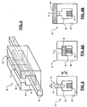
- FIG. 4 is a perspective view showing a power inductor with a slotted air gap arranged in the magnetic core material according to the present invention
- FIG. 5 is a cross sectional view of the power inductor of FIG. 4;
- FIGs. 6A and 6B are cross sectional views showing alternate embodiments with an eddy current reducing material that is arranged adjacent to the slotted air gap;
- FIG. 7 is a cross sectional view showing an alternate embodiment with additional space between the slotted air gap and a top of the conductor;
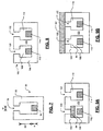
- FIG. 8 is a cross sectional view of a magnetic core with multiple cavities each with a slotted air gap
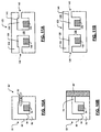
- FIGs. 9A and 9B are cross sectional views of FIG. 8 with an eddy current reducing material arranged adjacent to one or both of the slotted air gaps;
- FIG. 10A is a cross sectional view showing an alternate side location for the slotted air gap
- FIG. 10B is a cross sectional view showing an alternate side location for the slotted air gap
- FIGs. 11A and 11B are cross sectional views of a magnetic core with multiple cavities each with a side slotted air gap
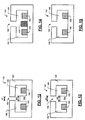
- FIG. 12 is a cross sectional view of a magnetic core with multiple cavities and a central slotted air gap
- FIG. 13 is a cross sectional view of a magnetic core with multiple cavities and a wider central slotted air gap
- FIG. 14 is a cross sectional view of a magnetic core with multiple cavities, a central slotted air gap and a material having a lower permability arranged between adjacent conductors;
- FIG. 15 is a cross sectional view of a magnetic core with multiple cavities and a central slotted air gap
- FIG. 16 is a cross sectional view of a magnetic core material with a slotted air gap and one or more insulated conductors
- FIG. 17 is a cross sectional view of a "C"-shaped magnetic core material and an eddy current reducing material
- FIG. 18 is a cross sectional view of a "C"-shaped magnetic core material and an eddy current reducing material with a mating projection;
- FIG. 19 is a cross sectional view of a "C"-shaped magnetic core material with multiple cavities and an eddy current reducing material.
- a power inductor 50 includes a conductor 54 that passes through a magnetic core material 58.
- the magnetic core material 58 may have a square outer cross-section 60 and a square central cavity 64 that extends the length of the magnetic core material.
- the conductor 54 may also have a square cross section. While the square outer cross section 60, the square central cavity 64, and the conductor 54 are shown, skilled artisans will appreciate that other shapes may be employed.
- the cross sections of the square outer cross section 60, the square central cavity 64, and the conductor 54 need not have the same shape.
- the conductor 54 passes through the central cavity 64 along one side of the cavity 64.
- the relatively high levels of DC current that flow through the conductor 30 tend to cause the magnetic core material 34 to saturate, which reduces performance of the power inductor and/or the device incorporating it.
- the magnetic core material 58 includes a slotted air gap 70 that runs lengthwise along the magnetic core material 58.
- the slotted air gap 70 runs in a direction that is parallel to the conductor 54.
- the slotted air gap 70 reduces the likelihood of saturation in the magnetic core material 58 for a given DC current level.
- magnetic flux 80-1 and 80-2 (collectively referred to as flux 80) is created by the slotted air gap 70.
- Magnetic flux 80-2 projects towards the conductor 54 and induces eddy currents in the conductor 54.
- a sufficient distance "D" is defined between the conductor 54 and a bottom of the slotted air gap 70 such that the magnetic flux is substantially reduced.
- the distance D is related to the current flowing through the conductor, a width "W" that is defined by the slotted air gap 70, and a desired maximum acceptable eddy current that can be induced in the conductor 54.
- a eddy current reducing material 84 can be arranged adjacent to the slotted air gap 70.
- the eddy current reducing material has a lower magnetic permeability than the magnetic core material and a higher permability than air. As a result, more magnetic flux flows through the material 84 than air.
- the magnetic insulating material 84 can be a soft magnetic material, a powdered metal, or any other suitable material.
- the eddy current reducing material 84 extends across a bottom opening of the slotted air gap 70.
- the eddy current reducing material 84' extends across an outer opening of the slotted air gap. Since the eddy current reducing material 84' has a lower magnetic permeability than the magnetic core material and a higher magnetic permeability than air, more flux flows through the eddy current reducing material than the air. Thus, less of the magnetic flux that is generated by the slotted air gap reaches the conductor.
- the eddy current reducing material 84 can have a relative permeability of 9 while air in the air gap has a relative permeability of 1. As a result, approximately 90% of the magnetic flux flows through the material 84 and approximately 10% of the magnetic flux flows through the air. As a result, the magnetic flux reaching the conductor is significantly reduced, which reduces induced eddy currents in the conductor. As can be appreciated, other materials having other permeability values can be used. Referring now to FIG. 7, a distance "D2" between a bottom the slotted air gap and a top of the conductor 54 can also be increased to reduce the magnitude of eddy currents that are induced in the conductor 54.
- a power inductor 100 includes a magnetic core material 104 that defines first and second cavities 108 and 110.
- First and second conductors 112 and 114 are arranged in the first and second cavities 108 and 110, respectively.
- First and second slotted air gaps 120 and 122 are arranged in the magnetic core material 104 on a side that is across from the conductors 112 and 114, respectively.
- the first and second slotted air gaps 120 and 122 reduce saturation of the magnetic core material 104.
- mutual coupling M is in the range of 0.5.
- an eddy current reducing material is arranged adjacent to one or more of the slotted air gaps 120 and/or 122 to reduce magnetic flux caused by the slotted air gaps, which reduces induced eddy currents.
- the eddy current reducing material 84 is located adjacent to a bottom opening of the slotted air gaps 120.
- the eddy current reducing material is located adjacent to a top opening of both of the slotted air gaps 120 and 122.
- the eddy current reducing material can be located adjacent to one or both of the slotted air gaps.
- "T"-shaped central section 123 of the magnetic core material separates the first and second cavities 108 and 110.
- the slotted air gap can be located in various other positions.
- a slotted air gap 70' can be arranged on one of the sides of the magnetic core material 58.
- a bottom edge of the slotted air gap 70' is preferably but not necessarily arranged above a top surface of the conductor 54.
- the magnetic flux radiates inwardly. Since the slotted air gap 70' is arranged above the conductor 54, the magnetic flux has a reduced impact.
- the eddy current reducing material can arranged adjacent to the slotted air gap 70' to further reduce the magnetic flux as shown in FIGs. 6A and/or 6B.
- the eddy current reducing material 84' is located adjacent to an outer opening of the slotted air gap 70'.
- the eddy current reducing material 84 can be located inside of the magnetic core material 58 as well.
- a power inductor 123 includes a magnetic core material 124 that defines first and second cavities 126 and 128, which are separated by a central portion 129.
- First and second conductors 130 and 132 are arranged in the first and second cavities 126 and 128, respectively, adjacent to one side.
- First and second slotted air gaps 138 and 140 are arranged in opposite sides of the magnetic core material adjacent to one side with the conductors 130 and 132.
- the slotted air gaps 138 and/or 140 can be aligned with an inner edge 141 of the magnetic core material 124 as shown in FIG. 11 B or spaced from the inner edge 141 as shown in FIG. 11A.
- the eddy current reducing material can be used to further reduce the magnetic flux emanating from one or both of the slotted air gaps as shown in FIGs. 6A and/or 6B.
- a power inductor 142 includes a magnetic core material 144 that defines first and second connected cavities 146 and 148.
- First and second conductors 150 and 152 are arranged in the first and second cavities 146 and 148, respectively.
- a projection 154 of the magnetic core material 144 extends upwardly from a bottom side of the magnetic core material between the conductors 150 and 152.
- the projection 154 extends partially but not fully towards to a top side.
- the projection 154 has a projection length that is greater than a height of the conductors 150 and 154.
- the projection 154 can also be made of a material having a lower permability than the magnetic core and a higher permability than air as shown at 155 in FIG. 14. Alternately, both the projection and the magnetic core material can be removed as shown in FIG. 15. In this embodiment, the mutual coupling M is approximately equal to 1.
- a slotted air gap 156 is arranged in the magnetic core material 144 in a location that is above the projection 154.
- the slotted air gap 156 has a width W1 that is less than a width W2 of the projection 154.
- a slotted air gap 156' is arranged in the magnetic core material in a location that is above the projection 154.
- the slotted air gap 156 has a width W3 that is greater than or equal to a width W2 of the projection 154.
- the eddy current reducing material can be used to further reduce the magnetic flux emanating from the slotted air gaps 156 and/or 156' as shown in FIGs. 6A and/or 6B.
- mutual coupling M is in the range of 1.
- a power inductor 170 includes a magnetic core material 172 that defines a cavity 174.
- a slotted air gap 175 is formed in one side of the magnetic core material 172.
- One or more insulated conductors 176 and 178 pass through the cavity 174.
- the insulated conductors 176 and 178 include an outer layer 182 surrounding an inner conductor 184.
- the outer layer 182 has a higher permability than air and lower than the magnetic core material. The outer material 182 significantly reduces the magnetic flux caused by the slotted air gap and reduces eddy currents that would otherwise be induced in the conductors 184.
- a power inductor 180 includes a conductor 184 and a "C"-shaped magnetic core material 188 that defines a cavity 190.
- a slotted air gap 192 is located on one side of the magnetic core material 188.
- the conductor 184 passes through the cavity 190.
- An eddy current reducing material 84' is located across the slotted air gap 192.
- the eddy current reducing material 84' includes a projection 194 that extends into the slotted air gap and that mates with the opening that is defined by the slotted air gap 192.
- the power inductor 200 a magnetic core material that defines first and second cavities 206 and 208.
- First and second conductors 210 and 212 pass through the first and second cavities 206 and 208, respectively.
- a center section 218 is located between the first and second cavities.
- the center section 218 may be made of the magnetic core material and/or an eddy current reducing material.
- the conductors may include an outer layer.
- the conductors may be made of copper, although gold, aluminum, and/or other suitable conducting materials having a low resistance may be used.
- the magnetic core material can be Ferrite although other magnetic core materials having a high magnetic permeability and a high electrical resistivity can be used.
- Ferrite refers to any of several magnetic substances that include ferric oxide combined with the oxides of one or more metals such as manganese, nickel, and/or zinc. If Ferrite is employed, the slotted air gap can be cut with a diamond cutting blade or other suitable technique.
- the power inductor in accordance with the present embodiments preferably has the capacity to handle up to 100 Amps (A) of DC current and has an inductance of 500 nH or less. For example, a typical inductance value of 50 nH is used. While the present invention has been illustrated in conjunction with DC/DC converters, skilled artisans will appreciate that the power inductor can be used in a wide variety of other applications.
Landscapes
- Engineering & Computer Science (AREA)
- Power Engineering (AREA)
- Chemical & Material Sciences (AREA)
- Composite Materials (AREA)
- Microelectronics & Electronic Packaging (AREA)
- Coils Or Transformers For Communication (AREA)
- Electric Propulsion And Braking For Vehicles (AREA)
Abstract
Description
- The present invention relates to inductors, and more particularly to power inductors having magnetic core materials with reduced levels of saturation when operating with high DC currents and at high operating frequencies.
- Inductors are circuit elements that operate based on magnetic fields. The source of the magnetic field is charge that is in motion, or current. If current varies with time, the magnetic field that is induced also varies with time. A time-varying magnetic field induces a voltage in any conductor that is linked by the magnetic field. If the current is constant, the voltage across an ideal inductor is zero. Therefore, the inductor looks like a short circuit to a constant or DC current. In the inductor, the voltage is given by:
- Inductors can be used in a wide variety of circuits. Power inductors receive a relatively high DC current, for example up to about 100 Amps, and may operate at relatively high frequencies. For example and referring now to FIG. 1, a
power inductor 20 may be used in a DC/DC converter 24, which typically employs inversion and/or rectification to transform DC at one voltage to DC at another voltage. - Referring now to FIG. 2, the
power inductor 20 typically includes one or more turns of aconductor 30 that pass through amagnetic core material 34. For example, themagnetic core material 34 may have a squareouter cross-section 36 and a squarecentral cavity 38 that extends the length of themagnetic core material 34. Theconductor 30 passes through thecentral cavity 38. The relatively high levels of DC current that flow through theconductor 30 tend to cause themagnetic core material 34 to saturate, which reduces the performance of thepower inductor 20 and the device incorporating it. - A power inductor includes a magnetic core material having first and second ends. An inner cavity arranged in the magnetic core material extends from the first end to the second end. A conductor passes through the cavity. A slotted air gap arranged in the magnetic core material extends from the first end to the second end.
- In other features, a system comprises the power inductor and further comprises a DC/DC converter that communicates with the power inductor.
- In other features, the slotted air gap is arranged in the magnetic core material in a direction that is parallel to the conductor. An eddy current reducing material is arranged adjacent to at least one of an inner opening of the slotted air gap in the cavity between the slotted air gap and the conductor and an outer opening of the slotted air gap. The eddy current reducing material has a permeability that is lower than the magnetic core material.
- In yet other features, the conductor passes through the cavity along a first side of the magnetic core material and the slotted air gap is arranged in a second side of the magnetic core material that is opposite the first side. The conductor passes through the cavity along a first side of the magnetic core material and the slotted air gap is arranged in a second side that is adjacent to the first side. A second conductor passes through the cavity along the first side. A projection of the magnetic core material extends outwardly from the first side between the conductor and the second conductor. The slotted air gap is arranged in the opposite side of the magnetic core material above the projection.
- In still other features, a second cavity is arranged in the magnetic core material. A center section of the magnetic core material is arranged between the cavity and the second cavity. A second conductor passes through the second cavity adjacent to the first side. A second slotted air gap is arranged in a third side that is opposite to the second side.
- In other features, a second cavity is arranged in the magnetic core material. A center "T"-shaped section is arranged in the magnetic core material between the cavity and the second cavity. A second conductor passes through the second cavity adjacent to the first side. The first conductor is arranged adjacent to the first side. The slotted air gap is arranged in a second side that is opposite the first side on one side of the center "T"-shaped section and a second slotted air gap is arranged in the second side that is opposite the first side on an opposite side of the center "T"-shaped section. The slotted air gap is arranged in a second side of the magnetic core material that is adjacent to the first side. A second slotted air gap is arranged in a third side that is opposite the second side.
- In other features, the eddy current reducing material has a low magnetic permeability. The eddy current reducing material comprises a soft magnetic material. The conductor includes an insulating material arranged on an outer surface thereof. The projection includes a material having a permeability lower than the magnetic core material. The soft magnetic material comprises a powdered material. A cross sectional shape of the magnetic core material is one of square, circular, rectangular, elliptical, and oval.
- Further areas of applicability of the present invention will become apparent from the detailed description provided hereinafter. It should be understood that the detailed description and specific examples, while indicating the preferred embodiment of the invention, are intended for purposes of illustration only and are not intended to limit the scope of the invention.
- The present invention will become more fully understood from the detailed description and the accompanying drawings, wherein:
- FIG. 1 is a functional block diagram and electrical schematic of a power inductor implemented in an exemplary DC/DC converter according to the prior art;
- FIG. 2 is a perspective view showing the power inductor of FIG. 1 according to the prior art;
- FIG. 3 is a cross sectional view showing the power inductor of FIGs. 1 and 2 according to the prior art;
- FIG. 4 is a perspective view showing a power inductor with a slotted air gap arranged in the magnetic core material according to the present invention;
- FIG. 5 is a cross sectional view of the power inductor of FIG. 4;
- FIGs. 6A and 6B are cross sectional views showing alternate embodiments with an eddy current reducing material that is arranged adjacent to the slotted air gap;
- FIG. 7 is a cross sectional view showing an alternate embodiment with additional space between the slotted air gap and a top of the conductor;
- FIG. 8 is a cross sectional view of a magnetic core with multiple cavities each with a slotted air gap;
- FIGs. 9A and 9B are cross sectional views of FIG. 8 with an eddy current reducing material arranged adjacent to one or both of the slotted air gaps;
- FIG. 10A is a cross sectional view showing an alternate side location for the slotted air gap;
- FIG. 10B is a cross sectional view showing an alternate side location for the slotted air gap;
- FIGs. 11A and 11B are cross sectional views of a magnetic core with multiple cavities each with a side slotted air gap;
- FIG. 12 is a cross sectional view of a magnetic core with multiple cavities and a central slotted air gap;
- FIG. 13 is a cross sectional view of a magnetic core with multiple cavities and a wider central slotted air gap;
- FIG. 14 is a cross sectional view of a magnetic core with multiple cavities, a central slotted air gap and a material having a lower permability arranged between adjacent conductors;
- FIG. 15 is a cross sectional view of a magnetic core with multiple cavities and a central slotted air gap;
- FIG. 16 is a cross sectional view of a magnetic core material with a slotted air gap and one or more insulated conductors;
- FIG. 17 is a cross sectional view of a "C"-shaped magnetic core material and an eddy current reducing material;
- FIG. 18 is a cross sectional view of a "C"-shaped magnetic core material and an eddy current reducing material with a mating projection; and
- FIG. 19 is a cross sectional view of a "C"-shaped magnetic core material with multiple cavities and an eddy current reducing material.
- The following description of the preferred embodiment(s) is merely exemplary in nature and is in no way intended to limit the invention, its application, or uses. For purposes of clarity, the same reference numbers will be used in the drawings to identify the same elements.
- Referring now to FIG. 4, a
power inductor 50 includes aconductor 54 that passes through amagnetic core material 58. For example, themagnetic core material 58 may have a squareouter cross-section 60 and a squarecentral cavity 64 that extends the length of the magnetic core material. Theconductor 54 may also have a square cross section. While the squareouter cross section 60, the squarecentral cavity 64, and theconductor 54 are shown, skilled artisans will appreciate that other shapes may be employed. The cross sections of the squareouter cross section 60, the squarecentral cavity 64, and theconductor 54 need not have the same shape. Theconductor 54 passes through thecentral cavity 64 along one side of thecavity 64. The relatively high levels of DC current that flow through theconductor 30 tend to cause themagnetic core material 34 to saturate, which reduces performance of the power inductor and/or the device incorporating it. - According to the present invention, the
magnetic core material 58 includes a slottedair gap 70 that runs lengthwise along themagnetic core material 58. The slottedair gap 70 runs in a direction that is parallel to theconductor 54. The slottedair gap 70 reduces the likelihood of saturation in themagnetic core material 58 for a given DC current level. - Referring now to FIG. 5, magnetic flux 80-1 and 80-2 (collectively referred to as flux 80) is created by the slotted
air gap 70. Magnetic flux 80-2 projects towards theconductor 54 and induces eddy currents in theconductor 54. In a preferred embodiment, a sufficient distance "D" is defined between theconductor 54 and a bottom of the slottedair gap 70 such that the magnetic flux is substantially reduced. In one exemplary embodiment, the distance D is related to the current flowing through the conductor, a width "W" that is defined by the slottedair gap 70, and a desired maximum acceptable eddy current that can be induced in theconductor 54. - Referring now to FIGs. 6A and 6B, a eddy
current reducing material 84 can be arranged adjacent to the slottedair gap 70. The eddy current reducing material has a lower magnetic permeability than the magnetic core material and a higher permability than air. As a result, more magnetic flux flows through the material 84 than air. For example, the magnetic insulatingmaterial 84 can be a soft magnetic material, a powdered metal, or any other suitable material. In FIG. 6A, the eddycurrent reducing material 84 extends across a bottom opening of the slottedair gap 70. - In FIG. 6B, the eddy current reducing material 84' extends across an outer opening of the slotted air gap. Since the eddy current reducing material 84' has a lower magnetic permeability than the magnetic core material and a higher magnetic permeability than air, more flux flows through the eddy current reducing material than the air. Thus, less of the magnetic flux that is generated by the slotted air gap reaches the conductor.
- For example, the eddy
current reducing material 84 can have a relative permeability of 9 while air in the air gap has a relative permeability of 1. As a result, approximately 90% of the magnetic flux flows through thematerial 84 and approximately 10% of the magnetic flux flows through the air. As a result, the magnetic flux reaching the conductor is significantly reduced, which reduces induced eddy currents in the conductor. As can be appreciated, other materials having other permeability values can be used. Referring now to FIG. 7, a distance "D2" between a bottom the slotted air gap and a top of theconductor 54 can also be increased to reduce the magnitude of eddy currents that are induced in theconductor 54. - Referring now to FIG. 8, a
power inductor 100 includes amagnetic core material 104 that defines first andsecond cavities second conductors second cavities air gaps magnetic core material 104 on a side that is across from theconductors air gaps magnetic core material 104. In one embodiment, mutual coupling M is in the range of 0.5. - Referring now to FIGs. 9A and 9B, an eddy current reducing material is arranged adjacent to one or more of the slotted
air gaps 120 and/or 122 to reduce magnetic flux caused by the slotted air gaps, which reduces induced eddy currents. In FIG. 9A, the eddycurrent reducing material 84 is located adjacent to a bottom opening of the slottedair gaps 120. In FIG. 9B, the eddy current reducing material is located adjacent to a top opening of both of the slottedair gaps central section 123 of the magnetic core material separates the first andsecond cavities - The slotted air gap can be located in various other positions. For example and referring now to FIG. 10A, a slotted air gap 70' can be arranged on one of the sides of the
magnetic core material 58. A bottom edge of the slotted air gap 70' is preferably but not necessarily arranged above a top surface of theconductor 54. As-can be seen, the magnetic flux radiates inwardly. Since the slotted air gap 70' is arranged above theconductor 54, the magnetic flux has a reduced impact. As can be appreciated, the eddy current reducing material can arranged adjacent to the slotted air gap 70' to further reduce the magnetic flux as shown in FIGs. 6A and/or 6B. In FIG. 10B, the eddy current reducing material 84' is located adjacent to an outer opening of the slotted air gap 70'. The eddycurrent reducing material 84 can be located inside of themagnetic core material 58 as well. - Referring now to FIGs. 11 A and 11B, a
power inductor 123 includes amagnetic core material 124 that defines first andsecond cavities central portion 129. First andsecond conductors second cavities air gaps conductors air gaps 138 and/or 140 can be aligned with aninner edge 141 of themagnetic core material 124 as shown in FIG. 11 B or spaced from theinner edge 141 as shown in FIG. 11A. As can be appreciated, the eddy current reducing material can be used to further reduce the magnetic flux emanating from one or both of the slotted air gaps as shown in FIGs. 6A and/or 6B. - Referring now to FIGs. 12 and 13, a
power inductor 142 includes amagnetic core material 144 that defines first and secondconnected cavities second conductors second cavities projection 154 of themagnetic core material 144 extends upwardly from a bottom side of the magnetic core material between theconductors projection 154 extends partially but not fully towards to a top side. In a preferred embodiment, theprojection 154 has a projection length that is greater than a height of theconductors projection 154 can also be made of a material having a lower permability than the magnetic core and a higher permability than air as shown at 155 in FIG. 14. Alternately, both the projection and the magnetic core material can be removed as shown in FIG. 15. In this embodiment, the mutual coupling M is approximately equal to 1. - In FIG. 12, a slotted
air gap 156 is arranged in themagnetic core material 144 in a location that is above theprojection 154. The slottedair gap 156 has a width W1 that is less than a width W2 of theprojection 154. In FIG. 13, a slotted air gap 156' is arranged in the magnetic core material in a location that is above theprojection 154. The slottedair gap 156 has a width W3 that is greater than or equal to a width W2 of theprojection 154. As can be appreciated, the eddy current reducing material can be used to further reduce the magnetic flux emanating from the slottedair gaps 156 and/or 156' as shown in FIGs. 6A and/or 6B. In some implementations of FIGs. 12-14, mutual coupling M is in the range of 1. - Referring now to FIG. 16, a
power inductor 170 is shown and includes amagnetic core material 172 that defines acavity 174. A slottedair gap 175 is formed in one side of themagnetic core material 172. One or moreinsulated conductors 176 and 178 pass through thecavity 174. Theinsulated conductors 176 and 178 include anouter layer 182 surrounding aninner conductor 184. Theouter layer 182 has a higher permability than air and lower than the magnetic core material. Theouter material 182 significantly reduces the magnetic flux caused by the slotted air gap and reduces eddy currents that would otherwise be induced in theconductors 184. - Referring now to FIG. 17, a
power inductor 180 includes aconductor 184 and a "C"-shapedmagnetic core material 188 that defines acavity 190. A slottedair gap 192 is located on one side of themagnetic core material 188. Theconductor 184 passes through thecavity 190. An eddy current reducing material 84' is located across the slottedair gap 192. In FIG. 18, the eddy current reducing material 84' includes aprojection 194 that extends into the slotted air gap and that mates with the opening that is defined by the slottedair gap 192. - Referring now to FIG. 19, the power inductor 200 a magnetic core material that defines first and
second cavities second conductors second cavities center section 218 is located between the first and second cavities. As can be appreciated, thecenter section 218 may be made of the magnetic core material and/or an eddy current reducing material. Alternately, the conductors may include an outer layer. - The conductors may be made of copper, although gold, aluminum, and/or other suitable conducting materials having a low resistance may be used. The magnetic core material can be Ferrite although other magnetic core materials having a high magnetic permeability and a high electrical resistivity can be used. As used herein, Ferrite refers to any of several magnetic substances that include ferric oxide combined with the oxides of one or more metals such as manganese, nickel, and/or zinc. If Ferrite is employed, the slotted air gap can be cut with a diamond cutting blade or other suitable technique.
- While some of the power inductors that are shown have one turn, skilled artisans will appreciate that additional turns may be employed. While some of the embodiments only show a magnetic core material with one or two cavities each with one or two conductors, additional conductors may be employed in each cavity and/or additional cavities and conductors may be employed without departing from the invention. While the shape of the cross section of the inductor has be shown as square, other suitable shapes, such as rectangular, circular, oval, elliptical and the like are also contemplated.
- The power inductor in accordance with the present embodiments preferably has the capacity to handle up to 100 Amps (A) of DC current and has an inductance of 500 nH or less. For example, a typical inductance value of 50 nH is used. While the present invention has been illustrated in conjunction with DC/DC converters, skilled artisans will appreciate that the power inductor can be used in a wide variety of other applications.
- Those skilled in the art can now appreciate from the foregoing description that the broad teachings of the present invention can be implemented in a variety of forms. Therefore, while this invention has been described in connection with particular examples thereof, the true scope of the invention should not be so limited since other modifications will become apparent to the skilled practitioner upon a study of the drawings, the specification and the following claims.
Claims (21)
- A power inductor comprising:a magnetic core material having first and second ends;an inner cavity arranged in said magnetic core material that extends from said first end to said second end;a conductor that passes through said cavity; anda slotted air gap arranged in said magnetic core material that extends from said first end to said second end.
- A system comprising the power inductor of claim 1 and further comprising a DC/DC converter that communicates with said power inductor.
- The power inductor of claim 1 wherein said slotted air gap is arranged in said magnetic core material in a direction that is parallel to said conductor.
- The power inductor of claim 1 further comprising an eddy current reducing material that is arranged adjacent to at least one of an inner opening of said slotted air gap in said cavity between said slotted air gap and said conductor and an outer opening of said slotted air gap, wherein said eddy current reducing material has a permeability that is lower than said magnetic core material.
- The power inductor of claim 1 wherein said conductor passes through said cavity along a first side of said magnetic core material and said slotted air gap is arranged in a second side of said magnetic core material that is opposite said first side.
- The power inductor of claim 1 wherein said conductor passes through said cavity along a first side of said magnetic core material and said slotted air gap is arranged in a second side that is adjacent to said first side.
- The power inductor of claim 5 wherein a second conductor passes through said cavity along said first side.
- The power inductor of claim 7 further comprising a projection of said magnetic core material that extends outwardly from said first side between said conductor and said second conductor.
- The power inductor of claim 8 wherein said slotted air gap is arranged in said opposite side of said magnetic core material above said projection.
- The power inductor of claim 6 further comprising:a second cavity arranged in said magnetic core material;a center section of said magnetic core material that is arranged between said cavity and said second cavity;a second conductor that passes through said second cavity adjacent to said first side; anda second slotted air gap arranged in a third side that is opposite to said second side.
- The power inductor of claim 1 further comprising:a second cavity in said magnetic core material;a center "T"-shaped section arranged in said magnetic core material between said cavity and said second cavity; anda second conductor that passes through said second cavity adjacent to said first side, wherein said first conductor is arranged adjacent to said first side.
- The power inductor of claim 11 wherein said slotted air gap is arranged in a second side that is opposite said first side on one side of said center "T"-shaped section and a second slotted air gap is arranged in said second side that is opposite said first side on an opposite side of said center "T"-shaped section.
- The power inductor of claim 11 wherein said slotted air gap is arranged in a second side of said magnetic core material that is adjacent to said first side and wherein a second slotted air gap is arranged in a third side that is opposite said second side.
- The power inductor of claim 4 wherein said eddy current reducing material has a low magnetic permeability.
- The power inductor of Claim 14 wherein said eddy current reducing material comprises a soft magnetic material.
- The power inductor of Claim 4 wherein said conductor includes an insulating material arranged on an outer surface thereof.
- The power inductor of Claim 8 wherein said projection includes a material having a permeability lower than said magnetic core material.
- The power inductor of Claim 17 wherein said material comprises a soft magnetic material.
- The power inductor of claim 1 wherein a cross sectional shape of said magnetic core material is one of square, circular, rectangular, elliptical, and oval.
- The power inductor of claim 15 wherein the soft magnetic material comprises a powdered metal.
- The power inductor of claim 18 wherein the soft magnetic material comprises a powdered metal.
Applications Claiming Priority (2)
| Application Number | Priority Date | Filing Date | Title |
|---|---|---|---|
| US621128 | 1990-11-30 | ||
| US10/621,128 US7023313B2 (en) | 2003-07-16 | 2003-07-16 | Power inductor with reduced DC current saturation |
Publications (2)
| Publication Number | Publication Date |
|---|---|
| EP1498914A1 true EP1498914A1 (en) | 2005-01-19 |
| EP1498914B1 EP1498914B1 (en) | 2016-09-07 |
Family
ID=33477110
Family Applications (1)
| Application Number | Title | Priority Date | Filing Date |
|---|---|---|---|
| EP04010841.7A Expired - Lifetime EP1498914B1 (en) | 2003-07-16 | 2004-05-06 | Power inductor with reduced DC current saturation |
Country Status (5)
| Country | Link |
|---|---|
| US (2) | US7023313B2 (en) |
| EP (1) | EP1498914B1 (en) |
| JP (1) | JP4473040B2 (en) |
| CN (1) | CN100555482C (en) |
| TW (1) | TWI333219B (en) |
Families Citing this family (27)
| Publication number | Priority date | Publication date | Assignee | Title |
|---|---|---|---|---|
| US7190152B2 (en) * | 2004-07-13 | 2007-03-13 | Marvell World Trade Ltd. | Closed-loop digital control system for a DC/DC converter |
| JP2006120887A (en) * | 2004-10-22 | 2006-05-11 | Sumida Corporation | Magnetic element |
| JP4626389B2 (en) * | 2005-05-13 | 2011-02-09 | 富士電機システムズ株式会社 | Combined reactor |
| US7864015B2 (en) * | 2006-04-26 | 2011-01-04 | Vishay Dale Electronics, Inc. | Flux channeled, high current inductor |
| US8018310B2 (en) * | 2006-09-27 | 2011-09-13 | Vishay Dale Electronics, Inc. | Inductor with thermally stable resistance |
| JP4685128B2 (en) * | 2007-06-08 | 2011-05-18 | Necトーキン株式会社 | Inductor |
| US7948346B2 (en) * | 2008-06-30 | 2011-05-24 | Alpha & Omega Semiconductor, Ltd | Planar grooved power inductor structure and method |
| JP5375922B2 (en) * | 2011-10-18 | 2013-12-25 | 株式会社豊田自動織機 | Magnetic core and induction device |
| JP5494612B2 (en) | 2011-10-18 | 2014-05-21 | 株式会社豊田自動織機 | Magnetic core and induction device |
| US9389619B2 (en) | 2013-07-29 | 2016-07-12 | The Boeing Company | Transformer core flux control for power management |
| US9455084B2 (en) | 2012-07-19 | 2016-09-27 | The Boeing Company | Variable core electromagnetic device |
| US9159487B2 (en) * | 2012-07-19 | 2015-10-13 | The Boeing Company | Linear electromagnetic device |
| US9947450B1 (en) | 2012-07-19 | 2018-04-17 | The Boeing Company | Magnetic core signal modulation |
| US9568563B2 (en) | 2012-07-19 | 2017-02-14 | The Boeing Company | Magnetic core flux sensor |
| US10840005B2 (en) | 2013-01-25 | 2020-11-17 | Vishay Dale Electronics, Llc | Low profile high current composite transformer |
| US9651633B2 (en) | 2013-02-21 | 2017-05-16 | The Boeing Company | Magnetic core flux sensor |
| JP2016025273A (en) * | 2014-07-23 | 2016-02-08 | Fdk株式会社 | Winding parts |
| CN105869853B (en) | 2015-01-23 | 2018-09-04 | 台达电子工业股份有限公司 | Magnetic core element and transformer |
| KR20160094754A (en) * | 2015-02-02 | 2016-08-10 | 삼성전자주식회사 | Display apparatus and control methods thereof |
| US10102962B1 (en) * | 2015-09-22 | 2018-10-16 | Apple Inc. | Integrated magnetic passive devices using magnetic film |
| US10403429B2 (en) | 2016-01-13 | 2019-09-03 | The Boeing Company | Multi-pulse electromagnetic device including a linear magnetic core configuration |
| US10998124B2 (en) | 2016-05-06 | 2021-05-04 | Vishay Dale Electronics, Llc | Nested flat wound coils forming windings for transformers and inductors |
| KR102571361B1 (en) | 2016-08-31 | 2023-08-25 | 비쉐이 데일 일렉트로닉스, 엘엘씨 | Inductor having high current coil with low direct current resistance |
| US12567533B2 (en) | 2020-03-03 | 2026-03-03 | Vishay Dale Electronics, Llc | Inductor with preformed termination and method and assembly for making the same |
| CN112151238B (en) * | 2020-08-27 | 2025-07-08 | 合肥矽力杰半导体技术有限公司 | Transformer |
| USD1034462S1 (en) | 2021-03-01 | 2024-07-09 | Vishay Dale Electronics, Llc | Inductor package |
| US11948724B2 (en) | 2021-06-18 | 2024-04-02 | Vishay Dale Electronics, Llc | Method for making a multi-thickness electro-magnetic device |
Citations (5)
| Publication number | Priority date | Publication date | Assignee | Title |
|---|---|---|---|---|
| DE3622190A1 (en) * | 1986-03-14 | 1988-01-07 | Philips Patentverwaltung | Coil Core |
| EP0484074A2 (en) * | 1990-10-29 | 1992-05-06 | General Electric Company | High-frequency, high-leakage-reactance transformer |
| GB2318691A (en) * | 1996-10-28 | 1998-04-29 | Norweb Plc | Inductor arrangement and a method for its manufacture |
| EP0895257A1 (en) * | 1997-07-29 | 1999-02-03 | Murata Manufacturing Co., Ltd. | Noise-suppressing component |
| WO2002095775A1 (en) * | 2001-05-21 | 2002-11-28 | Milli Sensor Systems & Actuators, Inc. | Planar miniature inductors and transformers and miniature transformers for millimachined instruments |
Family Cites Families (123)
| Publication number | Priority date | Publication date | Assignee | Title |
|---|---|---|---|---|
| US3146300A (en) | 1959-09-18 | 1964-08-25 | Asea Ab | Corona protection screen for inductor coils in vacuum furnaces |
| US3305697A (en) | 1963-11-12 | 1967-02-21 | Gen Electric | Ballast apparatus with air-core inductor |
| US3579214A (en) | 1968-06-17 | 1971-05-18 | Ibm | Multichannel magnetic head with common leg |
| US3599325A (en) | 1969-06-09 | 1971-08-17 | Photocircuits Corp | Method of making laminated wire wound armatures |
| US3851375A (en) | 1972-05-08 | 1974-12-03 | Philips Corp | Method of bonding together mouldings of sintered oxidic ferromagnetic material |
| US3766308A (en) | 1972-05-25 | 1973-10-16 | Microsystems Int Ltd | Joining conductive elements on microelectronic devices |
| US4031496A (en) | 1973-07-06 | 1977-06-21 | Hitachi, Ltd. | Variable inductor |
| US4020439A (en) | 1974-02-09 | 1977-04-26 | U.S. Philips Corporation | Inductive stabilizing ballast for a gas and/or vapor discharge lamp |
| JPS5217808A (en) | 1975-07-31 | 1977-02-10 | Olympus Optical Co Ltd | Manufacturing method of magnetic head |
| US4047138A (en) | 1976-05-19 | 1977-09-06 | General Electric Company | Power inductor and transformer with low acoustic noise air gap |
| GB1542320A (en) * | 1976-10-26 | 1979-03-14 | Labofina Sa | Process for the preparation of aromatic dicarboxylic acids |
| DE2714426C3 (en) | 1977-03-31 | 1981-02-26 | Siemens Ag, 1000 Berlin Und 8000 Muenchen | Passive circuit element designed as a low-pass element or as a delay element |
| US4116519A (en) | 1977-08-02 | 1978-09-26 | Amp Incorporated | Electrical connections for chip carriers |
| NL7900244A (en) | 1979-01-12 | 1980-07-15 | Philips Nv | FLAT TWO-LAYER ELECTRICAL COIL. |
| US4371912A (en) | 1980-10-01 | 1983-02-01 | Motorola, Inc. | Method of mounting interrelated components |
| JPS57193007A (en) | 1981-10-23 | 1982-11-27 | Tdk Corp | Magnetic core |
| DE3220737A1 (en) * | 1982-06-02 | 1983-12-08 | Siemens AG, 1000 Berlin und 8000 München | COLUMN-LOW RADIO EMISSION CONTROL |
| JPS58224420A (en) * | 1982-06-23 | 1983-12-26 | Matsushita Electric Ind Co Ltd | Magnetic head and its production |
| US4536733A (en) * | 1982-09-30 | 1985-08-20 | Sperry Corporation | High frequency inverter transformer for power supplies |
| US4527032A (en) * | 1982-11-08 | 1985-07-02 | Armco Inc. | Radio frequency induction heating device |
| US4475143A (en) | 1983-01-10 | 1984-10-02 | Rogers Corporation | Decoupling capacitor and method of manufacture thereof |
| FR2560429B1 (en) | 1984-02-28 | 1987-06-19 | Telemecanique Electrique | QUIET ELECTRO-MAGNET AND CONTACTOR USING SUCH ELECTRO-MAGNET |
| US4583068A (en) | 1984-08-13 | 1986-04-15 | At&T Bell Laboratories | Low profile magnetic structure in which one winding acts as support for second winding |
| JPS6178111A (en) | 1984-09-25 | 1986-04-21 | Matsushita Electric Works Ltd | Manufacture of magnetic core |
| JPH0424649Y2 (en) | 1985-02-18 | 1992-06-11 | ||
| US4616205A (en) | 1985-03-08 | 1986-10-07 | At&T Bell Laboratories | Preformed multiple turn transformer winding |
| US4641112A (en) | 1985-03-12 | 1987-02-03 | Toko, Inc. | Delay line device and method of making same |
| US4630170A (en) | 1985-03-13 | 1986-12-16 | Rogers Corporation | Decoupling capacitor and method of manufacture thereof |
| US4801912A (en) | 1985-06-07 | 1989-01-31 | American Precision Industries Inc. | Surface mountable electronic device |
| US4803609A (en) | 1985-10-31 | 1989-02-07 | International Business Machines Corporation | D. C. to D. C. converter |
| JPS636712U (en) * | 1986-06-30 | 1988-01-18 | ||
| US4728810A (en) | 1987-02-19 | 1988-03-01 | Westinghouse Electric Corp. | Electromagnetic contactor with discriminator for determining when an input control signal is true or false and method |
| FR2620852A1 (en) | 1987-09-17 | 1989-03-24 | Equip Electr Moteur | Magnetic circuit especially for ignition coil for internal combustion engine |
| US5050969A (en) * | 1988-12-26 | 1991-09-24 | Mitsubishi Mining And Cement Company Ltd. | Photo-driven switching apparatus |
| EP0379176B1 (en) | 1989-01-19 | 1995-03-15 | Burndy Corporation | Card edge connector |
| JPH02251107A (en) | 1989-03-24 | 1990-10-08 | Murata Mfg Co Ltd | Choke coil |
| GB2237400B (en) * | 1989-10-27 | 1994-04-20 | Eev Ltd | Control of liquid crystal display visual properties |
| JPH0425036A (en) | 1990-05-16 | 1992-01-28 | Mitsubishi Electric Corp | Microwave semiconductor device |
| US5834591A (en) | 1991-01-31 | 1998-11-10 | Washington University | Polypeptides and antibodies useful for the diagnosis and treatment of pathogenic neisseria and other microorganisms having type 4 pilin |
| US5187428A (en) | 1991-02-26 | 1993-02-16 | Miller Electric Mfg. Co. | Shunt coil controlled transformer |
| US5764500A (en) | 1991-05-28 | 1998-06-09 | Northrop Grumman Corporation | Switching power supply |
| US5175525A (en) | 1991-06-11 | 1992-12-29 | Astec International, Ltd. | Low profile transformer |
| US5359313A (en) | 1991-12-10 | 1994-10-25 | Toko, Inc. | Step-up transformer |
| US5225971A (en) | 1992-01-08 | 1993-07-06 | International Business Machines Corporation | Three coil bridge transformer |
| NL9200119A (en) | 1992-01-22 | 1993-08-16 | Du Pont Nederland | CONNECTOR WITH PLATE-SHAPED INTERNAL SHIELD. |
| US5303115A (en) | 1992-01-27 | 1994-04-12 | Raychem Corporation | PTC circuit protection device comprising mechanical stress riser |
| US5343616B1 (en) | 1992-02-14 | 1998-12-29 | Rock Ltd | Method of making high density self-aligning conductive networks and contact clusters |
| US5186647A (en) | 1992-02-24 | 1993-02-16 | At&T Bell Laboratories | High frequency electrical connector |
| US5204809A (en) * | 1992-04-03 | 1993-04-20 | International Business Machines Corporation | H-driver DC-to-DC converter utilizing mutual inductance |
| JPH0653394A (en) | 1992-07-28 | 1994-02-25 | Shinko Electric Ind Co Ltd | Plain support for multilayer leadframe |
| KR940008066A (en) | 1992-09-18 | 1994-04-28 | 윌리엄 이. 힐러 | Multilayer Lead Frame Assembly and Method for Integrated Circuits |
| US5509691A (en) | 1992-10-26 | 1996-04-23 | Gao Gesellschaft Fur Automation Und Organisation Mbh | Security element in the form of threads or strips to be embedded in security documents and a method for producing and testing the same |
| US5444600A (en) | 1992-12-03 | 1995-08-22 | Linear Technology Corporation | Lead frame capacitor and capacitively-coupled isolator circuit using the same |
| JPH06260869A (en) | 1993-03-04 | 1994-09-16 | Nippon Telegr & Teleph Corp <Ntt> | Noise filter |
| US5400006A (en) | 1993-04-23 | 1995-03-21 | Schlumberger Industries | Current transformer with plural part core |
| US5362257A (en) | 1993-07-08 | 1994-11-08 | The Whitaker Corporation | Communications connector terminal arrays having noise cancelling capabilities |
| US5500629A (en) | 1993-09-10 | 1996-03-19 | Meyer Dennis R | Noise suppressor |
| US5403196A (en) | 1993-11-09 | 1995-04-04 | Berg Technology | Connector assembly |
| US5399106A (en) | 1994-01-21 | 1995-03-21 | The Whitaker Corporation | High performance electrical connector |
| US5684445A (en) | 1994-02-25 | 1997-11-04 | Fuji Electric Co., Ltd. | Power transformer |
| US5481238A (en) | 1994-04-19 | 1996-01-02 | Argus Technologies Ltd. | Compound inductors for use in switching regulators |
| US5554050A (en) | 1995-03-09 | 1996-09-10 | The Whitaker Corporation | Filtering insert for electrical connectors |
| US5586914A (en) | 1995-05-19 | 1996-12-24 | The Whitaker Corporation | Electrical connector and an associated method for compensating for crosstalk between a plurality of conductors |
| JP3599205B2 (en) | 1995-09-12 | 2004-12-08 | Tdk株式会社 | Inductor element for noise suppression |
| WO1997006660A2 (en) | 1995-08-15 | 1997-02-27 | Bourns, Multifuse (Hong Kong), Ltd. | Surface mount conductive polymer devices and method for manufacturing such devices |
| US6520308B1 (en) | 1996-06-28 | 2003-02-18 | Coinstar, Inc. | Coin discrimination apparatus and method |
| US5781093A (en) | 1996-08-05 | 1998-07-14 | International Power Devices, Inc. | Planar transformer |
| US5808537A (en) | 1996-09-16 | 1998-09-15 | Kabushiki Kaisha Toyoda Jidoshokki Seisakusho | Inductor core for transferring electric power to a conveyor carriage |
| US6054764A (en) | 1996-12-20 | 2000-04-25 | Texas Instruments Incorporated | Integrated circuit with tightly coupled passive components |
| JPH10240436A (en) | 1996-12-26 | 1998-09-11 | Nikon Corp | Information processing device and recording medium |
| US5889373A (en) | 1996-12-30 | 1999-03-30 | General Electric Company | Fluorescent lamp ballast with current feedback using a dual-function magnetic device |
| US6018468A (en) | 1997-04-08 | 2000-01-25 | Eos Corporation | Multi-resonant DC-to-DC converter |
| JPH10303352A (en) | 1997-04-22 | 1998-11-13 | Toshiba Corp | Semiconductor device and method of manufacturing semiconductor device |
| US6144269A (en) | 1997-06-10 | 2000-11-07 | Fuji Electric Co., Ltd. | Noise-cut LC filter for power converter with overlapping aligned coil patterns |
| JP3302620B2 (en) | 1997-06-18 | 2002-07-15 | タケチ工業ゴム株式会社 | Noise absorber |
| US6512437B2 (en) * | 1997-07-03 | 2003-01-28 | The Furukawa Electric Co., Ltd. | Isolation transformer |
| JPH1174125A (en) | 1997-08-29 | 1999-03-16 | Fuji Elelctrochem Co Ltd | Bead inductor |
| JP3937265B2 (en) | 1997-09-29 | 2007-06-27 | エルピーダメモリ株式会社 | Semiconductor device |
| EP1023736B1 (en) * | 1997-10-14 | 2002-05-29 | Vacuumschmelze GmbH | Radio interference suppression choke |
| JP3618534B2 (en) | 1997-11-28 | 2005-02-09 | 同和鉱業株式会社 | Optical communication lamp device and manufacturing method thereof |
| US6049264A (en) | 1997-12-09 | 2000-04-11 | Siemens Automotive Corporation | Electromagnetic actuator with composite core assembly |
| US6114932A (en) | 1997-12-12 | 2000-09-05 | Telefonaktiebolaget Lm Ericsson | Inductive component and inductive component assembly |
| US5909037A (en) | 1998-01-12 | 1999-06-01 | Hewlett-Packard Company | Bi-level injection molded leadframe |
| JPH11204354A (en) | 1998-01-17 | 1999-07-30 | Kobe:Kk | Noise interruption transformer |
| TW403917B (en) | 1998-05-08 | 2000-09-01 | Koninkl Philips Electronics Nv | Inductive element |
| JP4020177B2 (en) * | 1998-05-21 | 2007-12-12 | 三菱電機株式会社 | Transformer |
| US6201186B1 (en) | 1998-06-29 | 2001-03-13 | Motorola, Inc. | Electronic component assembly and method of making the same |
| RU2190284C2 (en) | 1998-07-07 | 2002-09-27 | Закрытое акционерное общество "Техно-ТМ" | Two-sided electronic device |
| US6046662A (en) | 1998-09-29 | 2000-04-04 | Compaq Computer Corporation | Low profile surface mount transformer |
| US6612890B1 (en) | 1998-10-15 | 2003-09-02 | Handy & Harman (Ny Corp.) | Method and system for manufacturing electronic packaging units |
| US6087195A (en) | 1998-10-15 | 2000-07-11 | Handy & Harman | Method and system for manufacturing lamp tiles |
| TR199902411A3 (en) | 1998-11-02 | 2000-06-21 | Lincoln Global, Inc. | Output coil and method of use for direct current welding machine |
| JP2000236189A (en) | 1999-02-16 | 2000-08-29 | Minebea Co Ltd | Shielding device for electronic circuit for aircraft |
| US6683522B2 (en) | 1999-02-24 | 2004-01-27 | Milli Sensor Systems & Actuators, Inc. | Planar miniature inductors and transformers |
| JP3680627B2 (en) | 1999-04-27 | 2005-08-10 | 富士電機機器制御株式会社 | Noise filter |
| JP3913933B2 (en) | 1999-05-24 | 2007-05-09 | 三菱電機株式会社 | Rotor of rotating electric machine and method of magnetizing the magnetic body |
| AR024092A1 (en) | 1999-05-26 | 2002-09-04 | Abb Ab | INDUCTION DEVICES WITH DISTRIBUTED BURIALS |
| JP3366916B2 (en) * | 1999-06-03 | 2003-01-14 | スミダコーポレーション株式会社 | Inductance element |
| JP3804747B2 (en) | 1999-08-24 | 2006-08-02 | ローム株式会社 | Manufacturing method of semiconductor device |
| CA2282636A1 (en) | 1999-09-16 | 2001-03-16 | Philippe Viarouge | Power transformers and power inductors for low frequency applications using isotropic composite magnetic materials with high power to weight ratio |
| KR100339563B1 (en) | 1999-10-08 | 2002-06-03 | 구자홍 | Electronic parts attachment structure and its mathod |
| US6459349B1 (en) * | 2000-03-06 | 2002-10-01 | General Electric Company | Circuit breaker comprising a current transformer with a partial air gap |
| US6831377B2 (en) | 2000-05-03 | 2004-12-14 | University Of Southern California | Repetitive power pulse generator with fast rising pulse |
| JP3610884B2 (en) | 2000-06-02 | 2005-01-19 | 株式会社村田製作所 | Trance |
| JP3821355B2 (en) | 2000-08-09 | 2006-09-13 | Necトーキン株式会社 | Choke coil and manufacturing method thereof |
| JP2002057039A (en) | 2000-08-11 | 2002-02-22 | Hitachi Ferrite Electronics Ltd | Composite magnetic core |
| JP3551135B2 (en) | 2000-08-24 | 2004-08-04 | 松下電器産業株式会社 | Thin transformer and method of manufacturing the same |
| AU2001293299A1 (en) | 2000-09-20 | 2002-04-02 | Ascom Energy Systems Ag, Berne | Planar inductive element |
| US6820321B2 (en) | 2000-09-22 | 2004-11-23 | M-Flex Multi-Fineline Electronix, Inc. | Method of making electronic transformer/inductor devices |
| IL138834A0 (en) | 2000-10-03 | 2001-10-31 | Payton Planar Magnetics Ltd | A magnetically biased inductor or flyback transformer |
| US6693430B2 (en) | 2000-12-15 | 2004-02-17 | Schlumberger Technology Corporation | Passive, active and semi-active cancellation of borehole effects for well logging |
| US20020157117A1 (en) | 2001-03-06 | 2002-10-24 | Jacob Geil | Method and apparatus for video insertion loss equalization |
| US6362986B1 (en) * | 2001-03-22 | 2002-03-26 | Volterra, Inc. | Voltage converter with coupled inductive windings, and associated methods |
| US6522233B1 (en) | 2001-10-09 | 2003-02-18 | Tdk Corporation | Coil apparatus |
| JP2003124015A (en) | 2001-10-18 | 2003-04-25 | Nec Tokin Corp | Dust core, coil component, and power converter using them |
| JP2003142319A (en) | 2001-11-05 | 2003-05-16 | Nec Tokin Corp | Dust core, coil component, and power converter using them |
| US7052480B2 (en) | 2002-04-10 | 2006-05-30 | Baxter International Inc. | Access disconnection systems and methods |
| US6686823B2 (en) * | 2002-04-29 | 2004-02-03 | Pri Automation, Inc. | Inductive power transmission and distribution apparatus using a coaxial transformer |
| JP2003332141A (en) | 2002-05-15 | 2003-11-21 | Tdk Corp | Chip common mode choke coil |
| JP2003332522A (en) | 2002-05-17 | 2003-11-21 | Mitsubishi Electric Corp | Semiconductor device |
| JP2003347130A (en) | 2002-05-27 | 2003-12-05 | Nagano Japan Radio Co | Coil and method for manufacturing the same |
| US20030227366A1 (en) | 2002-06-05 | 2003-12-11 | Chang-Liang Lin | Inductor structure and manufacturing method for the inductor structure |
| JP2006095956A (en) | 2004-09-30 | 2006-04-13 | Kyocera Mita Corp | Image forming device |
-
2003
- 2003-07-16 US US10/621,128 patent/US7023313B2/en not_active Expired - Lifetime
-
2004
- 2004-03-04 CN CN200410006518.2A patent/CN100555482C/en not_active Expired - Lifetime
- 2004-03-25 TW TW093108084A patent/TWI333219B/en not_active IP Right Cessation
- 2004-05-06 EP EP04010841.7A patent/EP1498914B1/en not_active Expired - Lifetime
- 2004-05-17 JP JP2004146964A patent/JP4473040B2/en not_active Expired - Lifetime
-
2005
- 2005-11-15 US US11/274,360 patent/US8035471B2/en not_active Expired - Lifetime
Patent Citations (5)
| Publication number | Priority date | Publication date | Assignee | Title |
|---|---|---|---|---|
| DE3622190A1 (en) * | 1986-03-14 | 1988-01-07 | Philips Patentverwaltung | Coil Core |
| EP0484074A2 (en) * | 1990-10-29 | 1992-05-06 | General Electric Company | High-frequency, high-leakage-reactance transformer |
| GB2318691A (en) * | 1996-10-28 | 1998-04-29 | Norweb Plc | Inductor arrangement and a method for its manufacture |
| EP0895257A1 (en) * | 1997-07-29 | 1999-02-03 | Murata Manufacturing Co., Ltd. | Noise-suppressing component |
| WO2002095775A1 (en) * | 2001-05-21 | 2002-11-28 | Milli Sensor Systems & Actuators, Inc. | Planar miniature inductors and transformers and miniature transformers for millimachined instruments |
Non-Patent Citations (1)
| Title |
|---|
| PATENT ABSTRACTS OF JAPAN vol. 0186, no. 61 (E - 1644) 14 December 1994 (1994-12-14) * |
Also Published As
| Publication number | Publication date |
|---|---|
| CN100555482C (en) | 2009-10-28 |
| TWI333219B (en) | 2010-11-11 |
| CN1577647A (en) | 2005-02-09 |
| TW200504771A (en) | 2005-02-01 |
| JP4473040B2 (en) | 2010-06-02 |
| US20060082430A1 (en) | 2006-04-20 |
| US7023313B2 (en) | 2006-04-04 |
| US20050012582A1 (en) | 2005-01-20 |
| JP2005039214A (en) | 2005-02-10 |
| US8035471B2 (en) | 2011-10-11 |
| EP1498914B1 (en) | 2016-09-07 |
Similar Documents
| Publication | Publication Date | Title |
|---|---|---|
| US8035471B2 (en) | Power inductor with reduced DC current saturation | |
| EP1498915A1 (en) | Power inductor with reduced DC current saturation | |
| US7307502B2 (en) | Power inductor with reduced DC current saturation | |
| US8115582B2 (en) | Inductor topologies with substantial common-mode and differential-mode inductance | |
| US20030229982A1 (en) | Integrated spiral inductor configured for a reduced pinch effect | |
| CN112735734A (en) | Ultra narrow high current power inductor for circuit board applications | |
| JP4854923B2 (en) | Magnetic coupling element | |
| CN116348971A (en) | Compact coupled inductor | |
| EP1439554A1 (en) | Inductive component |
Legal Events
| Date | Code | Title | Description |
|---|---|---|---|
| PUAI | Public reference made under article 153(3) epc to a published international application that has entered the european phase |
Free format text: ORIGINAL CODE: 0009012 |
|
| AK | Designated contracting states |
Kind code of ref document: A1 Designated state(s): AT BE BG CH CY CZ DE DK EE ES FI FR GB GR HU IE IT LI LU MC NL PL PT RO SE SI SK TR |
|
| AX | Request for extension of the european patent |
Extension state: AL HR LT LV MK |
|
| 17P | Request for examination filed |
Effective date: 20050628 |
|
| AKX | Designation fees paid |
Designated state(s): DE FR GB |
|
| 17Q | First examination report despatched |
Effective date: 20091218 |
|
| GRAP | Despatch of communication of intention to grant a patent |
Free format text: ORIGINAL CODE: EPIDOSNIGR1 |
|
| INTG | Intention to grant announced |
Effective date: 20160329 |
|
| GRAS | Grant fee paid |
Free format text: ORIGINAL CODE: EPIDOSNIGR3 |
|
| GRAA | (expected) grant |
Free format text: ORIGINAL CODE: 0009210 |
|
| AK | Designated contracting states |
Kind code of ref document: B1 Designated state(s): DE FR GB |
|
| REG | Reference to a national code |
Ref country code: GB Ref legal event code: FG4D |
|
| REG | Reference to a national code |
Ref country code: DE Ref legal event code: R096 Ref document number: 602004049893 Country of ref document: DE |
|
| REG | Reference to a national code |
Ref country code: FR Ref legal event code: PLFP Year of fee payment: 14 |
|
| REG | Reference to a national code |
Ref country code: DE Ref legal event code: R097 Ref document number: 602004049893 Country of ref document: DE |
|
| PLBE | No opposition filed within time limit |
Free format text: ORIGINAL CODE: 0009261 |
|
| STAA | Information on the status of an ep patent application or granted ep patent |
Free format text: STATUS: NO OPPOSITION FILED WITHIN TIME LIMIT |
|
| 26N | No opposition filed |
Effective date: 20170608 |
|
| REG | Reference to a national code |
Ref country code: FR Ref legal event code: PLFP Year of fee payment: 15 |
|
| PGFP | Annual fee paid to national office [announced via postgrant information from national office to epo] |
Ref country code: DE Payment date: 20180529 Year of fee payment: 15 |
|
| PGFP | Annual fee paid to national office [announced via postgrant information from national office to epo] |
Ref country code: FR Payment date: 20180525 Year of fee payment: 15 |
|
| PGFP | Annual fee paid to national office [announced via postgrant information from national office to epo] |
Ref country code: GB Payment date: 20180529 Year of fee payment: 15 |
|
| REG | Reference to a national code |
Ref country code: DE Ref legal event code: R119 Ref document number: 602004049893 Country of ref document: DE |
|
| GBPC | Gb: european patent ceased through non-payment of renewal fee |
Effective date: 20190506 |
|
| PG25 | Lapsed in a contracting state [announced via postgrant information from national office to epo] |
Ref country code: GB Free format text: LAPSE BECAUSE OF NON-PAYMENT OF DUE FEES Effective date: 20190506 Ref country code: DE Free format text: LAPSE BECAUSE OF NON-PAYMENT OF DUE FEES Effective date: 20191203 |
|
| PG25 | Lapsed in a contracting state [announced via postgrant information from national office to epo] |
Ref country code: FR Free format text: LAPSE BECAUSE OF NON-PAYMENT OF DUE FEES Effective date: 20190531 |