EP1498775B1 - Large-size substrate for photolithographic applications - Google Patents
Large-size substrate for photolithographic applications Download PDFInfo
- Publication number
- EP1498775B1 EP1498775B1 EP04254320A EP04254320A EP1498775B1 EP 1498775 B1 EP1498775 B1 EP 1498775B1 EP 04254320 A EP04254320 A EP 04254320A EP 04254320 A EP04254320 A EP 04254320A EP 1498775 B1 EP1498775 B1 EP 1498775B1
- Authority
- EP
- European Patent Office
- Prior art keywords
- substrate
- peripheral surface
- roughness
- peripheral
- handling
- Prior art date
- Legal status (The legal status is an assumption and is not a legal conclusion. Google has not performed a legal analysis and makes no representation as to the accuracy of the status listed.)
- Expired - Lifetime
Links
- 239000000758 substrate Substances 0.000 title claims description 112
- 230000002093 peripheral effect Effects 0.000 claims description 58
- 230000003746 surface roughness Effects 0.000 claims description 14
- 238000004140 cleaning Methods 0.000 claims description 12
- 230000003068 static effect Effects 0.000 claims description 11
- 238000000034 method Methods 0.000 claims description 8
- VYPSYNLAJGMNEJ-UHFFFAOYSA-N silicon dioxide Inorganic materials O=[Si]=O VYPSYNLAJGMNEJ-UHFFFAOYSA-N 0.000 claims description 8
- 238000005498 polishing Methods 0.000 claims description 7
- 239000010453 quartz Substances 0.000 claims description 6
- 229920000915 polyvinyl chloride Polymers 0.000 claims description 3
- 239000004800 polyvinyl chloride Substances 0.000 claims description 3
- XLYOFNOQVPJJNP-UHFFFAOYSA-N water Substances O XLYOFNOQVPJJNP-UHFFFAOYSA-N 0.000 claims description 3
- 239000004698 Polyethylene Substances 0.000 claims description 2
- -1 polyethylene Polymers 0.000 claims description 2
- 229920000573 polyethylene Polymers 0.000 claims description 2
- 239000002245 particle Substances 0.000 description 13
- 239000010432 diamond Substances 0.000 description 6
- 229910003460 diamond Inorganic materials 0.000 description 6
- 239000004973 liquid crystal related substance Substances 0.000 description 6
- 238000004519 manufacturing process Methods 0.000 description 5
- 239000000356 contaminant Substances 0.000 description 4
- 238000010586 diagram Methods 0.000 description 3
- 239000000428 dust Substances 0.000 description 3
- 238000010410 dusting Methods 0.000 description 3
- 239000000523 sample Substances 0.000 description 3
- 230000000052 comparative effect Effects 0.000 description 2
- 239000011521 glass Substances 0.000 description 2
- RZVAJINKPMORJF-UHFFFAOYSA-N Acetaminophen Chemical compound CC(=O)NC1=CC=C(O)C=C1 RZVAJINKPMORJF-UHFFFAOYSA-N 0.000 description 1
- 239000004677 Nylon Substances 0.000 description 1
- 239000003082 abrasive agent Substances 0.000 description 1
- 230000001680 brushing effect Effects 0.000 description 1
- 230000007423 decrease Effects 0.000 description 1
- 230000007547 defect Effects 0.000 description 1
- 238000005470 impregnation Methods 0.000 description 1
- 239000011159 matrix material Substances 0.000 description 1
- 229920001778 nylon Polymers 0.000 description 1
- 239000005297 pyrex Substances 0.000 description 1
- 238000000926 separation method Methods 0.000 description 1
- 238000002834 transmittance Methods 0.000 description 1
Images

Classifications
-
- B—PERFORMING OPERATIONS; TRANSPORTING
- B24—GRINDING; POLISHING
- B24D—TOOLS FOR GRINDING, BUFFING OR SHARPENING
- B24D13/00—Wheels having flexibly-acting working parts, e.g. buffing wheels; Mountings therefor
- B24D13/02—Wheels having flexibly-acting working parts, e.g. buffing wheels; Mountings therefor acting by their periphery
- B24D13/10—Wheels having flexibly-acting working parts, e.g. buffing wheels; Mountings therefor acting by their periphery comprising assemblies of brushes
-
- G—PHYSICS
- G02—OPTICS
- G02F—OPTICAL DEVICES OR ARRANGEMENTS FOR THE CONTROL OF LIGHT BY MODIFICATION OF THE OPTICAL PROPERTIES OF THE MEDIA OF THE ELEMENTS INVOLVED THEREIN; NON-LINEAR OPTICS; FREQUENCY-CHANGING OF LIGHT; OPTICAL LOGIC ELEMENTS; OPTICAL ANALOGUE/DIGITAL CONVERTERS
- G02F1/00—Devices or arrangements for the control of the intensity, colour, phase, polarisation or direction of light arriving from an independent light source, e.g. switching, gating or modulating; Non-linear optics
- G02F1/01—Devices or arrangements for the control of the intensity, colour, phase, polarisation or direction of light arriving from an independent light source, e.g. switching, gating or modulating; Non-linear optics for the control of the intensity, phase, polarisation or colour
- G02F1/13—Devices or arrangements for the control of the intensity, colour, phase, polarisation or direction of light arriving from an independent light source, e.g. switching, gating or modulating; Non-linear optics for the control of the intensity, phase, polarisation or colour based on liquid crystals, e.g. single liquid crystal display cells
-
- G—PHYSICS
- G03—PHOTOGRAPHY; CINEMATOGRAPHY; ANALOGOUS TECHNIQUES USING WAVES OTHER THAN OPTICAL WAVES; ELECTROGRAPHY; HOLOGRAPHY
- G03F—PHOTOMECHANICAL PRODUCTION OF TEXTURED OR PATTERNED SURFACES, e.g. FOR PRINTING, FOR PROCESSING OF SEMICONDUCTOR DEVICES; MATERIALS THEREFOR; ORIGINALS THEREFOR; APPARATUS SPECIALLY ADAPTED THEREFOR
- G03F1/00—Originals for photomechanical production of textured or patterned surfaces, e.g., masks, photo-masks, reticles; Mask blanks or pellicles therefor; Containers specially adapted therefor; Preparation thereof
- G03F1/60—Substrates
-
- G—PHYSICS
- G03—PHOTOGRAPHY; CINEMATOGRAPHY; ANALOGOUS TECHNIQUES USING WAVES OTHER THAN OPTICAL WAVES; ELECTROGRAPHY; HOLOGRAPHY
- G03F—PHOTOMECHANICAL PRODUCTION OF TEXTURED OR PATTERNED SURFACES, e.g. FOR PRINTING, FOR PROCESSING OF SEMICONDUCTOR DEVICES; MATERIALS THEREFOR; ORIGINALS THEREFOR; APPARATUS SPECIALLY ADAPTED THEREFOR
- G03F7/00—Photomechanical, e.g. photolithographic, production of textured or patterned surfaces, e.g. printing surfaces; Materials therefor, e.g. comprising photoresists; Apparatus specially adapted therefor
- G03F7/70—Microphotolithographic exposure; Apparatus therefor
- G03F7/70691—Handling of masks or workpieces
- G03F7/70791—Large workpieces, e.g. glass substrates for flat panel displays or solar panels
-
- C—CHEMISTRY; METALLURGY
- C09—DYES; PAINTS; POLISHES; NATURAL RESINS; ADHESIVES; COMPOSITIONS NOT OTHERWISE PROVIDED FOR; APPLICATIONS OF MATERIALS NOT OTHERWISE PROVIDED FOR
- C09K—MATERIALS FOR MISCELLANEOUS APPLICATIONS, NOT PROVIDED FOR ELSEWHERE
- C09K2323/00—Functional layers of liquid crystal optical display excluding electroactive liquid crystal layer characterised by chemical composition
-
- Y—GENERAL TAGGING OF NEW TECHNOLOGICAL DEVELOPMENTS; GENERAL TAGGING OF CROSS-SECTIONAL TECHNOLOGIES SPANNING OVER SEVERAL SECTIONS OF THE IPC; TECHNICAL SUBJECTS COVERED BY FORMER USPC CROSS-REFERENCE ART COLLECTIONS [XRACs] AND DIGESTS
- Y10—TECHNICAL SUBJECTS COVERED BY FORMER USPC
- Y10T—TECHNICAL SUBJECTS COVERED BY FORMER US CLASSIFICATION
- Y10T428/00—Stock material or miscellaneous articles
- Y10T428/24—Structurally defined web or sheet [e.g., overall dimension, etc.]
- Y10T428/24355—Continuous and nonuniform or irregular surface on layer or component [e.g., roofing, etc.]
-
- Y—GENERAL TAGGING OF NEW TECHNOLOGICAL DEVELOPMENTS; GENERAL TAGGING OF CROSS-SECTIONAL TECHNOLOGIES SPANNING OVER SEVERAL SECTIONS OF THE IPC; TECHNICAL SUBJECTS COVERED BY FORMER USPC CROSS-REFERENCE ART COLLECTIONS [XRACs] AND DIGESTS
- Y10—TECHNICAL SUBJECTS COVERED BY FORMER USPC
- Y10T—TECHNICAL SUBJECTS COVERED BY FORMER US CLASSIFICATION
- Y10T428/00—Stock material or miscellaneous articles
- Y10T428/24—Structurally defined web or sheet [e.g., overall dimension, etc.]
- Y10T428/24777—Edge feature
-
- Y—GENERAL TAGGING OF NEW TECHNOLOGICAL DEVELOPMENTS; GENERAL TAGGING OF CROSS-SECTIONAL TECHNOLOGIES SPANNING OVER SEVERAL SECTIONS OF THE IPC; TECHNICAL SUBJECTS COVERED BY FORMER USPC CROSS-REFERENCE ART COLLECTIONS [XRACs] AND DIGESTS
- Y10—TECHNICAL SUBJECTS COVERED BY FORMER USPC
- Y10T—TECHNICAL SUBJECTS COVERED BY FORMER US CLASSIFICATION
- Y10T428/00—Stock material or miscellaneous articles
- Y10T428/31—Surface property or characteristic of web, sheet or block
- Y10T428/315—Surface modified glass [e.g., tempered, strengthened, etc.]
Definitions
- This invention relates to large-size photomask substrates adapted for light exposure for use in the manufacture of liquid crystal (LC) panels.
- LC liquid crystal
- TFT liquid crystal panels utilize the active matrix addressing scheme in which liquid crystals are sealed between an array-side substrate having TFT devices built therein and a substrate having a color filter attached thereto, and voltages are controlled by the TFTs for controlling the alignment of liquid crystals.
- the array-side substrate For the manufacture of the array-side substrate, plural layers are repeatedly printed on a mother glass sheet of alkali-free glass by light exposure through original plates having circuitry pattern, known as large-size photomasks.
- the color filter-side substrate is similarly manufactured by a lithographic process, known as dye impregnation process.
- peripheral surface of a substrate When the peripheral surface of a substrate is chamfered to any shape by means of a chamfering machine, dusting from the peripheral surface becomes one of factors that govern the surface state of a finished product, especially the presence or absence of contaminants on the surface. If the peripheral surface of the substrate is rough, the contaminants deposited on the peripheral surface cannot be removed by simple cleaning. Not only some contaminants migrate and deposit on the substrate major surfaces, which in turn, requires re-cleaning or re-polishing to remove those contaminants, leading to a drop of manufacture yield.
- a method of mirror surface finishing the peripheral surface of a substrate of any shape is employed in the case of IC photomask substrates (see JP-A 56-46227 ).
- IC photomask substrates see JP-A 56-46227 .
- large-size substrates for LC on the other hand, they are of varying sizes, which makes it difficult for a machine to handle substrates (because defects are formed on the surface if a machine component comes in contact with the surface). It is thus a common practice to manually hold the substrate by clamping at the peripheral surfaces by hands.
- peripheral surface of the substrate is provided with a level of roughness to prevent the substrate from being slipped away from the handling gloves, this not only ensures safe manual holding of the substrate, but may also suppress dust generation from the peripheral surface.
- An aspect of the present invention is to provide a large-size photomask substrate adapted for light exposure, which is of a plate shape having a greatest width dimension, i.e. greatest separation between two points on the edge of the plate, e.g. a diagonal length or diameter, of at least 500 mm, a thickness of 1 to 20 mm, and a peripheral surface with a roughness Ra in the range of 0.05 to 0.4 ⁇ m.
- the peripheral surface of the photomask substrate has a coefficient of static friction with a handling glove in the presence of water of [substrate weight (kg)]/2 x (0.02 to 0.03), typically in the range of 0.1 to 0.2.
- the substrate is of synthetic quartz. Other aspects are the manufacture of such large-size substrates.
- the large-size photomask substrate of the invention has a plate shape, that may be embodied as a large-size synthetic quartz glass substrate.
- the substrate is plate-shaped, i.e. is a substantially flat member.
- the dimensions of the plate are chosen so that its greatest width dimension, e.g. its diagonal length or diameter is at least 500 mm, preferably 500 to 2,000 mm.
- the planar shape of the substrate may be square, rectangular, circular or analogous.
- the substrate has a thickness of 1 to 20 mm, preferably 5 to 12 mm.
- the substrate may have a pair of major surfaces with the peripheral or side surface(s) therebetween.
- the peripheral surface may be of any shape. Manual holding at the peripheral surface is favoured by a substrate in the form of a quadrangular plate, more preferably a rectangular plate, defining linear side surfaces.
- the peripheral or side surface has an average surface roughness Ra in the range of 0.05 to 0.4 ⁇ m, preferably 0.05 to 0.3 ⁇ m.
- a peripheral surface with a Ra of less than 0.05 ⁇ m is too slippery and difficult to handle.
- a peripheral surface with a Ra of more than 0.4 ⁇ m can be manually handled, but releases a larger amount of dust or particles with which the substrate surface can be contaminated.
- the above-described large-size substrate for light exposure is manufactured by first chamfering the periphery of a starting large-size substrate.
- Chamfering is generally conducted by diamond grinding, desirably using diamond abrasives having a size of #600 to #1500.
- the substrate is lapped and the peripheral surface is then worked or finished so as to improve the surface roughness.
- the peripheral finishing is conducted, for example, by brushing all the periphery of the substrate by means of a peripheral quasi-mirror finishing tool. For instance, a nylon brush is rotated and the periphery of the substrate is traversed as desired. Thereafter, final polishing is conducted on the substrate major surfaces. It is noted that the peripheral finishing is typically done after the lapping step, but may be done at any other stage.
- the substrate in a wet state is manipulated while clamping it only at the peripheral surfaces with human hands.
- the peripheral surfaces in a wet state are more slippery.
- the substrate In manipulating the substrate in a dry or wet state while holding only the peripheral surfaces with the gloved hands, the substrate can be slipped away from the gloved hands depending on the roughness of the peripheral surfaces, particularly when the roughness is approximate to a mirror finish. Handling operation is then difficult.
- the relationship of the roughness of the substrate peripheral surface to the handling by gloved hands is determined, it becomes possible to produce an appropriate peripheral surface state to enable manual handling operation by controlling the roughness of the substrate peripheral surface by means of a peripheral quasi-mirror finishing tool.
- the peripheral surface state may also be sufficient to prevent dusting from the substrate periphery.
- the inventor explored the relationship of the weight of the substrate to the level of roughness of substrate peripheral surfaces below which the wet substrate at the peripheral surfaces cannot be held with gloved hands, with the results plotted in the diagram of FIG. 1 . More particularly, a substrate having a given weight and a given roughness Ra on its peripheral surfaces was furnished. In a wet state (in the presence of water), the substrate was mounted between a pair of springs, with gloves interposed between the substrate peripheral surfaces and the springs. A certain force was applied across the opposite ends of the springs to clamp the substrate therebetween. The substrate in this state is lifted upward.
- the lifting force applied when the substrate started slipping was measured by a spring type tension gauge.
- a ratio of the lifting force to the clamping force is computed as a coefficient of static friction. It is noted that the manual clamping force in FIG. 1 is in a range of 4.5 to 5.0 kg.
- the surface roughness (Ra) was measured by a probe type surface roughness meter.
- the level of surface roughness of the substrate periphery to enable handling operation is determined substantially to a fixed value that depends solely on the substrate weight. Putting these relationships in order reveals that the coefficient of static friction of a substrate at its peripheral surface may equal [substrate weight]/2 ⁇ (0.02 to 0.03). It is understood that once the weight of any substrate is known, a value for surface roughness of the substrate periphery to enable manual handling operation can be estimated from the diagram of FIG. 1 .
- the substrate can be handled with gloved hands independent of whether the substrate is dry or wet.
- the value for coefficient of static friction is more predominantly governed by the surface roughness of the substrate periphery than the type of handling gloves.
- any substrate can be manually handled and dusting from the peripheral surface may be suppressed.
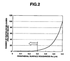
- a substrate dimensioned 520 mm x 800 mm x 10 mm (thick) was immersed in a Pyrex® tank together with a substrate holder, ultrasonic waves at 36 kHz and 200 W were applied for 10 minutes, and the number of particles released was counted by a particle counter.
- the results are plotted in FIG. 2 .
- the number of particles released is plotted on the ordinate as a relative value based on 100 for a peripheral surface roughness of 0.6 ⁇ m.
- the number of particles released increases with increasing surface roughness of the periphery and decreases with a smoother surface. Particle release is substantially suppressed by setting Ra to 0.3 ⁇ m or below. It is noted that the number of particles released from the substrate holder is subtracted from the overall number of particles.
- the major surfaces of the substrate were subjected to final polishing and then cleaned.
- the substrate was handled with gloved hands, confirming possible manual manipulation.
- An estimated coefficient of static friction was 0.12.
- the gloves used were made of polyvinyl chloride and polyethylene.
- the substrate could be equally handled in either a dry or a wet state.
- the substrate as cleaned had a satisfactory degree of cleanness, indicating few particles released.
- a rectangular synthetic quartz substrate of dimensions 700 mm ⁇ 800 mm ⁇ 8.0 mm (thick) having a weight of 9.9 kg was chamfered by a chamfering machine using #800 diamond grits, furnishing a starting substrate.
- the substrate was handled for cleaning, finding equivalent results.
- An estimated coefficient of static friction was 0.13.
- a rectangular synthetic quartz substrate of dimensions 800 mm ⁇ 920 mm ⁇ 10.0 mm (thick) having a weight of 13.0 kg was chamfered by a chamfering machine using #1200 diamond grits, furnishing a starting substrate.
- the substrate was handled for cleaning, finding equivalent results.
- An estimated coefficient of static friction was 0.16.
- the major surfaces of the substrate were subjected to final polishing and then cleaned.
- the substrate was handled with gloved hands, confirming possible manual manipulation.
- An estimated coefficient of static friction was 0.24.
- the gloves used were made of polyvinyl chloride.
- the substrate could be equally handled in either a dry or a wet state.
- the substrate as cleaned had an unsatisfactory degree of cleanness, indicating many particles released.
- the large-size substrate for light exposure of the invention has the advantage that the number of particles released from the substrate periphery during cleaning is minimized, leading to an improved yield in the cleaning step.
- the substrate can be manually handled, achieving an improvement in substrate quality without a need for a handling mechanism.
Landscapes
- Physics & Mathematics (AREA)
- General Physics & Mathematics (AREA)
- Engineering & Computer Science (AREA)
- Nonlinear Science (AREA)
- Mechanical Engineering (AREA)
- Life Sciences & Earth Sciences (AREA)
- Sustainable Development (AREA)
- Crystallography & Structural Chemistry (AREA)
- Optics & Photonics (AREA)
- Chemical & Material Sciences (AREA)
- Preparing Plates And Mask In Photomechanical Process (AREA)
- Surface Treatment Of Glass (AREA)
- Cleaning In General (AREA)
- Glass Melting And Manufacturing (AREA)
Description
- This invention relates to large-size photomask substrates adapted for light exposure for use in the manufacture of liquid crystal (LC) panels.
- In general, TFT liquid crystal panels utilize the active matrix addressing scheme in which liquid crystals are sealed between an array-side substrate having TFT devices built therein and a substrate having a color filter attached thereto, and voltages are controlled by the TFTs for controlling the alignment of liquid crystals.
- For the manufacture of the array-side substrate, plural layers are repeatedly printed on a mother glass sheet of alkali-free glass by light exposure through original plates having circuitry pattern, known as large-size photomasks. The color filter-side substrate is similarly manufactured by a lithographic process, known as dye impregnation process.
- For the manufacture of both array- and color filter-side substrates, large-size photomasks are necessary. To implement precision light exposure, synthetic quartz glass substrates having a low coefficient of linear expansion are often used for the large-size photomasks.
- When the peripheral surface of a substrate is chamfered to any shape by means of a chamfering machine, dusting from the peripheral surface becomes one of factors that govern the surface state of a finished product, especially the presence or absence of contaminants on the surface. If the peripheral surface of the substrate is rough, the contaminants deposited on the peripheral surface cannot be removed by simple cleaning. Not only some contaminants migrate and deposit on the substrate major surfaces, which in turn, requires re-cleaning or re-polishing to remove those contaminants, leading to a drop of manufacture yield.
- To solve the above and other problems, a method of mirror surface finishing the peripheral surface of a substrate of any shape is employed in the case of IC photomask substrates (see
JP-A 56-46227 - It would be desirable to be able to provide a large-size photomask substrate adapted for light exposure e.g. light transmittance which generates a minimum amount of dust from its peripheral surface during cleaning and may further allow manual handling.
- For a large-size substrate to be manually held at its peripheral surface in a wet state, it has been found that if the peripheral surface of the substrate is provided with a level of roughness to prevent the substrate from being slipped away from the handling gloves, this not only ensures safe manual holding of the substrate, but may also suppress dust generation from the peripheral surface.
- An aspect of the present invention is to provide a large-size photomask substrate adapted for light exposure, which is of a plate shape having a greatest width dimension, i.e. greatest separation between two points on the edge of the plate, e.g. a diagonal length or diameter, of at least 500 mm, a thickness of 1 to 20 mm, and a peripheral surface with a roughness Ra in the range of 0.05 to 0.4 µm.
- Preferably the peripheral surface of the photomask substrate has a coefficient of static friction with a handling glove in the presence of water of [substrate weight (kg)]/2 x (0.02 to 0.03), typically in the range of 0.1 to 0.2. Most often, the substrate is of synthetic quartz. Other aspects are the manufacture of such large-size substrates.
-
-
FIG. 1 is a graph showing a coefficient of static friction versus a peripheral surface roughness at different clamping forces. -
FIG. 2 is a graph showing the number of particles released versus a peripheral surface roughness. - The large-size photomask substrate of the invention has a plate shape, that may be embodied as a large-size synthetic quartz glass substrate. The substrate is plate-shaped, i.e. is a substantially flat member. The dimensions of the plate are chosen so that its greatest width dimension, e.g. its diagonal length or diameter is at least 500 mm, preferably 500 to 2,000 mm. The planar shape of the substrate may be square, rectangular, circular or analogous. The substrate has a thickness of 1 to 20 mm, preferably 5 to 12 mm. The substrate may have a pair of major surfaces with the peripheral or side surface(s) therebetween. The peripheral surface may be of any shape. Manual holding at the peripheral surface is favoured by a substrate in the form of a quadrangular plate, more preferably a rectangular plate, defining linear side surfaces.
- In the large-size substrate for light exposure according to the invention, the peripheral or side surface has an average surface roughness Ra in the range of 0.05 to 0.4 µm, preferably 0.05 to 0.3 µm. A peripheral surface with a Ra of less than 0.05 µm is too slippery and difficult to handle. A peripheral surface with a Ra of more than 0.4 µm can be manually handled, but releases a larger amount of dust or particles with which the substrate surface can be contaminated.
- The above-described large-size substrate for light exposure is manufactured by first chamfering the periphery of a starting large-size substrate. Chamfering is generally conducted by diamond grinding, desirably using diamond abrasives having a size of #600 to #1500.
- After chamfering to any desired shape, the substrate is lapped and the peripheral surface is then worked or finished so as to improve the surface roughness. The peripheral finishing is conducted, for example, by brushing all the periphery of the substrate by means of a peripheral quasi-mirror finishing tool. For instance, a nylon brush is rotated and the periphery of the substrate is traversed as desired. Thereafter, final polishing is conducted on the substrate major surfaces. It is noted that the peripheral finishing is typically done after the lapping step, but may be done at any other stage.
- Preferably the following considerations are taken. In the step of cleaning the substrate subsequent to the quasi-mirror finishing of its periphery, the substrate in a wet state is manipulated while clamping it only at the peripheral surfaces with human hands. The peripheral surfaces in a wet state are more slippery. The worker puts on special gloves known as handling gloves. In manipulating the substrate in a dry or wet state while holding only the peripheral surfaces with the gloved hands, the substrate can be slipped away from the gloved hands depending on the roughness of the peripheral surfaces, particularly when the roughness is approximate to a mirror finish. Handling operation is then difficult.
- If the relationship of the roughness of the substrate peripheral surface to the handling by gloved hands is determined, it becomes possible to produce an appropriate peripheral surface state to enable manual handling operation by controlling the roughness of the substrate peripheral surface by means of a peripheral quasi-mirror finishing tool. The peripheral surface state may also be sufficient to prevent dusting from the substrate periphery.
- To determine a level of roughness of the peripheral surfaces that permits the worker to hold the wet substrate only at the peripheral surfaces with gloved hands, the inventor explored the relationship of the weight of the substrate to the level of roughness of substrate peripheral surfaces below which the wet substrate at the peripheral surfaces cannot be held with gloved hands, with the results plotted in the diagram of
FIG. 1 . More particularly, a substrate having a given weight and a given roughness Ra on its peripheral surfaces was furnished. In a wet state (in the presence of water), the substrate was mounted between a pair of springs, with gloves interposed between the substrate peripheral surfaces and the springs. A certain force was applied across the opposite ends of the springs to clamp the substrate therebetween. The substrate in this state is lifted upward. The lifting force applied when the substrate started slipping was measured by a spring type tension gauge. A ratio of the lifting force to the clamping force is computed as a coefficient of static friction. It is noted that the manual clamping force inFIG. 1 is in a range of 4.5 to 5.0 kg. The surface roughness (Ra) was measured by a probe type surface roughness meter. - It is seen from the plots in
FIG. 1 that the level of surface roughness of the substrate periphery to enable handling operation is determined substantially to a fixed value that depends solely on the substrate weight. Putting these relationships in order reveals that the coefficient of static friction of a substrate at its peripheral surface may equal [substrate weight]/2 × (0.02 to 0.03). It is understood that once the weight of any substrate is known, a value for surface roughness of the substrate periphery to enable manual handling operation can be estimated from the diagram ofFIG. 1 . - As long as the surface roughness of the substrate periphery is equal to or above the thus determined value, the substrate can be handled with gloved hands independent of whether the substrate is dry or wet. For holding the substrate at its peripheral surfaces in a wet state, the value for coefficient of static friction is more predominantly governed by the surface roughness of the substrate periphery than the type of handling gloves.
- As long as the periphery of a substrate is worked to a controlled surface roughness, any substrate can be manually handled and dusting from the peripheral surface may be suppressed.
- With respect to particles generated from the substrate peripheral surface during cleaning, a substrate dimensioned 520 mm x 800 mm x 10 mm (thick) was immersed in a Pyrex® tank together with a substrate holder, ultrasonic waves at 36 kHz and 200 W were applied for 10 minutes, and the number of particles released was counted by a particle counter. The results are plotted in
FIG. 2 . The number of particles released is plotted on the ordinate as a relative value based on 100 for a peripheral surface roughness of 0.6 µm. The number of particles released increases with increasing surface roughness of the periphery and decreases with a smoother surface. Particle release is substantially suppressed by setting Ra to 0.3 µm or below. It is noted that the number of particles released from the substrate holder is subtracted from the overall number of particles. - Examples and Comparative Examples are given below for illustrating the invention, but the invention is not limited thereto.
- A rectangular synthetic quartz substrate of dimensions 520 mm × 800 mm × 10.0 mm (thick) having a weight of 9.2 kg was chamfered by a chamfering machine using #1200 diamond grits, furnishing a starting substrate. Lapping and primary polishing were carried out before the peripheral surfaces were worked. The roughness of the peripheral surfaces was measured by a probe type roughness meter, finding Ra = 0.05 µm.
- The major surfaces of the substrate were subjected to final polishing and then cleaned. In the cleaning step, the substrate was handled with gloved hands, confirming possible manual manipulation. An estimated coefficient of static friction was 0.12. The gloves used were made of polyvinyl chloride and polyethylene. The substrate could be equally handled in either a dry or a wet state. The substrate as cleaned had a satisfactory degree of cleanness, indicating few particles released.
- A rectangular synthetic quartz substrate of dimensions 700 mm × 800 mm × 8.0 mm (thick) having a weight of 9.9 kg was chamfered by a chamfering machine using #800 diamond grits, furnishing a starting substrate. The substrate was then worked as in Example 1, reaching a roughness Ra = 0.09 µm on the peripheral surfaces. As in Example 1, the substrate was handled for cleaning, finding equivalent results. An estimated coefficient of static friction was 0.13.
- A rectangular synthetic quartz substrate of dimensions 800 mm × 920 mm × 10.0 mm (thick) having a weight of 13.0 kg was chamfered by a chamfering machine using #1200 diamond grits, furnishing a starting substrate. The substrate was then worked as in Example 1, reaching a roughness Ra = 0.16 µm on the peripheral surfaces. As in Example 1, the substrate was handled for cleaning, finding equivalent results. An estimated coefficient of static friction was 0.16.
- A rectangular synthetic quartz substrate of dimensions 700 mm × 800 mm × 8.0 mm (thick) having a weight of 9.9 kg was chamfered by a chamfering machine using #800 diamond grits, furnishing a starting substrate. Lapping and primary polishing were carried out, but the subsequent peripheral surface working was omitted. The roughness of the peripheral surfaces was measured by a probe type roughness meter, finding Ra = 0.5 µm.
- The major surfaces of the substrate were subjected to final polishing and then cleaned. In the cleaning step, the substrate was handled with gloved hands, confirming possible manual manipulation. An estimated coefficient of static friction was 0.24. The gloves used were made of polyvinyl chloride. The substrate could be equally handled in either a dry or a wet state. The substrate as cleaned had an unsatisfactory degree of cleanness, indicating many particles released.
- The large-size substrate for light exposure of the invention has the advantage that the number of particles released from the substrate periphery during cleaning is minimized, leading to an improved yield in the cleaning step. The substrate can be manually handled, achieving an improvement in substrate quality without a need for a handling mechanism.
Claims (7)
- A photomask substrate in the form of a square or rectangular plate of diagonal length at least 500 mm and thickness from 1 to 20 mm, the plate having a pair of major surfaces and peripheral side surfaces between said major surfaces, said peripheral surfaces being chamfered and having an average surface roughness Ra in the range of from 0.05 to 0.4 µm.
- A photomask substrate of claim 1 which is from 5 to 20 mm thick.
- A photomask substrate according to claim 1 or 2 which is of synthetic quartz.
- Method of processing a photomask substrate having a plate shape, a diagonal length or diameter of at least 500 mm, a pair of major surfaces and a peripheral surface between the major surfaces, the method comprising handling the photomask substrate with a handling glove, wherein the peripheral surface has a roughness Ra in the range from 0.05 to 0.4 µm and the coefficient of static friction between said peripheral surface of the substrate and the handling glove in the presence of water being [substrate weight (kg)1/2 x (0.02 to 0.03).
- A method of claim 4 in which said coefficient of static friction with the handling glove is from 0.1 to 0.2.
- A method of claim 4 in which the handling glove is made from polyvinyl chloride or polyethylene.
- A method of claim 4, 5 or 6 in which said handling is during a step of cleaning the photomask substrate, after the working or finishing of said peripheral surface thereof to said roughness and conducting final polishing on the major surfaces.
Applications Claiming Priority (2)
| Application Number | Priority Date | Filing Date | Title |
|---|---|---|---|
| JP2003199004 | 2003-07-18 | ||
| JP2003199004A JP4206850B2 (en) | 2003-07-18 | 2003-07-18 | Manufacturing method of large synthetic quartz glass substrate for exposure |
Publications (3)
| Publication Number | Publication Date |
|---|---|
| EP1498775A2 EP1498775A2 (en) | 2005-01-19 |
| EP1498775A3 EP1498775A3 (en) | 2006-10-04 |
| EP1498775B1 true EP1498775B1 (en) | 2010-09-22 |
Family
ID=33475522
Family Applications (1)
| Application Number | Title | Priority Date | Filing Date |
|---|---|---|---|
| EP04254320A Expired - Lifetime EP1498775B1 (en) | 2003-07-18 | 2004-07-19 | Large-size substrate for photolithographic applications |
Country Status (7)
| Country | Link |
|---|---|
| US (1) | US8012563B2 (en) |
| EP (1) | EP1498775B1 (en) |
| JP (1) | JP4206850B2 (en) |
| KR (1) | KR100853613B1 (en) |
| CN (1) | CN100514162C (en) |
| DE (1) | DE602004029223D1 (en) |
| TW (1) | TW200510260A (en) |
Families Citing this family (11)
| Publication number | Priority date | Publication date | Assignee | Title |
|---|---|---|---|---|
| JP4362732B2 (en) * | 2005-06-17 | 2009-11-11 | 信越化学工業株式会社 | Large glass substrate for photomask and manufacturing method thereof, computer-readable recording medium, and mother glass exposure method |
| JP5484649B2 (en) * | 2006-01-27 | 2014-05-07 | 古河電気工業株式会社 | Thin glass manufacturing method |
| JP5414079B2 (en) * | 2006-05-15 | 2014-02-12 | Hoya株式会社 | FPD device manufacturing mask blank, photomask, and FPD device manufacturing mask blank design method |
| CN101522584B (en) * | 2006-10-10 | 2012-12-05 | 日本电气硝子株式会社 | Tempered glass substrate |
| US7666508B2 (en) * | 2007-05-22 | 2010-02-23 | Corning Incorporated | Glass article having a laser melted surface |
| US8062732B2 (en) * | 2007-05-22 | 2011-11-22 | Corning Incorporated | Glass article having improved edge |
| CN101903301B (en) * | 2007-12-18 | 2012-12-19 | Hoya株式会社 | Protective glass for portable terminal, manufacturing method thereof, and portable terminal device |
| CN102317860B (en) * | 2009-02-13 | 2013-07-03 | Hoya株式会社 | Substrate for mask blank use, mask blank, and photo mask |
| CN102341214B (en) * | 2009-03-10 | 2015-01-28 | 日本电气硝子株式会社 | Glass substrate and method for manufacturing same |
| JP2014023196A (en) * | 2012-07-13 | 2014-02-03 | Denso Corp | Motor control device |
| JP6727170B2 (en) * | 2017-06-30 | 2020-07-22 | クアーズテック株式会社 | Substrate for photomask |
Family Cites Families (18)
| Publication number | Priority date | Publication date | Assignee | Title |
|---|---|---|---|---|
| JPS5646227A (en) | 1979-09-21 | 1981-04-27 | Shin Etsu Chem Co Ltd | Mask substrate for electronic device |
| JPH02204345A (en) | 1989-01-31 | 1990-08-14 | Hoya Corp | Glass substrate |
| EP0598349B1 (en) * | 1992-11-19 | 1998-07-29 | Shin-Etsu Quartz Products Co., Ltd. | Process for manufacturing a large sized quartz glass tube, a preform and an optical fiber |
| US5773126A (en) * | 1994-12-22 | 1998-06-30 | Dai Nippon Printing Co., Ltd. | Composite film having a surface slip property |
| US5961197A (en) * | 1995-12-14 | 1999-10-05 | Enplas Corporation | Surface light source device |
| US5643365A (en) * | 1996-07-25 | 1997-07-01 | Ceram Optec Industries Inc | Method and device for plasma vapor chemical deposition of homogeneous films on large flat surfaces |
| US5816897A (en) * | 1996-09-16 | 1998-10-06 | Corning Incorporated | Method and apparatus for edge finishing glass |
| JP2000218481A (en) * | 1999-01-27 | 2000-08-08 | Nippon Sheet Glass Co Ltd | Method of removing streak-like concavities and convexities from glass pane surface, and glass pane reduced in streak-like concavities and covexities |
| JP2000267253A (en) | 1999-03-12 | 2000-09-29 | Seiko Epson Corp | Method of forming exposure mask and method of manufacturing liquid crystal device |
| US6506289B2 (en) * | 2000-08-07 | 2003-01-14 | Symmorphix, Inc. | Planar optical devices and methods for their manufacture |
| JP3516233B2 (en) * | 2000-11-06 | 2004-04-05 | 日本板硝子株式会社 | Manufacturing method of glass substrate for information recording medium |
| JP4561950B2 (en) * | 2001-08-08 | 2010-10-13 | 信越化学工業株式会社 | Square substrate |
| JP2003089550A (en) * | 2001-09-13 | 2003-03-28 | Fujikura Ltd | Glass material polishing method and fiber preform manufacturing method using the same |
| JP2003173015A (en) | 2001-09-28 | 2003-06-20 | Hoya Corp | Method of manufacturing gray tone mask |
| TWI250133B (en) * | 2002-01-31 | 2006-03-01 | Shinetsu Chemical Co | Large-sized substrate and method of producing the same |
| US7323276B2 (en) * | 2003-03-26 | 2008-01-29 | Hoya Corporation | Substrate for photomask, photomask blank and photomask |
| JP3934115B2 (en) | 2003-03-26 | 2007-06-20 | Hoya株式会社 | Photomask substrate, photomask blank, and photomask |
| US6910953B2 (en) * | 2003-07-24 | 2005-06-28 | Corning Incorporated | Methods and apparatus for edge finishing glass sheets |
-
2003
- 2003-07-18 JP JP2003199004A patent/JP4206850B2/en not_active Expired - Lifetime
-
2004
- 2004-07-15 US US10/891,028 patent/US8012563B2/en not_active Expired - Lifetime
- 2004-07-16 CN CNB2004100712695A patent/CN100514162C/en not_active Expired - Lifetime
- 2004-07-16 TW TW093121379A patent/TW200510260A/en not_active IP Right Cessation
- 2004-07-16 KR KR1020040055461A patent/KR100853613B1/en not_active Expired - Lifetime
- 2004-07-19 DE DE602004029223T patent/DE602004029223D1/en not_active Expired - Lifetime
- 2004-07-19 EP EP04254320A patent/EP1498775B1/en not_active Expired - Lifetime
Also Published As
| Publication number | Publication date |
|---|---|
| CN100514162C (en) | 2009-07-15 |
| DE602004029223D1 (en) | 2010-11-04 |
| CN1577029A (en) | 2005-02-09 |
| KR100853613B1 (en) | 2008-08-22 |
| KR20050009690A (en) | 2005-01-25 |
| EP1498775A3 (en) | 2006-10-04 |
| TW200510260A (en) | 2005-03-16 |
| EP1498775A2 (en) | 2005-01-19 |
| JP4206850B2 (en) | 2009-01-14 |
| US8012563B2 (en) | 2011-09-06 |
| US20050013972A1 (en) | 2005-01-20 |
| TWI353968B (en) | 2011-12-11 |
| JP2005037580A (en) | 2005-02-10 |
Similar Documents
| Publication | Publication Date | Title |
|---|---|---|
| CN102314082B (en) | For the manufacture of the method for electronic grade synthetic quartz glass substrate | |
| US8012563B2 (en) | Large-size substrate | |
| TW308561B (en) | ||
| DE69429122T2 (en) | Process for protecting the surface of a semiconducting substrate during grinding | |
| JP2009173542A (en) | Processing method of synthetic quartz glass substrate | |
| CN102317860B (en) | Substrate for mask blank use, mask blank, and photo mask | |
| TWI680347B (en) | Photomask substrate, photomask blank, photomask, method of manufacturing a photomask substrate, method of manufacturing a photomask, and method of manufacturing a display device | |
| CN113851153B (en) | Spacer, laminate of substrates, and method for manufacturing substrates | |
| JP2012027176A (en) | Substrate for photomask | |
| KR100541376B1 (en) | Substrate for photomask, photomask blank and photomask | |
| KR100690098B1 (en) | Polishing method of semiconductor wafer and polishing apparatus of semiconductor wafer | |
| KR20100109864A (en) | Method for producing large-size synthetic quartz glass substrate | |
| JP3934115B2 (en) | Photomask substrate, photomask blank, and photomask | |
| KR20120074328A (en) | Low-expansion glass substrate for a reflective mask and reflective mask | |
| JP4883322B2 (en) | Large synthetic quartz glass substrate for exposure | |
| JP2015214449A (en) | Glass substrate manufacturing method and glass substrate | |
| JP5365137B2 (en) | Photomask substrate and manufacturing method thereof | |
| JP6973280B2 (en) | Synthetic quartz glass substrate for imprint mold | |
| JP3329594B2 (en) | Method of manufacturing sapphire substrate for photomask | |
| JP4435500B2 (en) | Substrate double-side polishing method, double-side polishing guide ring and substrate double-side polishing apparatus | |
| JPH04116658A (en) | Substrate for photomask | |
| KR20110127571A (en) | Transparent substrates for photomask blanks, photomask blanks and photomasks | |
| KR101437326B1 (en) | Transparent Substrate for Blankmask and Photomask | |
| Karow | The Influence of Substrate Preparation on Optical Coatings |
Legal Events
| Date | Code | Title | Description |
|---|---|---|---|
| PUAI | Public reference made under article 153(3) epc to a published international application that has entered the european phase |
Free format text: ORIGINAL CODE: 0009012 |
|
| AK | Designated contracting states |
Kind code of ref document: A2 Designated state(s): AT BE BG CH CY CZ DE DK EE ES FI FR GB GR HU IE IT LI LU MC NL PL PT RO SE SI SK TR |
|
| AX | Request for extension of the european patent |
Extension state: AL HR LT LV MK |
|
| PUAL | Search report despatched |
Free format text: ORIGINAL CODE: 0009013 |
|
| AK | Designated contracting states |
Kind code of ref document: A3 Designated state(s): AT BE BG CH CY CZ DE DK EE ES FI FR GB GR HU IE IT LI LU MC NL PL PT RO SE SI SK TR |
|
| AX | Request for extension of the european patent |
Extension state: AL HR LT LV MK |
|
| 17P | Request for examination filed |
Effective date: 20070117 |
|
| AKX | Designation fees paid |
Designated state(s): DE FR GB |
|
| 17Q | First examination report despatched |
Effective date: 20070724 |
|
| GRAP | Despatch of communication of intention to grant a patent |
Free format text: ORIGINAL CODE: EPIDOSNIGR1 |
|
| GRAS | Grant fee paid |
Free format text: ORIGINAL CODE: EPIDOSNIGR3 |
|
| GRAA | (expected) grant |
Free format text: ORIGINAL CODE: 0009210 |
|
| AK | Designated contracting states |
Kind code of ref document: B1 Designated state(s): DE FR GB |
|
| REG | Reference to a national code |
Ref country code: GB Ref legal event code: FG4D |
|
| REF | Corresponds to: |
Ref document number: 602004029223 Country of ref document: DE Date of ref document: 20101104 Kind code of ref document: P |
|
| PLBE | No opposition filed within time limit |
Free format text: ORIGINAL CODE: 0009261 |
|
| STAA | Information on the status of an ep patent application or granted ep patent |
Free format text: STATUS: NO OPPOSITION FILED WITHIN TIME LIMIT |
|
| 26N | No opposition filed |
Effective date: 20110623 |
|
| REG | Reference to a national code |
Ref country code: DE Ref legal event code: R097 Ref document number: 602004029223 Country of ref document: DE Effective date: 20110623 |
|
| REG | Reference to a national code |
Ref country code: FR Ref legal event code: PLFP Year of fee payment: 13 |
|
| REG | Reference to a national code |
Ref country code: FR Ref legal event code: PLFP Year of fee payment: 14 |
|
| REG | Reference to a national code |
Ref country code: FR Ref legal event code: PLFP Year of fee payment: 15 |
|
| PGFP | Annual fee paid to national office [announced via postgrant information from national office to epo] |
Ref country code: FR Payment date: 20230620 Year of fee payment: 20 |
|
| PGFP | Annual fee paid to national office [announced via postgrant information from national office to epo] |
Ref country code: GB Payment date: 20230601 Year of fee payment: 20 |
|
| PGFP | Annual fee paid to national office [announced via postgrant information from national office to epo] |
Ref country code: DE Payment date: 20230531 Year of fee payment: 20 |
|
| REG | Reference to a national code |
Ref country code: DE Ref legal event code: R071 Ref document number: 602004029223 Country of ref document: DE |
|
| REG | Reference to a national code |
Ref country code: GB Ref legal event code: PE20 Expiry date: 20240718 |
|
| PG25 | Lapsed in a contracting state [announced via postgrant information from national office to epo] |
Ref country code: GB Free format text: LAPSE BECAUSE OF EXPIRATION OF PROTECTION Effective date: 20240718 |
|
| PG25 | Lapsed in a contracting state [announced via postgrant information from national office to epo] |
Ref country code: GB Free format text: LAPSE BECAUSE OF EXPIRATION OF PROTECTION Effective date: 20240718 |