EP1496493A2 - Display panel driving method - Google Patents
Display panel driving method Download PDFInfo
- Publication number
- EP1496493A2 EP1496493A2 EP04014740A EP04014740A EP1496493A2 EP 1496493 A2 EP1496493 A2 EP 1496493A2 EP 04014740 A EP04014740 A EP 04014740A EP 04014740 A EP04014740 A EP 04014740A EP 1496493 A2 EP1496493 A2 EP 1496493A2
- Authority
- EP
- European Patent Office
- Prior art keywords
- display
- subfield
- subfields
- display line
- light emission
- Prior art date
- Legal status (The legal status is an assumption and is not a legal conclusion. Google has not performed a legal analysis and makes no representation as to the accuracy of the status listed.)
- Withdrawn
Links
Images













Classifications
-
- G—PHYSICS
- G09—EDUCATION; CRYPTOGRAPHY; DISPLAY; ADVERTISING; SEALS
- G09G—ARRANGEMENTS OR CIRCUITS FOR CONTROL OF INDICATING DEVICES USING STATIC MEANS TO PRESENT VARIABLE INFORMATION
- G09G3/00—Control arrangements or circuits, of interest only in connection with visual indicators other than cathode-ray tubes
- G09G3/20—Control arrangements or circuits, of interest only in connection with visual indicators other than cathode-ray tubes for presentation of an assembly of a number of characters, e.g. a page, by composing the assembly by combination of individual elements arranged in a matrix no fixed position being assigned to or needed to be assigned to the individual characters or partial characters
- G09G3/22—Control arrangements or circuits, of interest only in connection with visual indicators other than cathode-ray tubes for presentation of an assembly of a number of characters, e.g. a page, by composing the assembly by combination of individual elements arranged in a matrix no fixed position being assigned to or needed to be assigned to the individual characters or partial characters using controlled light sources
- G09G3/28—Control arrangements or circuits, of interest only in connection with visual indicators other than cathode-ray tubes for presentation of an assembly of a number of characters, e.g. a page, by composing the assembly by combination of individual elements arranged in a matrix no fixed position being assigned to or needed to be assigned to the individual characters or partial characters using controlled light sources using luminous gas-discharge panels, e.g. plasma panels
- G09G3/288—Control arrangements or circuits, of interest only in connection with visual indicators other than cathode-ray tubes for presentation of an assembly of a number of characters, e.g. a page, by composing the assembly by combination of individual elements arranged in a matrix no fixed position being assigned to or needed to be assigned to the individual characters or partial characters using controlled light sources using luminous gas-discharge panels, e.g. plasma panels using AC panels
- G09G3/291—Control arrangements or circuits, of interest only in connection with visual indicators other than cathode-ray tubes for presentation of an assembly of a number of characters, e.g. a page, by composing the assembly by combination of individual elements arranged in a matrix no fixed position being assigned to or needed to be assigned to the individual characters or partial characters using controlled light sources using luminous gas-discharge panels, e.g. plasma panels using AC panels controlling the gas discharge to control a cell condition, e.g. by means of specific pulse shapes
-
- G—PHYSICS
- G09—EDUCATION; CRYPTOGRAPHY; DISPLAY; ADVERTISING; SEALS
- G09G—ARRANGEMENTS OR CIRCUITS FOR CONTROL OF INDICATING DEVICES USING STATIC MEANS TO PRESENT VARIABLE INFORMATION
- G09G3/00—Control arrangements or circuits, of interest only in connection with visual indicators other than cathode-ray tubes
- G09G3/20—Control arrangements or circuits, of interest only in connection with visual indicators other than cathode-ray tubes for presentation of an assembly of a number of characters, e.g. a page, by composing the assembly by combination of individual elements arranged in a matrix no fixed position being assigned to or needed to be assigned to the individual characters or partial characters
- G09G3/22—Control arrangements or circuits, of interest only in connection with visual indicators other than cathode-ray tubes for presentation of an assembly of a number of characters, e.g. a page, by composing the assembly by combination of individual elements arranged in a matrix no fixed position being assigned to or needed to be assigned to the individual characters or partial characters using controlled light sources
- G09G3/28—Control arrangements or circuits, of interest only in connection with visual indicators other than cathode-ray tubes for presentation of an assembly of a number of characters, e.g. a page, by composing the assembly by combination of individual elements arranged in a matrix no fixed position being assigned to or needed to be assigned to the individual characters or partial characters using controlled light sources using luminous gas-discharge panels, e.g. plasma panels
- G09G3/288—Control arrangements or circuits, of interest only in connection with visual indicators other than cathode-ray tubes for presentation of an assembly of a number of characters, e.g. a page, by composing the assembly by combination of individual elements arranged in a matrix no fixed position being assigned to or needed to be assigned to the individual characters or partial characters using controlled light sources using luminous gas-discharge panels, e.g. plasma panels using AC panels
- G09G3/291—Control arrangements or circuits, of interest only in connection with visual indicators other than cathode-ray tubes for presentation of an assembly of a number of characters, e.g. a page, by composing the assembly by combination of individual elements arranged in a matrix no fixed position being assigned to or needed to be assigned to the individual characters or partial characters using controlled light sources using luminous gas-discharge panels, e.g. plasma panels using AC panels controlling the gas discharge to control a cell condition, e.g. by means of specific pulse shapes
- G09G3/293—Control arrangements or circuits, of interest only in connection with visual indicators other than cathode-ray tubes for presentation of an assembly of a number of characters, e.g. a page, by composing the assembly by combination of individual elements arranged in a matrix no fixed position being assigned to or needed to be assigned to the individual characters or partial characters using controlled light sources using luminous gas-discharge panels, e.g. plasma panels using AC panels controlling the gas discharge to control a cell condition, e.g. by means of specific pulse shapes for address discharge
- G09G3/2935—Addressed by erasing selected cells that are in an ON state
-
- G—PHYSICS
- G09—EDUCATION; CRYPTOGRAPHY; DISPLAY; ADVERTISING; SEALS
- G09G—ARRANGEMENTS OR CIRCUITS FOR CONTROL OF INDICATING DEVICES USING STATIC MEANS TO PRESENT VARIABLE INFORMATION
- G09G3/00—Control arrangements or circuits, of interest only in connection with visual indicators other than cathode-ray tubes
- G09G3/20—Control arrangements or circuits, of interest only in connection with visual indicators other than cathode-ray tubes for presentation of an assembly of a number of characters, e.g. a page, by composing the assembly by combination of individual elements arranged in a matrix no fixed position being assigned to or needed to be assigned to the individual characters or partial characters
- G09G3/2007—Display of intermediate tones
- G09G3/2018—Display of intermediate tones by time modulation using two or more time intervals
- G09G3/2022—Display of intermediate tones by time modulation using two or more time intervals using sub-frames
- G09G3/2029—Display of intermediate tones by time modulation using two or more time intervals using sub-frames the sub-frames having non-binary weights
-
- G—PHYSICS
- G09—EDUCATION; CRYPTOGRAPHY; DISPLAY; ADVERTISING; SEALS
- G09G—ARRANGEMENTS OR CIRCUITS FOR CONTROL OF INDICATING DEVICES USING STATIC MEANS TO PRESENT VARIABLE INFORMATION
- G09G3/00—Control arrangements or circuits, of interest only in connection with visual indicators other than cathode-ray tubes
- G09G3/20—Control arrangements or circuits, of interest only in connection with visual indicators other than cathode-ray tubes for presentation of an assembly of a number of characters, e.g. a page, by composing the assembly by combination of individual elements arranged in a matrix no fixed position being assigned to or needed to be assigned to the individual characters or partial characters
- G09G3/2007—Display of intermediate tones
- G09G3/2018—Display of intermediate tones by time modulation using two or more time intervals
- G09G3/2022—Display of intermediate tones by time modulation using two or more time intervals using sub-frames
- G09G3/2037—Display of intermediate tones by time modulation using two or more time intervals using sub-frames with specific control of sub-frames corresponding to the least significant bits
-
- G—PHYSICS
- G09—EDUCATION; CRYPTOGRAPHY; DISPLAY; ADVERTISING; SEALS
- G09G—ARRANGEMENTS OR CIRCUITS FOR CONTROL OF INDICATING DEVICES USING STATIC MEANS TO PRESENT VARIABLE INFORMATION
- G09G3/00—Control arrangements or circuits, of interest only in connection with visual indicators other than cathode-ray tubes
- G09G3/20—Control arrangements or circuits, of interest only in connection with visual indicators other than cathode-ray tubes for presentation of an assembly of a number of characters, e.g. a page, by composing the assembly by combination of individual elements arranged in a matrix no fixed position being assigned to or needed to be assigned to the individual characters or partial characters
- G09G3/2007—Display of intermediate tones
- G09G3/2018—Display of intermediate tones by time modulation using two or more time intervals
- G09G3/2022—Display of intermediate tones by time modulation using two or more time intervals using sub-frames
- G09G3/204—Display of intermediate tones by time modulation using two or more time intervals using sub-frames the sub-frames being organized in consecutive sub-frame groups
-
- G—PHYSICS
- G09—EDUCATION; CRYPTOGRAPHY; DISPLAY; ADVERTISING; SEALS
- G09G—ARRANGEMENTS OR CIRCUITS FOR CONTROL OF INDICATING DEVICES USING STATIC MEANS TO PRESENT VARIABLE INFORMATION
- G09G3/00—Control arrangements or circuits, of interest only in connection with visual indicators other than cathode-ray tubes
- G09G3/20—Control arrangements or circuits, of interest only in connection with visual indicators other than cathode-ray tubes for presentation of an assembly of a number of characters, e.g. a page, by composing the assembly by combination of individual elements arranged in a matrix no fixed position being assigned to or needed to be assigned to the individual characters or partial characters
- G09G3/2007—Display of intermediate tones
- G09G3/2044—Display of intermediate tones using dithering
- G09G3/2051—Display of intermediate tones using dithering with use of a spatial dither pattern
- G09G3/2055—Display of intermediate tones using dithering with use of a spatial dither pattern the pattern being varied in time
-
- G—PHYSICS
- G09—EDUCATION; CRYPTOGRAPHY; DISPLAY; ADVERTISING; SEALS
- G09G—ARRANGEMENTS OR CIRCUITS FOR CONTROL OF INDICATING DEVICES USING STATIC MEANS TO PRESENT VARIABLE INFORMATION
- G09G3/00—Control arrangements or circuits, of interest only in connection with visual indicators other than cathode-ray tubes
- G09G3/20—Control arrangements or circuits, of interest only in connection with visual indicators other than cathode-ray tubes for presentation of an assembly of a number of characters, e.g. a page, by composing the assembly by combination of individual elements arranged in a matrix no fixed position being assigned to or needed to be assigned to the individual characters or partial characters
- G09G3/2007—Display of intermediate tones
- G09G3/2077—Display of intermediate tones by a combination of two or more gradation control methods
-
- G—PHYSICS
- G09—EDUCATION; CRYPTOGRAPHY; DISPLAY; ADVERTISING; SEALS
- G09G—ARRANGEMENTS OR CIRCUITS FOR CONTROL OF INDICATING DEVICES USING STATIC MEANS TO PRESENT VARIABLE INFORMATION
- G09G3/00—Control arrangements or circuits, of interest only in connection with visual indicators other than cathode-ray tubes
- G09G3/20—Control arrangements or circuits, of interest only in connection with visual indicators other than cathode-ray tubes for presentation of an assembly of a number of characters, e.g. a page, by composing the assembly by combination of individual elements arranged in a matrix no fixed position being assigned to or needed to be assigned to the individual characters or partial characters
- G09G3/22—Control arrangements or circuits, of interest only in connection with visual indicators other than cathode-ray tubes for presentation of an assembly of a number of characters, e.g. a page, by composing the assembly by combination of individual elements arranged in a matrix no fixed position being assigned to or needed to be assigned to the individual characters or partial characters using controlled light sources
- G09G3/28—Control arrangements or circuits, of interest only in connection with visual indicators other than cathode-ray tubes for presentation of an assembly of a number of characters, e.g. a page, by composing the assembly by combination of individual elements arranged in a matrix no fixed position being assigned to or needed to be assigned to the individual characters or partial characters using controlled light sources using luminous gas-discharge panels, e.g. plasma panels
- G09G3/288—Control arrangements or circuits, of interest only in connection with visual indicators other than cathode-ray tubes for presentation of an assembly of a number of characters, e.g. a page, by composing the assembly by combination of individual elements arranged in a matrix no fixed position being assigned to or needed to be assigned to the individual characters or partial characters using controlled light sources using luminous gas-discharge panels, e.g. plasma panels using AC panels
- G09G3/291—Control arrangements or circuits, of interest only in connection with visual indicators other than cathode-ray tubes for presentation of an assembly of a number of characters, e.g. a page, by composing the assembly by combination of individual elements arranged in a matrix no fixed position being assigned to or needed to be assigned to the individual characters or partial characters using controlled light sources using luminous gas-discharge panels, e.g. plasma panels using AC panels controlling the gas discharge to control a cell condition, e.g. by means of specific pulse shapes
- G09G3/292—Control arrangements or circuits, of interest only in connection with visual indicators other than cathode-ray tubes for presentation of an assembly of a number of characters, e.g. a page, by composing the assembly by combination of individual elements arranged in a matrix no fixed position being assigned to or needed to be assigned to the individual characters or partial characters using controlled light sources using luminous gas-discharge panels, e.g. plasma panels using AC panels controlling the gas discharge to control a cell condition, e.g. by means of specific pulse shapes for reset discharge, priming discharge or erase discharge occurring in a phase other than addressing
- G09G3/2927—Details of initialising
-
- G—PHYSICS
- G09—EDUCATION; CRYPTOGRAPHY; DISPLAY; ADVERTISING; SEALS
- G09G—ARRANGEMENTS OR CIRCUITS FOR CONTROL OF INDICATING DEVICES USING STATIC MEANS TO PRESENT VARIABLE INFORMATION
- G09G3/00—Control arrangements or circuits, of interest only in connection with visual indicators other than cathode-ray tubes
- G09G3/20—Control arrangements or circuits, of interest only in connection with visual indicators other than cathode-ray tubes for presentation of an assembly of a number of characters, e.g. a page, by composing the assembly by combination of individual elements arranged in a matrix no fixed position being assigned to or needed to be assigned to the individual characters or partial characters
- G09G3/22—Control arrangements or circuits, of interest only in connection with visual indicators other than cathode-ray tubes for presentation of an assembly of a number of characters, e.g. a page, by composing the assembly by combination of individual elements arranged in a matrix no fixed position being assigned to or needed to be assigned to the individual characters or partial characters using controlled light sources
- G09G3/28—Control arrangements or circuits, of interest only in connection with visual indicators other than cathode-ray tubes for presentation of an assembly of a number of characters, e.g. a page, by composing the assembly by combination of individual elements arranged in a matrix no fixed position being assigned to or needed to be assigned to the individual characters or partial characters using controlled light sources using luminous gas-discharge panels, e.g. plasma panels
- G09G3/288—Control arrangements or circuits, of interest only in connection with visual indicators other than cathode-ray tubes for presentation of an assembly of a number of characters, e.g. a page, by composing the assembly by combination of individual elements arranged in a matrix no fixed position being assigned to or needed to be assigned to the individual characters or partial characters using controlled light sources using luminous gas-discharge panels, e.g. plasma panels using AC panels
- G09G3/291—Control arrangements or circuits, of interest only in connection with visual indicators other than cathode-ray tubes for presentation of an assembly of a number of characters, e.g. a page, by composing the assembly by combination of individual elements arranged in a matrix no fixed position being assigned to or needed to be assigned to the individual characters or partial characters using controlled light sources using luminous gas-discharge panels, e.g. plasma panels using AC panels controlling the gas discharge to control a cell condition, e.g. by means of specific pulse shapes
- G09G3/293—Control arrangements or circuits, of interest only in connection with visual indicators other than cathode-ray tubes for presentation of an assembly of a number of characters, e.g. a page, by composing the assembly by combination of individual elements arranged in a matrix no fixed position being assigned to or needed to be assigned to the individual characters or partial characters using controlled light sources using luminous gas-discharge panels, e.g. plasma panels using AC panels controlling the gas discharge to control a cell condition, e.g. by means of specific pulse shapes for address discharge
- G09G3/2932—Addressed by writing selected cells that are in an OFF state
-
- G—PHYSICS
- G09—EDUCATION; CRYPTOGRAPHY; DISPLAY; ADVERTISING; SEALS
- G09G—ARRANGEMENTS OR CIRCUITS FOR CONTROL OF INDICATING DEVICES USING STATIC MEANS TO PRESENT VARIABLE INFORMATION
- G09G2310/00—Command of the display device
- G09G2310/02—Addressing, scanning or driving the display screen or processing steps related thereto
- G09G2310/0202—Addressing of scan or signal lines
- G09G2310/0218—Addressing of scan or signal lines with collection of electrodes in groups for n-dimensional addressing
-
- G—PHYSICS
- G09—EDUCATION; CRYPTOGRAPHY; DISPLAY; ADVERTISING; SEALS
- G09G—ARRANGEMENTS OR CIRCUITS FOR CONTROL OF INDICATING DEVICES USING STATIC MEANS TO PRESENT VARIABLE INFORMATION
- G09G2320/00—Control of display operating conditions
- G09G2320/02—Improving the quality of display appearance
- G09G2320/0247—Flicker reduction other than flicker reduction circuits used for single beam cathode-ray tubes
Definitions
- the present invention relates to a driving method for a display panel that has a multiple grayscale processing circuit that subjects a video input signal to multiple grayscale processing.
- the subfield method is known as a driving method for displaying an image corresponding with a video input signal on the PDP.
- the subfield method divides a single-field display period into a plurality of subfields and causes each of the discharge cells to selectively discharge light in each subfield in accordance with the luminance level represented by the video input signal. Accordingly, an intermediate luminance corresponding with the total light emission period within the single-field period is then visible.
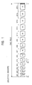
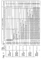
- Fig. 1 of the attached drawings shows an example of a light emission drive sequence based on this subfield method.
- This emission drive sequence is disclosed in, for example, Japanese Patent Application Kokai (Laid-Open Publication) No. 2000-227778.
- the light emission drive sequence shown in Fig. 1 divides a single field period into 14 subfields, which are the subfields SF1 to SF14. All the discharge cells of the PDP are initialized in lit mode only in the leading subfield SF1 of these subfields SF1 to SF14 (Rc). Each of the subfields SF1 to SF14 sets some of the discharge cells to unlit mode in accordance with the video input signal (Wc) and causes only the discharge cells of lit mode to discharge light over the period allocated to the subfield concerned (Ic).
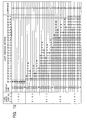
- Fig. 2 of the attached drawings shows an example of a light emission drive pattern in a single field period of each discharge cell that is driven on the basis of this light emission drive sequence (see Japanese Patent Application Kokai No. 2000-2277785).
- the discharge cells initialized in lit mode in the leading subfield SF1 are then set to unlit mode in a particular one subfield of the subfields SF1 to SF14, as indicated by the black circles.
- the discharge cell does not re-enter lit mode until the one field period ends.
- the discharge cells discharge light continuously in these subfields.
- each of the fifteen different light emission patterns shown in Fig. 2 has a different total light emission period within a single field period, and hence fifteen different intermediate luminances are rendered. That is, an intermediate luminance display for (N+1) grayscales (N being the number of subfields) is feasible.
- Error diffusion processing converts the video input signal into 8-bit pixel data, for example, for each pixel.
- the upper 6 bits of the pixel data is treated as display data and the remaining lower two bits of the pixel data is treated as error data.
- the error data of the pixel data are weighted and added based on the respective peripheral pixels and the resultant is reflected in the display data.
- a pseudo-representation of the luminance of the lower two bits of the original pixel is provided by the peripheral pixels, and, consequently, a luminance grayscale representation of the 8 bits of pixel data is possible by means of the six bits of display data.
- dither processing is performed on the six-bit error-diffusion-processed pixel data obtained by the error diffusion processing.
- a single pixel unit is rendered from a plurality of adjoining pixels, and dither coefficients consisting of different coefficient values are allocated and added to the error-diffusion-processed pixel data corresponding with the respective pixels in the single pixel unit.
- the luminance of the 8-bit original data can be represented by only the upper four bits of the dither-added pixel data. Therefore, the upper four bits of the dither-added pixel data are extracted and allocated to each of the 15 different light emission patterns shown in Fig. 2 as multiple grayscale pixel data PDs.
- a dither coefficient addition is performed regularly on the pixel data by means of dither processing and so forth, a pseudo pattern which is completely independent of the video input signal, i.e. a so-called dither pattern, is sometimes observed, which compromises the quality of the displayed image.
- the switching frequency is the same as the vertical synchronization frequency for a single field display period. Accordingly, when a PAL television signal whose vertical synchronization frequency is only 50Hz is supplied as the video input signal, flicker is prominent.
- An object of the present invention is to provide a display panel driving method that can produce an improved image display in which flicker and dither patterns are suppressed.
- an improved driving method to performs grayscale driving of a display panel in accordance with pixel data derived from on a video input signal.
- the display panel includes pixel cells arranged on each of display lines of the display panel.
- the display lines are divided into a plurality of display line groups, and each display line group consists of a plurality of adjacent display lines.
- the driving method includes a light emission driving step in which, in accordance with the pixel data, the pixel cells arranged on the display lines in the display line group concerned are made to emit light continuously over different light emission periods based on weighting values allocated to the display lines in the display line group concerned, for each field display period of the video signal.
- Each of the light emission periods is divided into two parts such that one part takes place in a first-half period of the field display period concerned and another part takes place in a second-half period of the field display period concerned. Each part starts from a reset step.
- the PDP 100 includes a front-side substrate (not shown) that functions as a display surface, and a rear-side substrate (not shown) that is disposed in a position opposite the front-side substrate.
- a discharge space filled with discharge gas is defined between the front-side substrate and rear-side substrate.
- Belt-shaped row electrodes X 1 to X n and row electrodes Y 1 to Y n are alternately arranged in parallel to each other and provided on the front-side substrate.
- Belt-shaped column electrodes D 1 to D m arranged to cross over the row electrodes are provided on the rear-side substrate.
- the row electrodes X 1 to X n and Y 1 to Y n are arranged such that the first to nth display lines of the PDP 100 are defined by n pairs of row electrodes X i and Y i .
- Discharge cells G serving as pixels are formed at the intersection points (including the discharge space) between the row electrode pairs and column electrodes. That is, (n ⁇ m) discharge cells G (1,1) to G (n,m) are formed in a matrix shape on the PDP 100.
- a pixel data conversion circuit 1 converts a video input signal into 6-bit pixel data PD, for example, for each pixel, and then supplies this pixel data PD to a multiple grayscale processing circuit 2.
- the multiple grayscale processing circuit 2 includes a line dither offset value generation circuit 21, an adder 22, and a lower bit discard circuit 23.
- the line dither offset value generation circuit 21 first generates eight line dither offset values LD with the values '0' to '7' respectively to match eight display line groups of the PDP 100.
- the first to nth display lines of the PDP 100 are separated by eight lines and grouped as shown below:
- N is a natural number equal to or less than (1/8) ⁇ n.
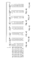
- the line dither offset value generation circuit 21 repeatedly executes, for each field and with 8 fields forming one cycle, the alteration of allocation of the line dither offset values LD to the display line groups, as shown in Figs. 4A to 4H.
- the line dither offset value generation circuit 21 allocates, in the very first field, the following line dither offset values LD to the eight display line groups:
- the line dither offset values LD are allocated in the second field:
- the line dither offset values LD are allocated in the third field:
- the line dither offset values LD with the following values are allocated in the fourth field:
- the line dither offset values LD are allocated in the seventh field:
- the line dither offset values LD with the following values are allocated in the eighth field:
- the line dither offset value generation circuit 21 provides the adder 22 with the line dither offset values LD allocated to the display lines belonging to discharge cells corresponding with pixel data PD supplied by the pixel data conversion circuit 1.
- the adder 22 provides the lower bit discard circuit 23 with line-offset-added pixel data LF, which is prepared by adding the line dither offset values LD to pixel data PD supplied by the pixel data conversion circuit 1.
- the lower bit discard circuit 23 discards the lower three bits of the line-offset-added pixel data LF and then supplies the remaining three upper bits of this data LF to the drive data conversion circuit 3 as multiple grayscale pixel data MD.
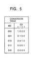
- a drive data conversion circuit 3 converts multiple grayscale pixel data MD into 4-bit pixel drive data GD in accordance with a data conversion table shown in Fig. 5 and supplies the four-bit pixel drive data GD to a memory 4.
- the memory 4 sequentially captures and stores the 4-bit pixel drive data GD. Each time the memory 4 finishes the writing of one image-frame (n rows ⁇ m columns) of pixel drive data GD 1,1 to GD n,m , the memory 4 divides the pixel drive data GD 1,1 to GD n,m into bit digits (Oth to 3rd bits) and reads one display line's worth of this data at a time in correspondence with the subfields SF0 to SF3 respectively. The memory 4 supplies m pixel drive data bits corresponding to one display line to a column electrode driver circuit 5 as the pixel drive data bits DB1 to DBm.
- the memory 4 reads only the 0th bit of each of the pixel drive data GD 1,1 to GD n,m one display line at a time, and supplies the respective 0th bits to the column electrode driver circuit 5 as the pixel drive data bits DB1 to DBm.
- the memory 4 reads, one display line at a time, only the respective first bits of pixel drive data GD 1,1 to GD n,m and supplies these first bits to the column electrode driver circuit 5 as the pixel drive data bits DB1 to DBm.
- the memory 4 reads only the respective second bits of the pixel drive data GD 1,1 to GD n,m one display line at a time and supplies these second bits to the column electrode driver circuit 5 as pixel drive data bits DB1 to DBm. Subsequently, in the subfield SF3, the memory 4 reads only the respective third bits of the pixel drive data GD 1,1 to GD n,m one display line at a time and supplies these third bits to the column electrode driver circuit 5 as pixel drive data bits DB1 to DBm.
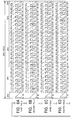
- a drive control circuit 6 generates various timing signals for grayscale-driving the PDP 100 in accordance with the light emission drive sequences shown in the following drawings:
- the drive control circuit 6 supplies these timing signals to the column electrode driver circuit 5, the row electrode Y driver circuit 7 and the row electrode X driver circuit 8 respectively.
- a series of driving shown in Figs. 6A to 6H is executed repeatedly.
- the column electrode driver circuit 5, the row electrode Y driver circuit 7, and the row electrode X driver circuit 8 generate various drive pulses (not shown) to drive the PDP 100 as described below in accordance with the timing signals supplied by the drive control circuit 6, and apply these drive pulses to the column electrodes D 1 to D m , row electrodes X 1 to X n , and row electrodes Y 1 to Y n of the PDP 100, respectively.
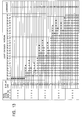
- each of the fields of the video input signal is constituted by the five subfields SF0 to SF4.
- the leading subfield SF0 sequentially executes a reset step R and an address step W0.
- the reset step R causes all the discharge cells G (1,1) to G (n,m) of the PDP 100 to perform a reset discharge all together and initializes the discharge cells G (1,1) to G (n,m) in a lit mode (state in which a wall charge of a predetermined amount is formed).
- the discharge cells G arranged on the first to nth display lines of the PDP 100 are selectively made to perform an erase discharge in accordance with the pixel drive data GD as shown in Fig. 5, in sequence one display line at a time, so that the selected discharge cells are brought into an unlit mode (state where the wall charge has been erased or extinguished).
- the discharge cells in which the erasure discharge is not induced in this address step W0 retain the state up until immediately before this address step W0, that is, the lit mode.
- Each of the subfields SF1 to SF3 are further divided into eight subfields SF1 1 to SF1 8 , SF2 1 to SF2 8 , and SF3 1 to SF3 8 respectively.
- Address steps W1 to W8 are executed in the subfields SF1 1 to SF1 8 , SF2 1 to SF2 8 , and SF3 1 to SF3 8 respectively.
- the subfield SF1 (SF2, SF3) may be referred to as a primary subfield and the subfield SF1 i (SF2 i , SF3 i ) may be referred to as a secondary subfield.
- the address step W1 only discharge cells that are arranged in the (8N-7)th display lines (i.e. , the 1st, 9th, 17th, ..., and (n-7)th display lines) among all the discharge cells G (1,1) to G (n,m) in the PDP 100, are selectively caused to perform an erasure discharge in accordance with the pixel drive data.
- discharge cells in which an erasure discharge is induced are set to the unlit mode, and discharge cells in which an erasure discharge is not induced retain the state up until immediately before the address step W1. That is, the address step W1 sets the discharge cells arranged on the (8N-7)th display lines to either the unlit or lit mode in accordance with the pixel drive data.
- the address step W2 only the discharge cells arranged on the (8N-6)th display lines (i.e., the 2nd, 10th, 18th, ..., and (n-6)th display lines) are selectively made to perform an erasure discharge in accordance with the pixel drive data.
- discharge cells in which an erasure discharge is induced are set to the unlit mode, and discharge cells in which an erasure discharge is not induced retain the state up until immediately before the address step W2. That is, the address step W2 sets the discharge cells arranged on the (8N-6)th display lines to either the unlit mode or the lit mode in accordance with the pixel drive data.
- the address step W3 only discharge cells arranged on the (8N-5)th display lines (i.e., the 3rd, 11th, 19th, ..., and (n-5)th display lines) are selectively made to perform an erasure discharge in accordance with the pixel drive data.
- discharge cells in which an erasure discharge is induced are set to the unlit mode, and discharge cells in which an erasure discharge is not induced retain the state up until directly before the address step W3. That is, the address step W3 sets the discharge cells arranged on the (8N-5)th display lines to either the unlit or lit mode in accordance with the pixel drive data.
- the address step W4 only discharge cells arranged on the (8N-4)th display lines (i.e., the 4th, 12th, 20th, ..., and (n-4)th display lines) are selectively made to perform an erasure discharge in accordance with the pixel drive data.
- discharge cells in which an erasure discharge is induced are set to the unlit mode, and discharge cells in which an erasure discharge is not induced retain the state up until directly before the address step W4. That is, the address step W4 sets the discharge cells arranged on the (8N-4)th display lines to either the unlit or lit mode in accordance with the pixel drive data.
- the address step W5 only discharge cells arranged on the (8N-3)th display lines (i.e., the 5th, 13th, 21st, ..., and (n-3)th display lines) are selectively made to perform an erasure discharge in accordance with the pixel drive data.
- discharge cells in which an erasure discharge is induced are set to the unlit mode, and discharge cells in which an erasure discharge is not induced retain the state up until directly before the address step W5. That is, the address step W5 sets the discharge cells arranged on the (8N-3)th display lines to either the unlit or lit mode in accordance with the pixel drive data.
- the address step W6 only discharge cells arranged on the (8N-2)th display lines (i.e., the 6th, 14th, 22nd,... , and (n-2)th display lines) are selectively made to perform an erasure discharge in accordance with the pixel drive data.
- discharge cells in which an erasure discharge is induced are set to the unlit mode, and discharge cells in which an erasure discharge is not induced retain the state up until directly before the address step W6. That is, the address step W6 sets the discharge cells arranged on the (8N-2)th display lines to either the unlit or lit mode in accordance with the pixel drive data.
- the address step W7 only discharge cells arranged on the (8N-1)th display lines (i.e., the 7th, 15th, 23rd, ..., and (n-1)th display lines) are selectively made to perform an erasure discharge in accordance with the pixel drive data. Discharge cells in which an erasure discharge is induced are set to the unlit mode, and discharge cells in which an erasure discharge is not induced retain the state up until directly before the address step W7. That is, the address step W7 sets the discharge cells arranged on the (8N-1)th display lines to either the unlit or lit mode in accordance with the pixel drive data.
- the address step W8 only discharge cells arranged on the (8N)th display lines (i.e., the 8th, 16th, 24th, ..., and nth display lines) are selectively made to perform an erasure discharge in accordance with the pixel drive data. Discharge cells in which an erasure discharge is induced are set to the unlit mode, and discharge cells in which an erasure discharge is not induced retain the state up until directly before the address step W8. That is, the address step W8 sets the discharge cells arranged on the (8N)th display lines to either the unlit or lit mode in accordance with the pixel drive data.
- a sustain step I which causes only the discharge cells set to the lit mode to discharge light continuously over the period '1', is executed.
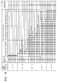
- the drive control circuit 6 performs light emission driving as shown in Figs. 7 to 14 in accordance with the light emission drive sequences shown in Figs. 6A to 6H.
- a light emission display based on first grayscale driving is executed. Because the 0th bit of the pixel drive data GD is logic level 1, an erasure discharge (indicated by the black circles) is induced in the discharge cells in the address step W0 of the subfield SF0, and the discharge cells become the unlit mode.
- the driving scheme shown in Figs. 6A to 6H the opportunity, in a single field display period, for discharge cells to shift from the unlit mode to the lit mode arises only in the reset step R of the leading subfield SF0. Accordingly, discharge cells that have become the unlit mode retain the unlit state in the course of the single field display period.
- each discharge cell retains an unlit state in the course of a single field display period, thereby achieving the luminance level (brightness level) 0 as shown in Fig. 15.
- a light emission display based on second grayscale driving is implemented. Because the first bit of the pixel drive data GD is logic level 1, an erasure discharge (indicated by overlapping circles) is induced in the discharge cells in the address steps W1 to W8 of the subfield SF1. Thereupon, because discharge cells are initialized in the lit mode in the reset step R of the leading subfield SF0, sustained discharge light emission is implemented continuously in the sustain steps I that exist in the interval up until the erasure discharge is induced. For example, in the light emission drive sequence shown in Fig. 6A, the address steps are executed as follows:
- the discharge cells perform a sustained discharge continuously in the sustain steps I of the following subfields:
- the discharge cells arranged on each display line are each driven at a luminance level corresponding with the period of the light emission produced by the sustained discharge induced in the course of a single field display period, as shown in Fig. 15.
- the discharge cells arranged on the (8N-7)th display line are at the luminance level '8'; the discharge cells arranged on the (8N-6)th display lines are at the luminance level '5'; the discharge cells arranged on the (8N-5)th display lines are at the luminance level '2'; the discharge cells arranged on the (8N-4)th display lines are at the luminance level '7'; the discharge cells arranged on the (8N-3)th display lines are at the luminance level '4'; the discharge cells arranged on the (8N-2)th display lines are at the luminance level '1'; the discharge cells arranged on the (8N-1)th display lines are at the luminance level '6'; and the discharge cells arranged on the (8N)th display lines are at the luminance level '3'.
- a light emission display based on third grayscale driving is performed. Because the second bit of the pixel drive data GD is logic level 1, an erasure discharge (indicated by overlapping circles) is induced in each discharge cell in the address steps W1 to W8 of the subfield SF2.
- the discharge cells are initialized in the lit mode in the reset step R of the leading subfield SF0, so that sustained discharge light emission is executed continuously in the sustain steps I that exist during the interval up until the erasure discharge is induced.
- the address steps are executed as follows:
- the discharge cells perform a sustained discharge continuously in the sustain steps I of the following subfields:
- the discharge cells arranged on each display line are each driven at a luminance level corresponding with the period of the light emission produced by the sustained discharge induced in the course of a single field display period, as shown in Fig. 15.
- the discharge cells arranged on the (8N-7)th display lines are at the luminance level '16'; the discharge cells arranged on the (8N-6)th display lines are at the luminance level '13'; the discharge cells arranged on the (8N-5)th display lines are at the luminance level '10'; the discharge cells arranged on the (8N-4)th display lines are at the luminance level '15'; the discharge cells arranged on the (8N-3)th display lines are at the luminance level '12'; the discharge cells arranged on the (8N-2)th display lines are at the luminance level '9'; the discharge cells arranged on the (8N-1)th display lines are at the luminance level '14'; and the discharge cells arranged on the (8N)th display lines are at the luminance level '11'.
- a light emission display based on fourth grayscale driving is performed as detailed below. Because the third bit of the pixel drive data GD is logic level 1, an erasure discharge (indicated by overlapping circles) is induced in each discharge cell in the address steps W1 to W8 of the subfield SF3.
- the discharge cells are initialized in the lit mode in the reset step R of the leading subfield SF0, so that sustained discharge light emission is executed continuously in the sustain steps I that exist during the interval up until the erasure discharge is induced.
- the address steps are executed as follows:
- the discharge cells perform a sustained discharge continuously in the sustain steps I of the following subfields.
- Subfields SF1 1 to SF2 8 and the subfields SF3 1 to SF3 8 for the (8N-7)th display line Subfields SF1 1 to SF2 8 and the subfields SF3 1 to SF3 5 for the (8N-6)th display line; Subfields SF1 1 to SF2 8 and the subfields SF3 1 to SF3 2 for the (8N-5)th display line; Subfields SF1 1 to SF2 8 and the subfields SF3 1 to SF3 7 for the (8N-4)th display line; Subfields SF1 1 to SF2 8 and the subfields SF3 1 to SF3 4 for the (8N-3)th display line; Subfields SF1 1 to SF2 8 and the subfield SF3 1 for the (8N-2)th display line; Subfields SF1 1 to SF2 8 and the subfield SF3 1 for the
- the discharge cells each emit light at a luminance level corresponding with the period of the light emission produced by the sustained discharge induced in the course of a single field display period, as shown in Fig. 15.
- the discharge cells arranged on the (8N-7)th display lines are at the luminance level '24'; the discharge cells arranged on the (8N-6)th display lines are at the luminance level '21'; the discharge cells arranged on the (8N-5)th display lines are at the luminance level '18'; the discharge cells arranged on the (8N-4)th display lines are at the luminance level '23'; the discharge cells arranged on the (8N-3)th display lines are at the luminance level '20'; the discharge cells arranged on the (8N-2)th display lines are at the luminance level '17'; the discharge cells arranged on the (8N-1)th display lines are at the luminance level '22'; and the discharge cells arranged on the (8N)th display lines are at the luminance level '19'.
- a light emission display based on the fifth grayscale driving is implemented. Because all the bits of the pixel drive data GD are logic level 0, erasure discharge is not induced at all during the single field display period. Accordingly, the discharge cells discharge light continuously in the sustain steps I of the subfields SF1 1 to SF1 8 , SF2 1 to SF2 8 , SF3 1 to SF3 8 , and SF4.
- the discharge cells each emit light at a luminance level corresponding with the period of the light emission produced by the sustained discharge induced in the course of a single field display period as shown in Fig. 15.
- the discharge cells arranged on the (8N-7)th display lines are at the luminance level '25'; the discharge cells arranged on the (8N-6)th display lines are at the luminance level '25'; the discharge cells arranged on the (8N-5)th display lines are at the luminance level '25'; the discharge cells arranged on the (8N-4)th display lines are at the luminance level '25'; the discharge cells arranged on the (8N-3)th display lines are at the luminance level '25'; the discharge cells arranged on the (8N-2)th display lines are at the luminance level '25'; the discharge cells arranged on the (8N-1)th display lines are at the luminance level '25'; and the discharge cells arranged on the (8N)th display lines are at the luminance level '25'.
- the first to fifth grayscale driving that is capable of representing luminance corresponding to five levels is executed in accordance with five different pixel drive data GD, namely, '1000', '0100', '0010', '0001', and '0000'.
- different luminance weightings are applied to eight adjacent display lines, and the eight adjacent display lines are driven at different luminance levels determined by the respective luminance weightings, in each of the first to fifth grayscale driving.
- luminance weightings ('1' to '8') are allocated to the eight adjacent display lines in the driving according to the light emission drive sequence for the first field shown in Fig. 6A:
- the line dither offset value generation circuit 21 adds the line dither offset values LD shown in Fig. 4A to the pixel data PD of the display lines, respectively, as shown in Fig. 16.
- the line dither offset values LD As a result of this addition of the line dither offset values LD, the following line-offset-added pixel data LF are obtained for each of the display lines, as shown in Fig. 16.
- (8N-7)th display line the value LF is '010100'; (8N-6)th display line: the value LF is '010111'; (8N-5)th display line: the value LF is '011010'; (8N-4)th display line: the value LF is '010101'; (8N-3)th display line: the value LF is '011000'; (8N-2)th display line: the value LF is '011011'; (8N-1)th display line: the value LF is '010110'; and (8N)th display line: the value LF is '011001'.
- the lower bit discard circuit 23 discards the lower 3 bits of each of these line-offset-added pixel data LF, thereby obtaining the remaining upper 3 bits of data as the multiple grayscale pixel data MD. That is, as shown in Fig. 16, the following multiple grayscale pixel data MD are obtained for the eight adjacent display lines:
- These multiple grayscale pixel data MD are converted into 4-bit pixel drive data GD by the drive data conversion circuit 3.
- the plasma display device shown in Fig. 3 drives each of the eight adjacent display lines to emit light such that the different line dither offset values LD are added to pixel data PD of the display lines and the different luminance weightings are applied to the display lines.
- so-called line dither processing which allows the luminance difference between adjacent display lines to be generated, is implemented.
- the bias of the luminance difference between adjacent display lines of the PDP 100 should be substantially uniform. To this end, the bias is limited to lie within a predetermined value in this embodiment. For example, when '010100' pixel data PD is supplied, the bias of the luminance difference is '2', as shown in Fig. 16.
- the luminance difference between the (8N-7)th and (8N-6)th display lines is '3'; the luminance difference between the (8N-6)th and (8N-5)th display lines is '5'; the luminance difference between the (8N-5)th and (8N-4)th display lines is '3'; the luminance difference between the (8N-4)th and (8N-3)th display lines is '5'; the luminance difference between the (8N-3)th and (8N-2)th display lines is '3'; the luminance difference between the (8N-2)th and (8N-1)th display lines is '3'; and the luminance difference between the (8N-1)th and (8N)th display lines is '5'.
- the bias of the luminance difference between the adjacent display lines is equal to or less than '2' in this embodiment.
- the discharge cells arranged on the (8N-7)th display line are driven to emit light at the luminance level '16' by means of the third grayscale driving
- the discharge cells arranged on the (8N-6)th display line are driven to emit light at the luminance level '13' by means of the third grayscale driving, or are driven to emit light at the luminance level '21' by means of the fourth grayscale driving.
- the bias of the luminance differences between adjacent display lines is restricted in a predetermined range, so that a high quality dither-processed image with a smaller luminance bias is expressed.
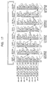
- the first to eighth fields of the video input signal constitute one cycle, and the weighting of the line dither processing for each of the eight adjacent display lines is changed for each field as shown in Fig. 17.
- the first to eighth line dither processes are allocated to the display lines as follows:
- the first to eighth line dither processes are allocated to the display lines as follows:
- the first to eighth line dither processes are allocated to the display lines as follows:
- the first to eighth line dither processes are allocated to the display lines as follows:
- the first to eighth line dither processes are allocated to the display lines as follows:
- the first to eighth line dither processes are allocated to the display lines as follows:
- the first to eighth line dither processes are allocated to the display lines as follows:
- the first to eighth line dither processes are allocated to the display lines as follows:
- the respective line dither processing is applied alternately to upper and lower display in the screen for each field.
- the fifth line dither processing which adds a '4' line dither offset value LD to the pixel data PD and performs light emission driving corresponding with a '4' luminance weighting, is allocated to the (8N-3)th display line in the first field.
- the fifth line dither processing is performed on the (8N-7)th display line located below the (8N-3)th display line in the screen as indicated by the arrow.
- the fifth line dither processing is performed on the (8N-1)th display line located above the (8N-7)th display line as shown by the arrow.
- the fifth line dither processing is performed on the (8N-5)th display line located below the (8N-1)th display line as indicated by the arrow.
- the fifth line dither processing is performed on the (8N-6)th display line located above the (8N-5)th display line as indicated by the arrow.
- the fifth line dither processing is performed on the (8N-2)th display line located below the (8N-6)th display line as indicated by the arrow.
- the fifth line dither processing is performed on the (8N-4)th display line located above the (8N-2)th display line as indicated by the arrow.
- the fifth line dither processing is performed on the (8N)th display line located below the (8N-4)th display line as indicated by the arrow.
- the luminance weighting is the same in each of the subfields SF1 to SF4, that is, the whole light emission period in each sustain step I of each of the subfields SF1 1 to SF1 8 , SF2 1 to SF2 8 , SF3 1 to SF3 8 , and SF4 is '1', the weighting for each subfield may be different.
- a light emission drive sequence as shown in Fig. 18 may be adopted, in which the weighting of the subfields SF1 to SF4 are as follows:
- the light emission period in the sustain step I of each of the subfields SF1 1 to SF1 8 is '1'
- the light emission period in the sustain step I of each of the subfields SF2 1 to SF2 8 is '2'
- the light emission period in the sustain step I of each of the subfields SF3 1 to SF3 8 is '3'
- the light emission period in the sustain step I of the subfield SF4 is '4'.
- Fig. 19 shows light emission drive patterns based on the light emission drive sequence shown in Fig. 18.
- the discharge cells retain the unlit state in the course of the single field display period and driving at the luminance level 0 is performed.
- the discharge cells are driven at the following luminance levels:
- the discharge cells are driven at the following luminance levels:
- the discharge cells are driven at the following luminance levels:
- the flicker cycle is the same as the vertical synchronization frequency of the video input signal. Therefore, when a PAL-system television signal with a low vertical synchronization frequency, or similar, is supplied as the video input signal, flicker is more prominent.
- the light emission drive sequence shown in Fig. 21 is adopted in place of the light emission drive sequence shown in Fig. 18.
- the light emission drive sequence shown in Fig. 21 uses the following luminance weightings for the subfields SF1, SF2, SF3, and SF4:
- subfields SF1 to SF3 are each divided into eight subfields SF1 1 to SF1 8 , SF2 1 to SF2 8 , and SF3 1 to SF3 8 .
- a reset step R which initializes all the discharge cells in the lit mode
- an address step W0 which causes the selected discharge cells to make the transition to the unlit mode by causing these cells to selectively perform an erasure discharge in accordance with pixel drive data GD, in sequence one display line at a time, are executed in the leading subfield SF01.
- the subfields SF1 1 to SF1 8 are executed as detailed below.
- the sustain step I in which the discharge cells set to the lit mode are made to repeatedly perform a sustained discharge over period '1', and the address step W6, in which only the discharge cells arranged on the (8N-2)th display line are made to selectively perform an erasure discharge in accordance with pixel drive data GD, are executed in the leading subfield SF1 1 of the subfield SF1.
- the sustain step I in which the discharge cells set to the lit mode are made to repeatedly perform a sustained discharge over period '1', and the address step W3, in which only the discharge cells arranged on the (8N-5)th display line are made to selectively perform an erasure discharge in accordance with pixel drive data GD, are executed.
- the sustain step I in which the discharge cells set to the lit mode are made to repeatedly perform a sustained discharge over period '1', and the address step W8, in which only the discharge cells arranged on the (8N)th display line are made to selectively perform an erasure discharge in accordance with pixel drive data GD, are executed.
- the sustain step I in which the discharge cells set to the lit mode are made to repeatedly perform a sustained discharge over period '1', and the address step W5, in which only the discharge cells arranged on the (8N-3)th display line are made to selectively perform an erasure discharge in accordance with pixel drive data GD, are executed.
- the sustain step I in which the discharge cells set to the lit mode are made to repeatedly perform a sustained discharge over period '1', and the address step W2, in which only the discharge cells arranged on the (8N-6)th display line are made to selectively perform an erasure discharge in accordance with pixel drive data GD, are executed.
- the sustain step I in which the discharge cells set to the lit mode are made to repeatedly perform a sustained discharge over period '1', and the address step W7, in which only the discharge cells arranged on the (8N-1)th display line are made to selectively perform an erasure discharge in accordance with pixel drive data GD, are executed.
- the sustain step I in which the discharge cells set to the lit mode are made to repeatedly perform a sustained discharge over period '1', and the address step W4, in which only the discharge cells arranged on the (8N-4)th display line are made to selectively perform an erasure discharge in accordance with pixel drive data GD, are executed.
- the sustain step I in which the discharge cells set to the lit mode are made to repeatedly perform a sustained discharge over period '1', and the address step W1, in which only the discharge cells arranged on the (8N-7)th display line are made to selectively perform an erasure discharge in accordance with pixel drive data GD, are executed.
- the subfield SF3 is executed as described below.
- the sustain step I in which the discharge cells set to the lit mode are made to repeatedly perform a sustained discharge over period '10', and the address step W6, in which only the discharge cells arranged on the (8N-2)th display line are made to selectively perform an erasure discharge in accordance with pixel drive data GD, are executed in the leading subfield SF3 1 of the subfield SF3.
- the next subfield i.e.
- subfield SF3 2 subfield SF3 2
- the sustain step I in which the discharge cells set to the lit mode are made to repeatedly perform a sustained discharge over period '2'
- the address step W3 in which only the discharge cells arranged on the (8N-5)th display line are made to selectively perform an erasure discharge in accordance with pixel drive data GD, are executed.
- the sustain step I in which the discharge cells set to the lit mode are made to repeatedly perform a sustained discharge over period '2', and the address step W8, in which only the discharge cells arranged on the (8N)th display line are made to selectively perform an erasure discharge in accordance with pixel drive data GD, are executed.
- the sustain step I in which the discharge cells set to the lit mode are made to repeatedly perform a sustained discharge over period '2', and the address step W5, in which only the discharge cells arranged on the (8N-3)th display line are made to selectively perform an erasure discharge in accordance with pixel drive data GD, are executed.
- the sustain step I in which the discharge cells set to the lit mode are made to repeatedly perform a sustained discharge over period '2', and the address step W2, in which only the discharge cells arranged on the (8N-6)th display line are made to selectively perform an erasure discharge in accordance with pixel drive data GD, are executed.
- the sustain step I in which the discharge cells set to the lit mode are made to repeatedly perform a sustained discharge over period '2', and the address step W7, in which only the discharge cells arranged on the (8N-1)th display line are made to selectively perform an erasure discharge in accordance with pixel drive data GD, are executed.
- the sustain step I in which the discharge cells set to the lit mode are made to repeatedly perform a sustained discharge over period '2', and the address step W4, in which only the discharge cells arranged on the (8N-4)th display line are made to selectively perform an erasure discharge in accordance with pixel drive data GD, are executed.
- the sustain step I in which the discharge cells set to the lit mode are made to repeatedly perform a sustained discharge over period '2', and the address step W1, in which only the discharge cells arranged on the (8N-7)th display line are made to selectively perform an erasure discharge in accordance with pixel drive data GD, are executed.
- the subfield SF02 is executed.
- the reset step R which initializes all the discharge cells in the lit mode
- an address step W0 which causes selected discharge cells to make the transition to the unlit mode by causing these cells to selectively perform an erasure discharge in accordance with pixel drive data GD, in sequence one display line at a time, are executed in the subfield SF02.
- the subfield SF2 is executed as detailed below.
- the sustain step I in which the discharge cells set to the lit mode are made to repeatedly perform a sustained discharge over period '9', and the address step W6, in which only the discharge cells arranged on the (8N-2)th display line are made to selectively perform an erasure discharge in accordance with pixel drive data GD, are executed in the leading subfield SF2 1 of the subfield SF2.
- the sustain step I in which the discharge cells set to the lit mode are made to repeatedly perform a sustained discharge over period '1', and the address step W3, in which only the discharge cells arranged on the (8N-5)th display line are made to selectively perform an erasure discharge in accordance with pixel drive data GD, are executed.
- the sustain step I in which the discharge cells set to the lit mode are made to repeatedly perform a sustained discharge over period '1', and the address step W8, in which only the discharge cells arranged on the (8N)th display line are made to selectively perform an erasure discharge in accordance with pixel drive data GD, are executed.
- the sustain step I in which the discharge cells set to the lit mode are made to repeatedly perform a sustained discharge over period '1', and the address step W5, in which only the discharge cells arranged on the (8N-3)th display line are made to selectively perform an erasure discharge in accordance with pixel drive data GD, are executed.
- the sustain step I in which the discharge cells set to the lit mode are made to repeatedly perform a sustained discharge over period '1', and the address step W2, in which only the discharge cells arranged on the (8N-6)th display line are made to selectively perform an erasure discharge in accordance with pixel drive data GD, are executed.
- the sustain step I in which the discharge cells set to the lit mode are made to repeatedly perform a sustained discharge over period '1', and the address step W7, in which only the discharge cells arranged on the (8N-1)th display line are made to selectively perform an erasure discharge in accordance with pixel drive data GD, are executed.
- the sustain step I in which the discharge cells set to the lit mode are made to repeatedly perform a sustained discharge over period '1', and the address step W4, in which only the discharge cells arranged on the (8N-4)th display line are made to selectively perform an erasure discharge in accordance with pixel drive data GD, are executed.
- the sustain step I in which the discharge cells set to the lit mode are made to repeatedly perform a sustained discharge over period '1', and the address step W1, in which only the discharge cells arranged on the (8N-7)th display line are made to selectively perform an erasure discharge in accordance with pixel drive data GD, are executed.
- the subfield SF4 is executed.
- the sustain step I in which the discharge cells set to the lit mode are made to repeatedly perform a sustained discharge over period '4', is implemented.
- the reset step R which initializes all the discharge cells in the lit mode is executed twice, namely, at the start of the first half of the single field display period and at the start of the second half of this period.
- the driving operations equivalent to the subfields SF1 and SF3 shown in Fig. 18 are executed in the first half of the single field display period, while the driving operations equivalent to the subfields SF2 and SF4 are executed in the second half.
- Fig. 22 shows the pixel drive data GD and light emission drive pattern based on the light emission drive sequence shown in Fig. 21.
- a light emission display based on the first grayscale driving is performed as detailed below. That is, as shown in Fig. 22, an erasure discharge (indicated by a black circle) is induced in each of the discharge cells in the address step W0 of each of the subfields SF01 and 02.
- the opportunity to set the discharge cells to the lit mode arises only twice in the course of the single field display period, namely, in the reset step R of the subfield SF01 and in the reset step R of the subfield SF02. Therefore, in the first grayscale driving according to the '1000' pixel drive data GD, a light emission display at the luminance level 0 is executed as a result of the discharge cells retaining the unlit mode in the course of the single field display period.
- a light emission display based on second grayscale driving is performed as detailed below. That is, as shown in Fig. 22, an erasure discharge (indicated by overlapping circles) is induced in each of the discharge cells in the address steps W1 to W8 of the subfield SF1, and an erasure discharge (indicated by a black circle) is induced in each of the discharge cells in the address step W0 of the subfield SF02.
- the discharge cells arranged on each display line are each driven to emit light at a luminance level that corresponds with the period of the light emission generated by the sustained discharge induced during the single field display period, that is, the discharge cells arranged on the (8N-7)th display line are at the luminance level '8'; the discharge cells arranged on the (8N-6)th display line are at the luminance level '5'; the discharge cells arranged on the (8N-5)th display line are at the luminance level '2'; the discharge cells arranged on the (8N-4)th display line are at the luminance level '7'; the discharge cells arranged on the (8N-3)th display line are at the luminance level '
- a light emission display based on third grayscale driving is performed as detailed below. That is, as shown in Fig. 22, an erasure discharge (indicated by overlapping circles) is first induced in each of the discharge cells in the address steps W1 to W8 of the subfield SF1. Because the discharge cells are initialized in the lit mode in the reset step R of the leading subfield SF01, sustained discharge light emission (indicated by a white circle) is performed continuously in sustain steps I that exist during the interval up until the erasure discharge is induced.
- the discharge cells arranged on each display line are driven to emit light at a luminance level that corresponds with the total period of the light emission generated by the sustained discharge induced in the sustain step I of each of the subfields SF1 and SF2 during the single field display period, that is, the discharge cells arranged on the (8N-7)th display line are at the luminance level '24'; the discharge cells arranged on the (8N-6)th display line are at the luminance level '18'; the discharge cells arranged on the (8N-5)th display line are at the luminance level '12'; the discharge cells arranged on the (8N-4)th display line are at the luminance level '22'; the discharge cells arranged on the (8N-3)th display line are at the luminance level '16'; the discharge cells arranged on the (8N-2)th display line are at the luminance level '10'; the discharge cells arranged on the (8N-1)th display
- a light emission display based on fourth grayscale driving is performed as detailed below. That is, as shown in Fig. 22, an erasure discharge (indicated by overlapping circles) is first induced in each of the discharge cells in the address steps W1 to W8 of the subfield SF3. Because the discharge cells are initialized in the lit mode in the reset step R of the leading subfield SF01, sustained discharge light emission (indicated by a white circle) is performed continuously in sustain steps I that exist during the interval up until the erasure discharge is induced.
- sustained discharge light emission is performed over period '1' in the sustain step I of each of the subfields SF1 1 to SF1 8 , and SF2 2 to SF2 8 , over period '9' in the sustain step I of the subfield SF2 1 , over period '10' in the sustain step I of the subfield SF3 1 , and over period '2' in the sustain step I of each of the subfields SF3 2 to SF3 8 .
- a light emission display based on the fifth grayscale driving is performed as detailed below.
- the fifth grayscale driving erasure discharge is not induced at all during the single field display period as shown in Fig. 22, so that the discharge cells discharge light continuously in the sustain steps I of each of the subfields SF1 1 to SF1 8 , SF2 1 to SF2 8 , SF3 1 to SF3 8 , and SF4. Therefore, the discharge cells arranged on each display line are driven to emit light at the luminance level '52'.
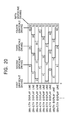
- the driving shown in Figs. 21 and 22 performs the light emission driving on the discharge cells arranged on eight adjacent display lines at five luminance levels as shown in Fig. 20.
- the driving shown in Figs. 21 and 22 when the discharge cells are caused to emit light (sustained discharge) continuously over a period determined by the pixel drive data in a single field display period, the driving is executed with dispersion by means of a first-half subfield group (SF1 1 to SF1 8 and SF3 1 to SF3 8 ) and a second-half subfield group (SF2 1 to SF2 8 and SF4). Accordingly, as shown in Fig. 22, there are two opportunities for the discharge cells to make the transition from the lit state to the unlit state within the single field display period in each of the third and fourth grayscale driving.
- the frequency with which the discharge cells switch from the lit state to the unlit state is two times the vertical synchronization frequency, so that a favorable display is provided in which flicker is suppressed even when a PAL-system television signal with a low vertical synchronization frequency, or similar, is supplied as the video input signal.
- the light emission period is allocated to the sustain step I of each subfield such that the luminance levels of the eight adjacent display lines are the same as those shown in Fig. 20 even when the discharge cells are driven to emit light by means of dispersion into two, namely with a first-half subfield group and a second-half subfield group.
- the light emission periods are set as follows:
- the light emission period in the leading subfield SF2 1 (SF3 1 ) of the lower subfields SF2 1 to SF2 8 (SF3 1 to SF3 8 ) in the subfield SF2 (SF3) is set larger than the light emission period in subsequent subfields SF2 2 to SF2 8 (SF3 2 to SF3 8 ).
- so-called selective erasure addressing is adopted in order to set each of the discharge cells to either the lit mode or unlit mode in accordance with the pixel data. Specifically, all the discharge cells are preset to the lit mode and the selected discharge cells are made to make the transition to the unlit mode in accordance with pixel data.
- the present invention can be similarly applied when so-called selective write addressing is adopted.
- the selective write addressing all the discharge cells are preset to the unlit mode and a write discharge is induced in the selected discharge cells in accordance with pixel data so that these discharge cells make the transition to the lit mode.
- Fig. 23 shows a light emission drive sequence for a case where a light emission drive sequence as shown in Fig. 21 is implemented with the selective write addressing.
- Fig. 24 shows light emission drive patterns that are executed based on the light emission drive sequence shown in Fig. 23.
- the drive data conversion circuit 3 shown in Fig. 3 converts multiple grayscale pixel data MD into 5-bit pixel drive data GD consisting of 0th to 4th bits in accordance with the data conversion table shown in Fig. 30.
- the drive control circuit 6 implements light emission drive control on the basis of the light emission drive sequence as shown in Fig. 23 in accordance with this pixel drive data GD.
- the subfields SF0, SF3 1 to SF3 8 , SF2 1 to SF2 8 , SF1 1 to SF1 8 , SF4, and SF2 1 to SF2 8 are executed in sequence.
- the reset step R which initializes each of the discharge cells in the unlit mode by inducing a reset discharge in all the discharge cells to form a wall charge in each discharge cell
- the address step W0 which sets the selected discharge cells in the lit mode by causing the write discharge in the selected discharge cells in accordance with the 0th bit of the pixel drive data GD, are executed in the subfield SF0.
- the subfield SF3 is executed as follows.
- the address step W1 in which only the discharge cells arranged on the (8N-7)th display line are made to selectively perform a write discharge in accordance with the third bit of the pixel drive data GD and then set to the lit mode, and a sustain step I, in which the discharge cells set to the lit mode are made to repeatedly perform a sustained discharge over period '2', are executed.
- the address step W4 in which only the discharge cells arranged on the (8N-4)th display line are made to selectively perform a write discharge in accordance with the third bit of the pixel drive data GD and then set to the lit mode, and a sustain step I, in which the discharge cells set to the lit mode are made to repeatedly perform a sustained discharge over period '2', are executed.
- the address step W7 in which only the discharge cells arranged on the (8N-1)th display line are made to selectively perform a write discharge in accordance with the third bit of the pixel drive data GD and then set to the lit mode, and a sustain step I, in which the discharge cells set to the lit mode are made to repeatedly perform a sustained discharge over period '2', are executed.
- the address step W2 in which only the discharge cells arranged on the (8N-6)th display line are made to selectively perform a write discharge in accordance with the third bit of the pixel drive data GD and then set to the lit mode, and a sustain step I, in which the discharge cells set to the lit mode are made to repeatedly perform a sustained discharge over period '2', are executed.
- the address step W5 in which only the discharge cells arranged on the (8N-3)th display line are made to selectively perform a write discharge in accordance with the third bit of the pixel drive data GD and then set to the lit mode, and a sustain step I, in which the discharge cells set to the lit mode are made to repeatedly perform a sustained discharge over period '2', are executed.
- the address step W8 in which only the discharge cells arranged on the (8N)th display line are made to selectively perform a write discharge in accordance with the third bit of the pixel drive data GD and then set to the lit mode, and a sustain step I, in which the discharge cells set to the lit mode are made to repeatedly perform a sustained discharge over period '2', are executed.
- the address step W3 in which only the discharge cells arranged on the (8N-5)th display line are made to selectively perform a write discharge in accordance with the third bit of the pixel drive data GD and then set to the lit mode, and a sustain step I, in which the discharge cells set to the lit mode are made to repeatedly perform a sustained discharge over period '2', are executed.
- the address step W3 in which only the discharge cells arranged on the (8N-2)th display line are made to selectively perform a write discharge in accordance with the third bit of the pixel drive data GD and then set to the lit mode, and a sustain step I, in which the discharge cells set to the lit mode are made to repeatedly perform a sustained discharge over period '10', are executed.
- the subfield SF1 is executed as follows.
- the address step W1 in which only the discharge cells arranged on the (8N-7)th display line are made to selectively perform a write discharge in accordance with the first bit of the pixel drive data GD and then set to the lit mode, and a sustain step I, in which the discharge cells set to the lit mode are made to repeatedly perform a sustained discharge over period '1', are executed.
- the address step W4 in which only the discharge cells arranged on the (8N-4)th display line are made to selectively perform a write discharge in accordance with the first bit of the pixel drive data GD and then set to the lit mode, and a sustain step I, in which the discharge cells set to the lit mode are made to repeatedly perform a sustained discharge over period '1', are executed.
- the address step W7 in which only the discharge cells arranged on the (8N-1)th display line are made to selectively perform a write discharge in accordance with the first bit of the pixel drive data GD and then set to the lit mode, and a sustain step I, in which the discharge cells set to the lit mode are made to repeatedly perform a sustained discharge over period '1', are executed.
- the address step W2 in which only the discharge cells arranged on the (8N-6)th display line are made to selectively perform a write discharge in accordance with the first bit of the pixel drive data GD and then set to the lit mode, and a sustain step I, in which the discharge cells set to the lit mode are made to repeatedly perform a sustained discharge over period '1', are executed.
- the address step W5 in which only the discharge cells arranged on the (8N-3)th display line are made to selectively perform a write discharge in accordance with the first bit of the pixel drive data GD and then set to the lit mode, and a sustain step I, in which the discharge cells set to the lit mode are made to repeatedly perform a sustained discharge over period '1', are executed.
- the address step W8 in which only the discharge cells arranged on the (8N)th display line are made to selectively perform a write discharge in accordance with the first bit of the pixel drive data GD and then set to the lit mode, and a sustain step I, in which the discharge cells set to the lit mode are made to repeatedly perform a sustained discharge over period '1', are executed.
- the address step W3 in which only the discharge cells arranged on the (8N-5)th display line are made to selectively perform a write discharge in accordance with the first bit of the pixel drive data GD and then set to the lit mode, and a sustain step I, in which the discharge cells set to the lit mode are made to repeatedly perform a sustained discharge over period '1', are executed.
- the address step W3 in which only the discharge cells arranged on the (8N-2)th display line are made to selectively perform a write discharge in accordance with the first bit of the pixel drive data GD and then set to the lit mode, and a sustain step I, in which the discharge cells set to the lit mode are made to repeatedly perform a sustained discharge over period '1', are executed.
- the subfield SF4 is executed as follows.
- a reset step R which initializes all the discharge cells in the unlit mode
- an address step W0 in which selected discharge cells are made to perform a write discharge in accordance with the fourth bit of the pixel drive data GD and then set to the lit mode
- a sustain step I in which the discharge cells set to the lit mode are repeatedly made to perform a sustained discharge over period '4', are executed.
- the subfield SF2 is executed as below.
- the address step W1 in which only the discharge cells arranged on the (8N-7)th display line are made to selectively perform a write discharge in accordance with the second bit of the pixel drive data GD and then set to the lit mode, and a sustain step I, in which the discharge cells set to the lit mode are made to repeatedly perform a sustained discharge over period '1', are executed.
- the address step W4 in which only the discharge cells arranged on the (8N-4)th display line are made to selectively perform a write discharge in accordance with the second bit of the pixel drive data GD and then set to the lit mode, and a sustain step I, in which the discharge cells set to the lit mode are made to repeatedly perform a sustained discharge over period '1', are executed.
- the address step W7 in which only the discharge cells arranged on the (8N-1)th display line are made to selectively perform a write discharge in accordance with the second bit of the pixel drive data GD and then set to the lit mode
- a sustain step I in which the discharge cells set to the lit mode are made to repeatedly perform a sustained discharge over period '1', are executed.
- the address step W2 in which only the discharge cells arranged on the (8N-6)th display line are made to selectively perform a write discharge in accordance with the second bit of the pixel drive data GD and then set to the lit mode, and a sustain step I, in which the discharge cells set to the lit mode are made to repeatedly perform a sustained discharge over period '1', are executed.
- the address step W5 in which only the discharge cells arranged on the (8N-3)th display line are made to selectively perform a write discharge in accordance with the second bit of the pixel drive data GD and then set to the lit mode, and a sustain step I, in which the discharge cells set to the lit mode are made to repeatedly perform a sustained discharge over period '1' , are executed.
- the address step W8 in which only the discharge cells arranged on the (8N)th display line are made to selectively perform a write discharge in accordance with the second bit of the pixel drive data GD and then set to the lit mode, and a sustain step I, in which the discharge cells set to the lit mode are made to repeatedly perform a sustained discharge over period '1', are executed.
- the address step W3 in which only the discharge cells arranged on the (8N-5)th display line are made to selectively perform a write discharge in accordance with the second bit of the pixel drive data GD and then set to the lit mode, and a sustain step I, in which the discharge cells set to the lit mode are made to repeatedly perform a sustained discharge over period '1', are executed.
- the address step W3 in which only the discharge cells arranged on the (8N-2)th display line are made to selectively perform a write discharge in accordance with the second bit of the pixel drive data GD and then set to the lit mode, and a sustain step I, in which the discharge cells set to the lit mode are made to repeatedly perform a sustained discharge over period '9', are executed.
- Whether the write discharge is induced or not in the address steps W0 to W8 of the subfield SF0 is determined by the 0th bit of the pixel drive data GD shown in Fig. 24. Whether the write discharge is induced or not in the address steps W0 to W8 of the subfield SF1 is determined by the first bit of the pixel drive data GD. Whether the write discharge is induced or not in the address steps W0 to W8 of the subfield SF2 is determined by the second bit of the pixel drive data GD. Whether the write discharge is induced or not in the address steps W0 to W8 of the subfield SF3 is determined by the third bit of the pixel drive data GD.
- a light emission display based on the first grayscale driving is performed as detailed below. That is, as shown in Fig. 24, no write discharge (indicated by overlapping circles) is performed during the single field display period, so that a light emission display at the luminance level 0 is executed as a result of the respective discharge cells retaining the unlit mode during the single field display period.
- a light emission display based on the second grayscale driving is performed as detailed below. That is, as shown in Fig. 24, a write discharge (indicated by overlapping circles) is induced in each of the address steps W1 to W8 in only the subfield SF1, so that sustained discharge light emission (indicated by a white circle) is performed continuously in sustain steps I that exist during the interval until the reset step R of the subfield SF4 is implemented after the write discharge is induced.
- the discharge cells arranged on the display lines are each driven to emit light at a luminance level that corresponds with the period of the light emission generated by the sustained discharge that is induced during the single field display period.
- the discharge cells arranged on the (8N-7)th display line are at the luminance level '8'; the discharge cells arranged on the (8N-6)th display line are at the luminance level '5'; the discharge cells arranged on the (8N-5)th display line are at the luminance level '2'; the discharge cells arranged on the (8N-4)th display line are at the luminance level '7'; the discharge cells arranged on the (8N-3)th display line are at the luminance level '4'; the discharge cells arranged on the (8N-2)th display line are at the luminance level '1'; the discharge cells arranged on the (8N-1)th display line are at the luminance level '6'; and the discharge cells arranged on the (8N)th display line are at the luminance level '3'.
- a light emission display based on third grayscale driving is performed as detailed below. That is, as shown in Fig. 24, a write discharge (indicated by overlapping circles) is induced in respective discharge cells in the address steps W1 to W8 of the subfields SF1 and SF2. Accordingly, sustained discharge light emission (indicated by a white circle) is performed continuously in sustain steps I that exist during the interval until the reset step R of the subfield SF4 is implemented after the write discharge is induced in the subfield SF1.
- the respective discharge cells are each driven to emit light at a luminance level that corresponds with the total number of light emission discharge, which is the total of the sustained discharge light emissions performed in the first half of the single field display period and the discharge light emissions performed in the second half of this period.
- the discharge cells arranged on the (8N-7)th display line are at the luminance level '24'; the discharge cells arranged on the (8N-6)th display line are at the luminance level '18'; the discharge cells arranged on the (8N-5)th display line are at the luminance level '12'; the discharge cells arranged on the (8N-4)th display line are at the luminance level '22'; the discharge cells arranged on the (8N-3)th display line are at the luminance level '16'; the discharge cells arranged on the (8N-2)th display line are at the luminance level '10'; the discharge cells arranged on the (8N-1)th display line are at the luminance level '20'; and the discharge cells arranged on the (8N)th display line are at the luminance level '14'.
- a light emission display based on the fourth grayscale driving is performed as detailed below. That is, as shown in Fig. 24, a write discharge (indicated by overlapping circles), is induced in respective discharge cells in the address steps W1 to W8 of each of the subfields SF3 and SF2. Accordingly, sustained discharge light emission (indicated by a white circle) is performed continuously in sustain steps I that exist during the interval until the reset step R of the subfield SF4 is implemented after the write discharge is induced in the subfield SF3.
- the respective discharge cells are each driven to emit light at a luminance level that corresponds with the total number of light emission discharge, which is the total of the number of sustained discharge light emissions performed in the first half of the single field display period and the number of discharge light emissions performed in the second half of this period, that is, the discharge cells arranged on the (8N-7)th display line are at the luminance level '48'; the discharge cells arranged on the (8N-6)th display line are at the luminance level '39'; the discharge cells arranged on the (8N-5)th display line are at the luminance level '30'; the discharge cells arranged on the (8N-4)th display line are at the luminance level '45'; the discharge cells arranged on the (8N-3)th display line are at the luminance level '36'; the discharge cells arranged on the (8N-2)th display line are at the luminance level '27'; the discharge cells arranged on the (8N-1)th display line are at the luminance level '42'; and
- a light emission display based on fifth grayscale driving is performed as detailed below. That is, as shown in Fig. 24, a write discharge (indicated by overlapping circles) is induced in respective discharge cells in the address step W0 of each of the subfields SF0 and SF4. Accordingly, as shown in Fig. 24, all the discharge cells are kept in the lit mode during the single field display period and are driven to emit light at the luminance level '52', which corresponds with the total number of light emissions in all the sustain steps I within the single field display period.
Landscapes
- Engineering & Computer Science (AREA)
- Physics & Mathematics (AREA)
- Computer Hardware Design (AREA)
- General Physics & Mathematics (AREA)
- Theoretical Computer Science (AREA)
- Power Engineering (AREA)
- Plasma & Fusion (AREA)
- Control Of Indicators Other Than Cathode Ray Tubes (AREA)
- Transforming Electric Information Into Light Information (AREA)
- Control Of Gas Discharge Display Tubes (AREA)
- Control Of El Displays (AREA)
Abstract
Description
the discharge cells arranged on the (8N-7)th display line are at the luminance level '8';
the discharge cells arranged on the (8N-6)th display lines are at the luminance level '5';
the discharge cells arranged on the (8N-5)th display lines are at the luminance level '2';
the discharge cells arranged on the (8N-4)th display lines are at the luminance level '7';
the discharge cells arranged on the (8N-3)th display lines are at the luminance level '4';
the discharge cells arranged on the (8N-2)th display lines are at the luminance level '1';
the discharge cells arranged on the (8N-1)th display lines are at the luminance level '6'; and
the discharge cells arranged on the (8N)th display lines are at the luminance level '3'.
the discharge cells arranged on the (8N-7)th display lines are at the luminance level '16';
the discharge cells arranged on the (8N-6)th display lines are at the luminance level '13';
the discharge cells arranged on the (8N-5)th display lines are at the luminance level '10';
the discharge cells arranged on the (8N-4)th display lines are at the luminance level '15';
the discharge cells arranged on the (8N-3)th display lines are at the luminance level '12';
the discharge cells arranged on the (8N-2)th display lines are at the luminance level '9';
the discharge cells arranged on the (8N-1)th display lines are at the luminance level '14'; and
the discharge cells arranged on the (8N)th display lines are at the luminance level '11'.
Subfields SF11 to SF28 and the subfields SF31 to SF38 for the (8N-7)th display line;
Subfields SF11 to SF28 and the subfields SF31 to SF35 for the (8N-6)th display line;
Subfields SF11 to SF28 and the subfields SF31 to SF32 for the (8N-5)th display line;
Subfields SF11 to SF28 and the subfields SF31 to SF37 for the (8N-4)th display line;
Subfields SF11 to SF28 and the subfields SF31 to SF34 for the (8N-3)th display line;
Subfields SF11 to SF28 and the subfield SF31 for the (8N-2)th display line;
Subfields SF11 to SF28, and the subfields SF31 to SF36 for the (8N-1)th display line;
the discharge cells arranged on the (8N-7)th display lines are at the luminance level '24';
the discharge cells arranged on the (8N-6)th display lines are at the luminance level '21';
the discharge cells arranged on the (8N-5)th display lines are at the luminance level '18';
the discharge cells arranged on the (8N-4)th display lines are at the luminance level '23';
the discharge cells arranged on the (8N-3)th display lines are at the luminance level '20';
the discharge cells arranged on the (8N-2)th display lines are at the luminance level '17';
the discharge cells arranged on the (8N-1)th display lines are at the luminance level '22'; and
the discharge cells arranged on the (8N)th display lines are at the luminance level '19'.
the discharge cells arranged on the (8N-7)th display lines are at the luminance level '25';
the discharge cells arranged on the (8N-6)th display lines are at the luminance level '25';
the discharge cells arranged on the (8N-5)th display lines are at the luminance level '25';
the discharge cells arranged on the (8N-4)th display lines are at the luminance level '25';
the discharge cells arranged on the (8N-3)th display lines are at the luminance level '25';
the discharge cells arranged on the (8N-2)th display lines are at the luminance level '25';
the discharge cells arranged on the (8N-1)th display lines are at the luminance level '25'; and
the discharge cells arranged on the (8N)th display lines are at the luminance level '25'.
(8N-7)th display line: the value LF is '010100';
(8N-6)th display line: the value LF is '010111';
(8N-5)th display line: the value LF is '011010';
(8N-4)th display line: the value LF is '010101';
(8N-3)th display line: the value LF is '011000';
(8N-2)th display line: the value LF is '011011';
(8N-1)th display line: the value LF is '010110'; and
(8N)th display line: the value LF is '011001'.
(8N-7)th display line: the data GD is '0010';
(8N-6)th display line: the data GD is '0010';
(8N-5)th display line: the data GD is '0001';
(8N-4)th display line: the data GD is '0010';
(8N-3)th display line: the data GD is '0001';
(8N-2)th display line: the data GD is '0001';
(8N-1)th display line: the data GD is '0010'; and
(8N)th display line: the data GD is '0001'.
the luminance difference between the (8N-7)th and (8N-6)th display lines is '3';
the luminance difference between the (8N-6)th and (8N-5)th display lines is '5';
the luminance difference between the (8N-5)th and (8N-4)th display lines is '3';
the luminance difference between the (8N-4)th and (8N-3)th display lines is '5';
the luminance difference between the (8N-3)th and (8N-2)th display lines is '3';
the luminance difference between the (8N-2)th and (8N-1)th display lines is '3'; and
the luminance difference between the (8N-1)th and (8N)th display lines is '5'.
the discharge cells arranged on the (8N-7)th display line are at the luminance level '8';
the discharge cells arranged on the (8N-6)th display line are at the luminance level '5';
the discharge cells arranged on the (8N-5)th display line are at the luminance level '2';
the discharge cells arranged on the (8N-4)th display line are at the luminance level '7';
the discharge cells arranged on the (8N-3)th display line are at the luminance level '4';
the discharge cells arranged on the (8N-2)th display line are at the luminance level '1';
the discharge cells arranged on the (8N-1)th display line are at the luminance level '6'; and
the discharge cells arranged on the (8N)th display line are at the luminance level '3'.
the discharge cells arranged on the (8N-7)th display line are at the luminance level '24';
the discharge cells arranged on the (8N-6)th display line are at the luminance level '18';
the discharge cells arranged on the (8N-5)th display line are at the luminance level '12';
the discharge cells arranged on the (8N-4)th display line are at the luminance level '22';
the discharge cells arranged on the (8N-3)th display line are at the luminance level '16';
the discharge cells arranged on the (8N-2)th display line are at the luminance level '10';
the discharge cells arranged on the (8N-1)th display line are at the luminance level '20'; and
the discharge cells arranged on the (8N)th display line are at the luminance level '14'.
the discharge cells arranged on the (8N-7)th display line are at the luminance level '48';
the discharge cells arranged on the (8N-6)th display line are at the luminance level '39';
the discharge cells arranged on the (8N-5)th display line are at the luminance level '30';
the discharge cells arranged on the (8N-4)th display line are at the luminance level '45';
the discharge cells arranged on the (8N-3)th display line are at the luminance level '36';
the discharge cells arranged on the (8N-2)th display line are at the luminance level '27';
the discharge cells arranged on the (8N-1)th display line are at the luminance level '42'; and
the discharge cells arranged on the (8N)th display line are at the luminance level '33'.
the discharge cells arranged on the (8N-7)th display line are at the luminance level '8';
the discharge cells arranged on the (8N-6)th display line are at the luminance level '5';
the discharge cells arranged on the (8N-5)th display line are at the luminance level '2';
the discharge cells arranged on the (8N-4)th display line are at the luminance level '7';
the discharge cells arranged on the (8N-3)th display line are at the luminance level '4';
the discharge cells arranged on the (8N-2)th display line are at the luminance level '1';
the discharge cells arranged on the (8N-1)th display line are at the luminance level '6'; and
the discharge cells arranged on the (8N)th display line are at the luminance level '3'.
the discharge cells arranged on the (8N-7)th display line are at the luminance level '24';
the discharge cells arranged on the (8N-6)th display line are at the luminance level '18';
the discharge cells arranged on the (8N-5)th display line are at the luminance level '12';
the discharge cells arranged on the (8N-4)th display line are at the luminance level '22';
the discharge cells arranged on the (8N-3)th display line are at the luminance level '16';
the discharge cells arranged on the (8N-2)th display line are at the luminance level '10';
the discharge cells arranged on the (8N-1)th display line are at the luminance level '20'; and
the discharge cells arranged on the (8N)th display line are at the luminance level '14'.
the discharge cells arranged on the (8N-7)th display line are at the luminance level '48';
the discharge cells arranged on the (8N-6)th display line are at the luminance level '39';
the discharge cells arranged on the (8N-5)th display line are at the luminance level '30';
the discharge cells arranged on the (8N-4)th display line are at the luminance level '45';
the discharge cells arranged on the (8N-3)th display line are at the luminance level '36';
the discharge cells arranged on the (8N-2)th display line are at the luminance level '27';
the discharge cells arranged on the (8N-1)th display line are at the luminance level '42'; and
the discharge cells arranged on the (8N)th display line are at the luminance level '33'.
Claims (10)
- A display panel driving method that performs grayscale driving of a display panel in accordance with pixel data derived from on a video signal, the display panel including pixel cells arranged on each of display lines of the display panel, the display lines being divided into a plurality of display line groups, each said display line group consisting of a plurality of adjacent display lines, the driving method comprising:wherein each of the light emission periods is divided into two parts such that one part takes place in a first-half period of the field display period concerned and another part takes place in a second-half period of the field display period concerned, with each said part starting from a reset step.a light emission driving step in which, in accordance with the pixel data, the pixel cells arranged on the display lines in the display line group concerned are made to emit light continuously over different light emission periods based on weighting values allocated to the display lines in the display line group concerned, for each field display period of the video signal,
- The display panel driving method according to claim 1, wherein each said field display period comprises a plurality of subfields, and the light emission driving step comprises:a first-half light emission driving step, which comprises first to Mth address steps (M is an integer greater than one), in which in each of M consecutive lower subfields that constitute the subfield in the first-half period, the display lines are selected every M lines while the pixel cells belonging to the selected display lines are set to a driving mode corresponding with the pixel data; and a first light emission step in which only those pixel cells whose drive mode is a lit mode immediately before or after each of the first to Mth address steps is made to emit light a number of times corresponding with the weighting of the subfield in the first-half period; anda second-half light emission driving step, which comprises first to Nth address steps (N is an integer greater than one), in which in each of N consecutive lower subfields that constitute the subfield in the second-half period, the display lines are selected every N lines while the pixel cells belonging to the selected display lines are set to a driving mode corresponding with the pixel data; and a second light emission step in which only those pixel cells whose drive mode is a lit mode immediately before or after each of the first to Nth address steps is made to emit light a number of times corresponding with the weighting of the subfield in the second-half period.
- The display panel driving method according to claim 2, wherein the number of light emissions allocated to the leading subfield among the M consecutive lower subfields in the first light emission step is larger than the number of light emissions allocated to each of the remaining lower subfields among the M consecutive lower subfields, and the number of light emissions allocated to the leading subfield among the N consecutive lower subfields in the second light emission step is larger than the number of light emissions allocated to each of the remaining lower subfields among the N consecutive lower subfields.
- The display panel driving method according to claim 2 or 3, wherein the reset step initializes the driving mode of all the discharge cells in the lit mode, and is executed prior to the first to Mth address steps in the first-half period and is also executed prior to the first to Nth address steps in the second-half period.
- A method of grayscale-driving a display panel based on pixel data derived from an input image signal, the display panel including a plurality of display lines, with a plurality of pixel cells serving as pixels being arranged on each of the plurality of display lines, the plurality of display lines being divided into a plurality of groups, each group consisting of a predetermined number of neighboring display lines, each single field display period of the input image signal being divided into a plurality of primary subfields, the method comprising:dividing the plurality of primary subfields of the field display period into a first subfield group, belonging to a first half of the field display period, and a second subfield group, belonging to a second half of the field display period;dividing at least one of the primary subfields in the first subfield group into a plurality of secondary subfields, and dividing at least one of the primary subfields in the second subfield group into a plurality of secondary subfields;performing a first reset step in only a leading primary subfield in the first subfield group to set all the pixel cells into a lit mode and a second reset step in only a leading primary subfield in the second subfield group to set all the pixel cells into the lit mode again;performing an addressing step, in each of the secondary subfields, to selectively set the pixel cells arranged on only a particular display line of each display line group, into an unlit mode based on the pixel data; andperforming a sustain step, in each of the secondary subfields, to cause those pixel cells which are in the lit mode immediately prior to the addressing step, to emit light a number of times determined by weightings.
- The driving method according to claim 5, wherein the pixel cells are brought into the lit mode from the leading secondary subfield in the first and second subfield groups alternately, as a light emission driving level increases.
- The driving method according to claim 5 or 6, wherein the number of light emission performed by the leading secondary subfield in the sustain step is greater than the number of light emission performed by other secondary subfields in the respective sustain steps.
- A method of grayscale-driving a display panel based on pixel data derived from an input image signal, the display panel including a plurality of display lines, with a plurality of pixel cells serving as pixels being arranged on each of the plurality of display lines, the plurality of display lines being divided into a plurality of groups, each group consisting of a predetermined number of neighboring display lines, each single field display period of the input image signal being divided into a plurality of primary subfields, the method comprising:dividing the plurality of primary subfields of the field display period into a first subfield group, belonging to a first half of the field display period, and a second subfield group, belonging to a second half of the field display period;dividing at least one of the primary subfields in the first subfield group into a plurality of secondary subfields, and dividing at least one of the primary subfields in the second subfield group into a plurality of secondary subfields;performing a first reset step in only a leading primary subfield in the first subfield group to set all the pixel cells into an unlit mode and a second reset step in only a leading primary subfield in the second subfield group to set all the pixel cells into the unlit mode again;performing an addressing step, in each of the secondary subfields, to selectively set the pixel cells arranged on only a particular display line of each display line group, into a lit mode based on the pixel data; andperforming a sustain step, in each of the secondary subfields, to cause those pixel cells which are in the lit mode immediately after the addressing step, to emit light a number of times determined by weightings.
- The driving method according to claim 8, wherein the pixel cells are brought into the lit mode from a last secondary subfield in the first and second subfield groups alternately, as a light emission driving level increases.
- The driving method according to claim 9, wherein the number of light emission performed by the last secondary subfield in the sustain step is greater than the number of light emission performed by other secondary subfields in the respective sustain steps.
Applications Claiming Priority (2)
| Application Number | Priority Date | Filing Date | Title |
|---|---|---|---|
| JP2003192989 | 2003-07-07 | ||
| JP2003192989A JP4408350B2 (en) | 2003-07-07 | 2003-07-07 | Driving method of display panel |
Publications (2)
| Publication Number | Publication Date |
|---|---|
| EP1496493A2 true EP1496493A2 (en) | 2005-01-12 |
| EP1496493A3 EP1496493A3 (en) | 2008-04-02 |
Family
ID=33447974
Family Applications (1)
| Application Number | Title | Priority Date | Filing Date |
|---|---|---|---|
| EP04014740A Withdrawn EP1496493A3 (en) | 2003-07-07 | 2004-06-23 | Display panel driving method |
Country Status (3)
| Country | Link |
|---|---|
| EP (1) | EP1496493A3 (en) |
| JP (1) | JP4408350B2 (en) |
| KR (1) | KR100541057B1 (en) |
Cited By (5)
| Publication number | Priority date | Publication date | Assignee | Title |
|---|---|---|---|---|
| EP1763007A3 (en) * | 2005-09-07 | 2007-10-17 | Pioneer Corporation | Method for driving display panel |
| EP1615198A3 (en) * | 2004-07-08 | 2008-03-19 | Pioneer Corporation | Method of driving a display panel |
| EP1492075A3 (en) * | 2003-06-23 | 2008-03-26 | Pioneer Corporation | Driving device for a display panel |
| CN113223439A (en) * | 2020-11-19 | 2021-08-06 | 友达光电股份有限公司 | Display panel |
| CN114724494A (en) * | 2020-12-22 | 2022-07-08 | 酷矽半导体科技(上海)有限公司 | Display screen, display algorithm, display data processing method and current adjusting method |
Families Citing this family (1)
| Publication number | Priority date | Publication date | Assignee | Title |
|---|---|---|---|---|
| JP4731841B2 (en) * | 2004-06-16 | 2011-07-27 | パナソニック株式会社 | Display panel driving apparatus and driving method |
Family Cites Families (2)
| Publication number | Priority date | Publication date | Assignee | Title |
|---|---|---|---|---|
| KR20030023719A (en) * | 2001-05-29 | 2003-03-19 | 코닌클리케 필립스 일렉트로닉스 엔.브이. | Display driving unit for and method of displaying pixels and image display apparatus comprising such a display driving unit |
| JP4703892B2 (en) * | 2001-06-15 | 2011-06-15 | パナソニック株式会社 | Driving method of display panel |
-
2003
- 2003-07-07 JP JP2003192989A patent/JP4408350B2/en not_active Expired - Fee Related
-
2004
- 2004-06-23 EP EP04014740A patent/EP1496493A3/en not_active Withdrawn
- 2004-07-07 KR KR1020040052733A patent/KR100541057B1/en not_active Expired - Fee Related
Cited By (9)
| Publication number | Priority date | Publication date | Assignee | Title |
|---|---|---|---|---|
| EP1492075A3 (en) * | 2003-06-23 | 2008-03-26 | Pioneer Corporation | Driving device for a display panel |
| US7453477B2 (en) | 2003-06-23 | 2008-11-18 | Pioneer Corporation | Driving device for a display panel |
| EP1615198A3 (en) * | 2004-07-08 | 2008-03-19 | Pioneer Corporation | Method of driving a display panel |
| US7501997B2 (en) | 2004-07-08 | 2009-03-10 | Pioneer Corporation | Method of driving a display panel |
| EP1763007A3 (en) * | 2005-09-07 | 2007-10-17 | Pioneer Corporation | Method for driving display panel |
| CN113223439A (en) * | 2020-11-19 | 2021-08-06 | 友达光电股份有限公司 | Display panel |
| CN113223439B (en) * | 2020-11-19 | 2023-08-11 | 友达光电股份有限公司 | Display panel |
| CN114724494A (en) * | 2020-12-22 | 2022-07-08 | 酷矽半导体科技(上海)有限公司 | Display screen, display algorithm, display data processing method and current adjusting method |
| CN114724494B (en) * | 2020-12-22 | 2023-08-18 | 酷矽半导体科技(上海)有限公司 | Display screen, display algorithm, display data processing method and current adjusting method |
Also Published As
| Publication number | Publication date |
|---|---|
| KR20050006075A (en) | 2005-01-15 |
| KR100541057B1 (en) | 2006-01-10 |
| EP1496493A3 (en) | 2008-04-02 |
| JP2005031145A (en) | 2005-02-03 |
| JP4408350B2 (en) | 2010-02-03 |
Similar Documents
| Publication | Publication Date | Title |
|---|---|---|
| JP3750889B2 (en) | Display panel halftone display method | |
| KR100626126B1 (en) | Display panel driver having multi-grayscale processing function | |
| JP3328134B2 (en) | In-frame time division type halftone display method and in-frame time division type display device | |
| EP1262943A2 (en) | Display device and display panel driving method | |
| JPH09218662A (en) | Driving method of luminous image display panel | |
| US6982732B2 (en) | Display panel driving method with selectable driving pattern | |
| US7379035B2 (en) | Display panel driver device | |
| JP3734244B2 (en) | Driving method of display panel | |
| KR100541057B1 (en) | Display panel driving method | |
| US7317431B2 (en) | Display panel driving method | |
| KR100446760B1 (en) | Method and appatatus for gray scale display | |
| JP4381043B2 (en) | Display panel drive device | |
| EP1591989A1 (en) | Display panel drive method | |
| US7576714B2 (en) | Display-panel driving method | |
| KR20070028263A (en) | How to drive the display panel | |
| JP2007102204A (en) | Method for driving display panel |
Legal Events
| Date | Code | Title | Description |
|---|---|---|---|
| PUAI | Public reference made under article 153(3) epc to a published international application that has entered the european phase |
Free format text: ORIGINAL CODE: 0009012 |
|
| AK | Designated contracting states |
Kind code of ref document: A2 Designated state(s): AT BE BG CH CY CZ DE DK EE ES FI FR GB GR HU IE IT LI LU MC NL PL PT RO SE SI SK TR |
|
| AX | Request for extension of the european patent |
Extension state: AL HR LT LV MK |
|
| PUAL | Search report despatched |
Free format text: ORIGINAL CODE: 0009013 |
|
| AK | Designated contracting states |
Kind code of ref document: A3 Designated state(s): AT BE BG CH CY CZ DE DK EE ES FI FR GB GR HU IE IT LI LU MC NL PL PT RO SE SI SK TR |
|
| AX | Request for extension of the european patent |
Extension state: AL HR LT LV MK |
|
| AKX | Designation fees paid | ||
| STAA | Information on the status of an ep patent application or granted ep patent |
Free format text: STATUS: THE APPLICATION IS DEEMED TO BE WITHDRAWN |
|
| 18D | Application deemed to be withdrawn |
Effective date: 20081003 |
|
| REG | Reference to a national code |
Ref country code: DE Ref legal event code: 8566 |