EP1496393A2 - Complementary division mask, method of producing mask, and program - Google Patents
Complementary division mask, method of producing mask, and program Download PDFInfo
- Publication number
- EP1496393A2 EP1496393A2 EP04016013A EP04016013A EP1496393A2 EP 1496393 A2 EP1496393 A2 EP 1496393A2 EP 04016013 A EP04016013 A EP 04016013A EP 04016013 A EP04016013 A EP 04016013A EP 1496393 A2 EP1496393 A2 EP 1496393A2
- Authority
- EP
- European Patent Office
- Prior art keywords
- pattern
- divided
- division
- mask
- division length
- Prior art date
- Legal status (The legal status is an assumption and is not a legal conclusion. Google has not performed a legal analysis and makes no representation as to the accuracy of the status listed.)
- Withdrawn
Links
Images






Classifications
-
- G—PHYSICS
- G03—PHOTOGRAPHY; CINEMATOGRAPHY; ANALOGOUS TECHNIQUES USING WAVES OTHER THAN OPTICAL WAVES; ELECTROGRAPHY; HOLOGRAPHY
- G03F—PHOTOMECHANICAL PRODUCTION OF TEXTURED OR PATTERNED SURFACES, e.g. FOR PRINTING, FOR PROCESSING OF SEMICONDUCTOR DEVICES; MATERIALS THEREFOR; ORIGINALS THEREFOR; APPARATUS SPECIALLY ADAPTED THEREFOR
- G03F1/00—Originals for photomechanical production of textured or patterned surfaces, e.g., masks, photo-masks, reticles; Mask blanks or pellicles therefor; Containers specially adapted therefor; Preparation thereof
- G03F1/36—Masks having proximity correction features; Preparation thereof, e.g. optical proximity correction [OPC] design processes
-
- G—PHYSICS
- G03—PHOTOGRAPHY; CINEMATOGRAPHY; ANALOGOUS TECHNIQUES USING WAVES OTHER THAN OPTICAL WAVES; ELECTROGRAPHY; HOLOGRAPHY
- G03F—PHOTOMECHANICAL PRODUCTION OF TEXTURED OR PATTERNED SURFACES, e.g. FOR PRINTING, FOR PROCESSING OF SEMICONDUCTOR DEVICES; MATERIALS THEREFOR; ORIGINALS THEREFOR; APPARATUS SPECIALLY ADAPTED THEREFOR
- G03F1/00—Originals for photomechanical production of textured or patterned surfaces, e.g., masks, photo-masks, reticles; Mask blanks or pellicles therefor; Containers specially adapted therefor; Preparation thereof
- G03F1/20—Masks or mask blanks for imaging by charged particle beam [CPB] radiation, e.g. by electron beam; Preparation thereof
-
- G—PHYSICS
- G03—PHOTOGRAPHY; CINEMATOGRAPHY; ANALOGOUS TECHNIQUES USING WAVES OTHER THAN OPTICAL WAVES; ELECTROGRAPHY; HOLOGRAPHY
- G03F—PHOTOMECHANICAL PRODUCTION OF TEXTURED OR PATTERNED SURFACES, e.g. FOR PRINTING, FOR PROCESSING OF SEMICONDUCTOR DEVICES; MATERIALS THEREFOR; ORIGINALS THEREFOR; APPARATUS SPECIALLY ADAPTED THEREFOR
- G03F1/00—Originals for photomechanical production of textured or patterned surfaces, e.g., masks, photo-masks, reticles; Mask blanks or pellicles therefor; Containers specially adapted therefor; Preparation thereof
-
- G—PHYSICS
- G03—PHOTOGRAPHY; CINEMATOGRAPHY; ANALOGOUS TECHNIQUES USING WAVES OTHER THAN OPTICAL WAVES; ELECTROGRAPHY; HOLOGRAPHY
- G03F—PHOTOMECHANICAL PRODUCTION OF TEXTURED OR PATTERNED SURFACES, e.g. FOR PRINTING, FOR PROCESSING OF SEMICONDUCTOR DEVICES; MATERIALS THEREFOR; ORIGINALS THEREFOR; APPARATUS SPECIALLY ADAPTED THEREFOR
- G03F1/00—Originals for photomechanical production of textured or patterned surfaces, e.g., masks, photo-masks, reticles; Mask blanks or pellicles therefor; Containers specially adapted therefor; Preparation thereof
- G03F1/38—Masks having auxiliary features, e.g. special coatings or marks for alignment or testing; Preparation thereof
-
- G—PHYSICS
- G03—PHOTOGRAPHY; CINEMATOGRAPHY; ANALOGOUS TECHNIQUES USING WAVES OTHER THAN OPTICAL WAVES; ELECTROGRAPHY; HOLOGRAPHY
- G03F—PHOTOMECHANICAL PRODUCTION OF TEXTURED OR PATTERNED SURFACES, e.g. FOR PRINTING, FOR PROCESSING OF SEMICONDUCTOR DEVICES; MATERIALS THEREFOR; ORIGINALS THEREFOR; APPARATUS SPECIALLY ADAPTED THEREFOR
- G03F1/00—Originals for photomechanical production of textured or patterned surfaces, e.g., masks, photo-masks, reticles; Mask blanks or pellicles therefor; Containers specially adapted therefor; Preparation thereof
- G03F1/68—Preparation processes not covered by groups G03F1/20 - G03F1/50
- G03F1/82—Auxiliary processes, e.g. cleaning or inspecting
Definitions
- the present invention relates to a complementary division method, a method of producing a mask, and a program, in particular a complementary division method utilized to a pattern formation of a stencil mask used for a lithography process of a semiconductor device, a method of producing a mask, and a program.
- the projection exposure technology has an electron projection lithography (EPL) technology using accumulated electron beam of around 100 kV to form a mask pattern enlarged with a device pattern at the constant times on a mask similarly to photolithography and use, and a low energy beam proximity projection lithography (LEEPL) technology using low energy electron beam of around 2 kV to form a mask pattern having same time as a device pattern on a mask and use.
- EPL electron projection lithography
- LEEPL low energy beam proximity projection lithography
- H.C.Pfeiffer Jpn.J.Appl.Phys.34 , 6658 (1995) discloses masks used in the above exposure technology that mask differs from a photomask, is formed on it with a thin film region (membrane) of around 0.1 to 10 ⁇ m, and formed on that with a mask pattern as apertures. And these membrane materials have been proposed with silicon, silicon carbonate, and silicon nitride.
- the pattern has to be divided into a plurality of complementary patterns, formed with the respective pattern at the other portion on the mask or at the another mask, and exposed at several times so as to connect the respective complementary patterns at a wafer.
- Japanese Unexamined Patent Application No.2001-274072 discloses a technology considering a pattern deformation by washing that the pattern is divided into grid portions having defined dimension. However, it has been a disadvantage that a complimentary division algorithm is complicated. And Japanese Unexamined Patent Application No.2001-274072 discloses an example of the line-and-space pattern, however a division rules thereof is not disclosed.
- An object of the present invention is to provide a complementary division method able to form a division pattern able to suppress a pattern deformation by wet washing, a method of producing a mask, and a program.
- a complementary division method for dividing a pattern comprising apertures formed at a mask, having a step of dividing the pattern to be divided at a division length able to suppress a pattern deformation when wet washing, in the longitudinal direction of the pattern.
- a method of producing a mask having the steps of sampling a pattern to be divided from a designed pattern and dividing the sampled pattern to be divided by a division length able to suppress a pattern deformation in the longitudinal direction of the pattern when wet washing, distributing the divided patterns to difference regions to determine an arrangement of the divided patterns, forming apertures of the divided patterns based on the determined arrangement of the divided patterns at the different regions of a mask blanks, and wet-washing a mask formed with the apertures.
- a program processed in a computer for making a complementary division process for dividing a pattern comprising apertures formed at a mask, wherein a division length of the pattern is determined according to a width and distance of the pattern, the division length being defined as that the maximum stress loaded to a film between the pattern is not over an elasticity limit of the film when wet washing, the program comprising the following steps processed by the computer sampling a pattern to be divided from a designed pattern, determining the division length according to the width and distance of the pattern, and dividing the sampled pattern to be divided by the determined division length in the longitudinal direction of the pattern.
- a program processed in a computer making a complementary division process dividing a pattern comprising apertures formed at a mask, wherein a division length of a pattern having the smallest width and distance in the pattern to be divided is determined, the division length being defined as that the maximum stress loaded to a film between the patterns is not over an elasticity limit of the film when wet washing, the program comprising the following steps processed by the computer of sampling the pattern to be divided from a designed pattern, and dividing the sampled pattern to be divided by the division length in the longitudinal direction.
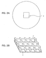
- FIG. 2A is a plane 'view of a. stencil mask produced by a method of producing a mask according to the present embodiment, while FIG. 2B is a.perspective view enlarged with an exposure region.
- the stencil mask is arranged with an exposure region 2 irradiated with X-ray, ion beam, or electron beam at a middle portion of a substrate in disk shape for example.
- a thin film having a thickness of around 100 nm to 10 ⁇ m (hereinafter called as a "membrane") is formed with a not shown aperture pattern.
- the exposure region 2 is formed with a reinforcement portion 4 having a large thickness for reinforcing strength of the thin membrane 3.
- a region divided by the reinforcement portion 4 becomes a region enabling pattern formation.
- the above stencil mask is made by an SOI wafer for example, and the thickness of the reinforcement portion 4 is a similarly to the thickness of an 8-inch silicon wafer substrate, for example, about 725 ⁇ m.
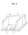
- FIG. 3 is a perspective view enlarged with a region enabling pattern formation.
- the apertures 5 corresponding to the pattern are not formed at the reinforcement portion 4, but are formed at the membrane 3 of the region enabling pattern formation.
- the pattern is constituted by the apertures 5, so the pattern such as a doughnuts pattern unable to support its middle portion cannot be formed in this shape.
- FIG. 4 is a plane view of a line-and-space pattern. If the apertures 5 of the line-and-space pattern are formed at the membrane 3, the strength of the membrane 3 drops and the washing destruction may be occurring. Due to this, the pattern like this is not applied to form in this shape. Therefore, not only the above doughnut pattern but also line-and-space pattern are carried out with a suitable division process, and have to be distributed and arranged on a mask.
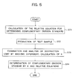
- FIG. 5 is a flow chart for determining a complementary division standard of the line-and-space pattern.
- a relative equation for determining the complementary division standard is calculated.
- the unaperture portions of the mask are considered to load.
- the load is assumed mainly surface tension of liquid.
- FIG. 6 is a view showing a step loaded to the struts by the surface tension of liquid in the step immersing a mask in liquid or drying.
- FIG. 6 is corresponding to the hatched portions of the line-and-space pattern in FIG. 4.
- the line-and-space pattern can be assumed corresponding to which the struts (beams) made by membrane having its width W L (the membrane region) are arranged at the distance W S .
- the side portions 21 of the struts shown by the hatched portions are fixed by the surrounding membrane.
- the struts constituted with the line-and-space pattern are struts structure fixed both sides, so the other side portions 22 are fixed similarly to the hatched portion side.
- the struts structure are loaded to the struts serving as the unaperture portions in wet washing of the mask and drying in maximum, when the region 23 between two struts is filled with liquid and the region outside thereof hardly ever filled with liquid. And then, the struts are acted with a pressure P in the arrow direction. This is because that if the both regions between the struts 23 are filled with liquid, the pressure is cancelled.
- ⁇ indicates the surface tension of liquid filled between the struts
- ⁇ indicates a contact angle between the struts surface contacting liquid and liquid
- W s indicates the distance between the struts shown in FIG. 6.
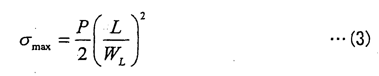
- the maximum stress ⁇ max loaded to the struts is indicated by the following equation (3) based on the following equation (2) if the width of the struts is indicated by "W L ".
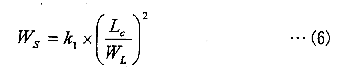
- L UL is multiplied with the suitably coefficient (safety coefficient) smaller than 1 by L c , and is indicated by the following equation (7).
- the complementary division of the stencil mask is performed by making the above L UL as the maximum volume of L, as a result the stencil mask in that washing is difficulty caused with the deformation of the struts can be provided.
- the above equations are referred to the document (Namatsu et al. Appl.Phys. Lett. Vol66 , p2656, 1995) explained with the load to the struts structure fixed one side, applied with the theory of the load to the struts structure fixed one side to the struts structure fixed both side, and calculated.
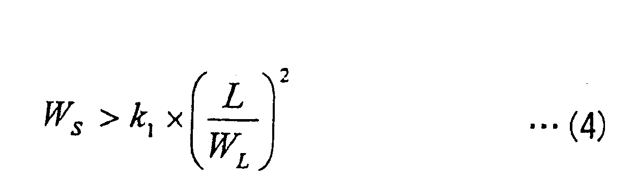
- the relative equation for the complementary division standard is calculated, then the coefficient k 1 of the above equation (5) is prepared by experiment in the struts structure fixed both side of the stencil mask. Because, the above coefficient k 1 is changed due to the Young's modulus of the membrane materials for using or a method of wet washing.
- the line-and-space pattern is formed on the membrane to produce a washing test sample so as to be able to prepare the limit length L c of the struts not deforming when washing.
- the structure of the washing test sample does not have to be equal to the membrane thickness or the membrane size of the structure of the stencil mask used for projection in practical. That is, the test sample may have the membrane materials same as the stencil mask used for projection and have a structure considered equally to the Young's modulus.
- FIG. 7A is a view showing the structure of the washing test sample.
- the respective line-and-space patterns LS nm have four struts having the length L nm , the width W Ln , and the distance W Sn shown in FIG. 7B.
- the pattern of the struts structure fixed both sides arranged with four struts shown in FIG. 7B is fixed with W L /W s by 2, and is changed with W s within the limit of 70 to 200 nm and L/W s within the limit of 5 to 200 to form the sample on a silicon membrane of about 500 nm thickness and use.
- the washing is performed at the following condition possibly close to the condition when washing the stencil mask used for projection in practical.
- the washing apparatus is used with FL820L made by Dai Nippon Screen MFG. Co., Ltd. or UW8000 made by Tokyo Electron Limited. These two apparatus are performed with the steps from washing by the plurality of washes by water or rinse chemicals to drying in single bath, that is, one bath type apparatus in that the method of replacing from pure water to chemical or replacing from chemicals to pure water is not draining at once and pouring water, but can be replacing from the previously chemicals to others gradually by the over flow.
- IPA isopropyl alcohol
- the one bath type washing apparatus can be kept with sufficiently wettability and be exchanged with chemicals. So the number of times passing through liquid-vapor interface when washing sample, that is, caused with the stress at the struts due to the surface tension, are only two when immersing a sample first in liquid and drying. Due to this, comparing with the case of using numerous bath type wet washing apparatus or a spin type washing apparatus for general use (the number of times passing though the liquid-vapor interface are increasing), the pattern deformation can be considered to small. And the spin type washing apparatus is used with a spin drying method in general. If the spin drying method is applied to the stencil mask, the centrifugal force occurs adding to the surface tension, as a result, the factors deformed with a mask pattern are increasing, and so the stress loaded to the struts is considered to increasing.
- the pulling rate and dipping rate of the sample when immersing the sample at the washing apparatus are set at the minimum rate able to self-convey in the respective apparatus.
- the flow rates for supplying liquid are set at two kinds of that one (1) is the minimum flow rate within the limit able to process automatically and the other (2) is the flow rate similarly to the real chemicals process.
- the washing process time is similaly to real chemical process. And the temperature of liquid is room tempreture, and chemicals is not used but only pure water is used.
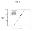
- FIG. 8 shows an experimental result in the case of washing the test sample at the above washing condition.
- the following conditions 1 to 4 are plotted with the distance W s at y-axis and (L C /W L ) 2 at x-axis.
- the difference of the conditions 1 to 4 and the coefficient k 1 calculated by parameter fitting will be mentioned hereinafter.
- the condition 1 is case of using UW8000 as the washing apparatus and employing the above (1) as the flow rate for providing liquid, so the coefficient k 1 becomes 0.22.
- the condition 2 is a case of using UW8000 as the washing apparatus and employing the above (2) as the flow rate for providing liquid, so the coefficient k 1 becomes 0.24.
- the condition 3 is a case of using FL820L as the washing apparatus and employing the above (1) as the flow rate for providing liquid, so the coefficient k 1 becomes 0.23.
- the condition 4 is a case of using FL820L as the washing apparatus and employing the above (2) as the flow rate for providing liquid, so the coefficient k 1 becomes 0.23.
- L UL shown in the above equation (7) is a function of variables W s and W L .
- the method dividing the line-and-space pattern by a division length of L UL is determined whether the entire ⁇ W s , W L , ⁇ are applied to the same A (1) or applied to same L UL (2).
- the pattern portions for complementary dividing are specified with the distances W s and the widths W L in the entire regions, then L UL are determined by the equation (7) in the respective ⁇ W s , W L ⁇ .
- WL ⁇ considered the most critical condition to the pattern deformation by washing are sampled to determine L UL in that case, and applied with the same division length to the entire ⁇ W s , W L ⁇ uniformity.
- the program according to the present embodiment is processed by computer with the complementary division process for dividing the line-and-space pattern at the complementary division condition determined like above.
- FIG. 9 is a block diagram showing an embodiment of hardware of a data processing apparatus (computer) determining the complementary division condition by reading the program according to the present embodiment.
- the data processing apparatus has an input portion 11, an output portion 12, an interface (I/F) 13, a random access memory (RAM) 14, a memory portion 15, and a central processing unit (CPU) 16. And the input portion 11, the output portion 12, the I/F 13, the RAM 14, the memory portion 15, and the CPU 16 are connected by a bus BS.
- I/F interface
- RAM random access memory
- CPU central processing unit
- the input portion 11 outputs a desired input data to the CPU 16.
- the input portion 11 is a keyboard, a mouse, a compact disc type read-only memory (CDROM) (recordable (R) or rewritable (RW)) drive, a floppy (a registered trademark) disk (FD) drive, or other input apparatus.
- CDROM compact disc type read-only memory
- R recordable
- RW rewritable
- FD floppy disk
- the output portion 12 supplies data corresponding to a desired output data outputted from the CPU 16.
- the output portion 12 is a display device and displays an image corresponding to output data outputted from the CPU 16.
- the I/F 13 transmits and receives a desired data to the other data processing apparatus according to control of the CPU 16.
- the RAM 14 is used as a workspace when the CPU 16 performs the predetermined process.
- the memory portion 15 writes and reads the desired data by the CPU 16.
- the memory portion 15 is housed with a program 150 according to the present embodiment for example.
- the program 150 includes the processing step of the complementary division process according to the present invention for example, and is performed at the RAM 14 as a workspace by the CPU 16.
- FIG. 10 is a flow chart of the complementary division process performed by the above program.
- the complementary division standard will be explained in the case of employing the above (1) method.
- a pattern is sampled from a designed pattern data, and estimated whether the sampled pattern is a pattern to be divided or not (step ST11).
- the pattern to be divided includes not only the line-and-space pattern, but also the above doughnut pattern and a leaf pattern, so if being these patterns, the respective suitable complementary division processes are performed. If not being the pattern to be divided, the division processes are not performed and portions to be distributed are determined (step ST14).
- the W L and W s of the line-and-space pattern are specified, then the division length L UL is calculated by the equation (7) and the vale of A (step ST12). That is, the W L and W s are substituted to the equation (7) to calculate the L UL , or a compensation table is prepared in advance and the W L and W s are specified to determine the L UL satisfied with the equation (7).
- the line-and-space pattern is divided at the division length determined like above (step ST13), and the divided pattern is determined with the portion to be distributed (step ST14).
- the divided pattern is distributed so as to have uniformity density. Therefore, the line-and-space pattern shown in FIG. 11A is distributed into the division pattern shown in FIG. 11B and the division pattern shown in FIG. 11C as a pair at the any portions enabling pattern formation.
- step ST15 The processes from the above step ST11 to the step ST14 are performed to the entire patterns including the pattern data (step ST15).
- an electron beam directly describing apparatus describes a complementary division pattern at a mask blanks formed with a resist on the membrane 3 using complementary divided data.
- the resist is developed, and the membrane is etched using the resist pattern as an etching mask to form apertures of the complementary division pattern at the mask blanks (step ST16).
- the resist is removed, and the stencil mask is washed by wet washing similarly to the above washing experiment to finish a process of producing the stencil mask.
- the wafer formed with the resist is exposed with shifting the stencil mask at several times, so the wafer is jointly transferred with the division pattern divided complementary to form the pattern before dividing (step ST18).
- the complementary division process shown in FIG. 10 shows an example dividing according to the complementary division standard shown in case (1), but the complementary division standard shown in case (2) may be used.
- the step ST12 is not performed and the sampled line-and-space pattern is applied with uniformity division length.
- the entire line-and-space pattern is divided in the longitudinal direction at the division length of 2 ⁇ m.
- the subsequent steps are similarly to the mention above.
- the line-and-space pattern is determined with a rule for determining the division length able to suppress the pattern deformation when wet washing in advance, determined with the suitable division length in each time according to the width and distance of the pattern of the respective line-and-space pattern, and divided in the longitudinal direction. Therefore, the line-and-space can be suitably divided by simple algorithm.
- the width and distance of the pattern that is assumed the pattern deformation over the elasticity limit is easiest given by wet washing are determined. with the definite division length able to suppress the pattern deformation when wet washing, then the entire line-and-space patterns are divided at the determined division length in the longitudinal direction. As a result, the line-and-space patterns can be suitably divided by simpler algorithm.
- the result obtained by the test sample is applied to a theory of the load to the struts structure fixed both sides, so the rule for determining the above division length or the suitable division length is calculated. As a result, the washing destruction of the stencil mask in practical can be suppressed certainly.
- the method of producing the stencil mask applied with the above complementary division method can suppress a washing destruction of the stencil mask, so can produce the stencil mask having reliability with no pattern deformation.
- the pattern deformation by wet washing of the stencil mask can be suppressed.
- the coefficient k 1 is prepared by the experiment, but may be prepared by using the values of ⁇ , ⁇ , and ⁇ c prepared from documents or by experiment each other.
Landscapes
- Physics & Mathematics (AREA)
- General Physics & Mathematics (AREA)
- Electron Beam Exposure (AREA)
- Preparing Plates And Mask In Photomechanical Process (AREA)
- Cleaning By Liquid Or Steam (AREA)
Abstract
Description

Claims (11)
- A complementary division method for dividing a pattern comprising apertures formed at a mask, comprising a step of dividing the pattern to be divided at a division length able to suppress a pattern deformation when wet washing, in the longitudinal direction of the pattern.
- A complementary division method as set forth in claim 1, comprising the steps of:determining said division length of said pattern according to a width and distance of said pattern, said division length being defined as that the maximum stress loaded to a film between said patterns is not over an elasticity limit of said film when wet washing; anddividing said pattern to be divided by said division length according to said width and distance of said pattern in said longitudinal direction.
- A complementary division method as set forth in claim 1, comprising the steps of:determining said division length of said patterns at a pattern having the smallest width and distance in said pattern to be divided, said division length being defined. as that the maximum stress loaded to a film between said patterns is not over an elasticity limit of said film'when wet washing; anddividing the entire patterns to be divided by said division length in said longitudinal direction.
- A complementary division method as set forth in claim 3, wherein said division length is no more than 2 µm.
- A method of producing a mask comprising the steps of:sampling a pattern to be divided from a designed pattern and dividing said sampled pattern to be divided by a division length able to suppress a pattern deformation in the longitudinal direction of the pattern when wet washing;distributing said divided patterns to difference regions to determine an arrangement of said divided patterns;forming apertures of said divided patterns based on the determined arrangement of said divided patterns at the different regions of a mask blanks; andwet-washing a mask formed with said aperture.
- A method of producing a mask as set forth in claim 5, comprising the steps of:determining a division length of said pattern according to a width and distance of said pattern, said division length being defined as that the maximum stress loaded to a film between said patterns is not over an elasticity limit of said film when wet washing; anddividing said pattern to be divided by said division length according to said width and distance of said pattern to be divided in said longitudinal direction.
- A method of producing a mask as set forth in claim 5, comprising the steps of:determining said division length of said patterns with a pattern having the smallest width and distance in said pattern to be divided; anddividing the entire patterns to be divided by said division length in said longitudinal direction.
- A method of producing a mask as set forth in claim 7, wherein said division length is no more than 2 µm.
- A program processed in a computer for making a complementary division process for dividing a pattern comprising apertures formed at a mask, wherein a division length of said pattern is determined according to a width and distance of said pattern, said division length being defined as that the maximum stress loaded to film between said pattern is not over an elasticity limit of said film when wet washing, said program comprising the following steps processed by the computer:sampling a pattern to be divided from a designed pattern;determining said division length according to said width and distance of said pattern; anddividing said sampled pattern to be divided by said determined division length in said longitudinal direction of the pattern.
- A program processed in a computer making a complementary division process dividing a pattern comprising apertures formed at a mask, wherein a division length of a pattern having the smallest width and distance in the pattern to be divided is determined, said division length being defined as that the maximum stress loaded to film between said patterns is not over an elasticity limit of said film when wet washing, said program comprising the following steps processed by the computer of:sampling said pattern to be divided from a designed pattern; anddividing said sampled pattern to be divided by said division length in said longitudinal direction.
- A program as set forth in claim 10, wherein said division length is no more than 2 µm.
Applications Claiming Priority (2)
| Application Number | Priority Date | Filing Date | Title |
|---|---|---|---|
| JP2003193722 | 2003-07-08 | ||
| JP2003193722A JP2005032825A (en) | 2003-07-08 | 2003-07-08 | Complementary division method, mask manufacturing method and program |
Publications (2)
| Publication Number | Publication Date |
|---|---|
| EP1496393A2 true EP1496393A2 (en) | 2005-01-12 |
| EP1496393A3 EP1496393A3 (en) | 2006-05-24 |
Family
ID=33447987
Family Applications (1)
| Application Number | Title | Priority Date | Filing Date |
|---|---|---|---|
| EP04016013A Withdrawn EP1496393A3 (en) | 2003-07-08 | 2004-07-07 | Complementary division mask, method of producing mask, and program |
Country Status (5)
| Country | Link |
|---|---|
| US (1) | US7247410B2 (en) |
| EP (1) | EP1496393A3 (en) |
| JP (1) | JP2005032825A (en) |
| KR (1) | KR20050006081A (en) |
| TW (1) | TW200507061A (en) |
Families Citing this family (3)
| Publication number | Priority date | Publication date | Assignee | Title |
|---|---|---|---|---|
| KR100800817B1 (en) * | 2006-12-27 | 2008-02-01 | 동부일렉트로닉스 주식회사 | Dividing Method of Semiconductor Circuit Pattern |
| KR20130081528A (en) * | 2012-01-09 | 2013-07-17 | 삼성디스플레이 주식회사 | Evaporation mask and evaporation apparatus using the same |
| CN115266333A (en) * | 2022-07-08 | 2022-11-01 | 重庆大学 | Method for determining maximum stress of circular film with limited maximum deflection under uniformly distributed load |
Family Cites Families (7)
| Publication number | Priority date | Publication date | Assignee | Title |
|---|---|---|---|---|
| US6180289B1 (en) * | 1997-07-23 | 2001-01-30 | Nikon Corporation | Projection-microlithography mask with separate mask substrates |
| JP3223142B2 (en) * | 1997-08-22 | 2001-10-29 | チッソ株式会社 | Manufacturing method of liquid crystal display element |
| JP3479024B2 (en) | 2000-03-28 | 2003-12-15 | Necエレクトロニクス株式会社 | Electron beam exposure mask and pattern design method thereof |
| WO2002021582A1 (en) * | 2000-09-05 | 2002-03-14 | Hoya Corporation | Transfer mask, method of dividing pattern of transfer mask, and method of manufacturing transfer mask |
| US6855467B2 (en) * | 2000-09-05 | 2005-02-15 | Hoya Corporation | Transfer mask, method of dividing pattern or transfer mask, and method of manufacturing transfer mask |
| US6830852B2 (en) * | 2001-07-19 | 2004-12-14 | Nikon Corporation | Stencil reticles for use in charged-particle-beam microlithography, and pattern-determination methods for such reticles |
| JP3903947B2 (en) * | 2003-04-16 | 2007-04-11 | ソニー株式会社 | Complementary division method |
-
2003
- 2003-07-08 JP JP2003193722A patent/JP2005032825A/en active Pending
-
2004
- 2004-07-07 EP EP04016013A patent/EP1496393A3/en not_active Withdrawn
- 2004-07-07 TW TW093120399A patent/TW200507061A/en unknown
- 2004-07-07 US US10/885,822 patent/US7247410B2/en not_active Expired - Fee Related
- 2004-07-08 KR KR1020040052926A patent/KR20050006081A/en not_active Withdrawn
Also Published As
| Publication number | Publication date |
|---|---|
| EP1496393A3 (en) | 2006-05-24 |
| US20050008948A1 (en) | 2005-01-13 |
| KR20050006081A (en) | 2005-01-15 |
| TW200507061A (en) | 2005-02-16 |
| JP2005032825A (en) | 2005-02-03 |
| US7247410B2 (en) | 2007-07-24 |
Similar Documents
| Publication | Publication Date | Title |
|---|---|---|
| KR100272797B1 (en) | Resist pattern formation method and resist pattern | |
| US6453274B2 (en) | Method of forming a pattern using proximity-effect-correction | |
| US6916582B2 (en) | Mask for fabrication of semiconductor devices, process for production of the same, and process for fabrication of semiconductor devices | |
| US20170053056A1 (en) | Method of Mask Data Synthesis and Mask Making | |
| US6447960B2 (en) | Electron beam exposure mask and pattern designing method thereof | |
| US6475684B2 (en) | Method of correcting line width variation due to loading effect caused during etching of a photomask and recording medium formed according to the method | |
| US20080153009A1 (en) | Exposure mask, optical proximity correction device, optical proximity correction method, manufacturing method of semiconductor device, and optical proximity correction program | |
| US7247410B2 (en) | Complementary division mask, method of producing mask, and program | |
| US6210842B1 (en) | Method for fabricating stencil mask | |
| JPH11126824A (en) | Pattern design method | |
| US6773854B2 (en) | Method of producing a perforated mask for particle radiation | |
| JP4314998B2 (en) | Circuit pattern dividing method, stencil mask manufacturing method, stencil mask, and exposure method | |
| US5999720A (en) | Post exposure bake simulation method | |
| US6789250B2 (en) | Pattern data generation system, method and program for pattern data generation, reticle fabricating method, and semiconductor device manufacturing method using the pattern data | |
| JP2002099073A (en) | Semiconductor circuit design pattern data correction method, photomask using corrected design pattern data, photomask inspection method, and photomask inspection pattern data production method | |
| JP2003017397A (en) | Stencil mask, method of manufacturing the same, semiconductor device manufactured using the stencil mask, and method of manufacturing the same | |
| KR100688483B1 (en) | Method of correcting line width change due to loading effect occurring during dry etching of wafer or material layer on the wafer | |
| JP2000058444A (en) | Pattern forming method and semiconductor device manufacturing method | |
| JP4425720B2 (en) | Pattern formation method | |
| JP2000323372A (en) | Proximity effect correction method and semiconductor device manufacturing method using the same | |
| US20090162789A1 (en) | Method for Transferring a Predetermined Pattern Reducing Proximity Effects | |
| JP4657646B2 (en) | Mask pattern arranging method, mask manufacturing method, semiconductor device manufacturing method, program | |
| JP2002174908A (en) | Developing method and device manufacturing method | |
| KR940002762B1 (en) | Design method of test element group of semiconductor device | |
| JPH11354423A (en) | Proximity effect correction method |
Legal Events
| Date | Code | Title | Description |
|---|---|---|---|
| PUAI | Public reference made under article 153(3) epc to a published international application that has entered the european phase |
Free format text: ORIGINAL CODE: 0009012 |
|
| AK | Designated contracting states |
Kind code of ref document: A2 Designated state(s): AT BE BG CH CY CZ DE DK EE ES FI FR GB GR HU IE IT LI LU MC NL PL PT RO SE SI SK TR |
|
| AX | Request for extension of the european patent |
Extension state: AL HR LT LV MK |
|
| PUAL | Search report despatched |
Free format text: ORIGINAL CODE: 0009013 |
|
| RIC1 | Information provided on ipc code assigned before grant |
Ipc: G03F 1/16 20060101AFI20060328BHEP |
|
| AK | Designated contracting states |
Kind code of ref document: A3 Designated state(s): AT BE BG CH CY CZ DE DK EE ES FI FR GB GR HU IE IT LI LU MC NL PL PT RO SE SI SK TR |
|
| AX | Request for extension of the european patent |
Extension state: AL HR LT LV MK |
|
| 17P | Request for examination filed |
Effective date: 20061027 |
|
| AKX | Designation fees paid |
Designated state(s): DE FR |
|
| STAA | Information on the status of an ep patent application or granted ep patent |
Free format text: STATUS: THE APPLICATION HAS BEEN WITHDRAWN |
|
| 18W | Application withdrawn |
Effective date: 20071121 |