EP1494257A1 - Plasma display panel and plasma display - Google Patents
Plasma display panel and plasma display Download PDFInfo
- Publication number
- EP1494257A1 EP1494257A1 EP03811950A EP03811950A EP1494257A1 EP 1494257 A1 EP1494257 A1 EP 1494257A1 EP 03811950 A EP03811950 A EP 03811950A EP 03811950 A EP03811950 A EP 03811950A EP 1494257 A1 EP1494257 A1 EP 1494257A1
- Authority
- EP
- European Patent Office
- Prior art keywords
- electrodes
- barrier ribs
- electrode
- disposed
- plasma display
- Prior art date
- Legal status (The legal status is an assumption and is not a legal conclusion. Google has not performed a legal analysis and makes no representation as to the accuracy of the status listed.)
- Withdrawn
Links
Images





Classifications
-
- G—PHYSICS
- G09—EDUCATION; CRYPTOGRAPHY; DISPLAY; ADVERTISING; SEALS
- G09G—ARRANGEMENTS OR CIRCUITS FOR CONTROL OF INDICATING DEVICES USING STATIC MEANS TO PRESENT VARIABLE INFORMATION
- G09G3/00—Control arrangements or circuits, of interest only in connection with visual indicators other than cathode-ray tubes
- G09G3/20—Control arrangements or circuits, of interest only in connection with visual indicators other than cathode-ray tubes for presentation of an assembly of a number of characters, e.g. a page, by composing the assembly by combination of individual elements arranged in a matrix no fixed position being assigned to or needed to be assigned to the individual characters or partial characters
- G09G3/22—Control arrangements or circuits, of interest only in connection with visual indicators other than cathode-ray tubes for presentation of an assembly of a number of characters, e.g. a page, by composing the assembly by combination of individual elements arranged in a matrix no fixed position being assigned to or needed to be assigned to the individual characters or partial characters using controlled light sources
- G09G3/28—Control arrangements or circuits, of interest only in connection with visual indicators other than cathode-ray tubes for presentation of an assembly of a number of characters, e.g. a page, by composing the assembly by combination of individual elements arranged in a matrix no fixed position being assigned to or needed to be assigned to the individual characters or partial characters using controlled light sources using luminous gas-discharge panels, e.g. plasma panels
- G09G3/288—Control arrangements or circuits, of interest only in connection with visual indicators other than cathode-ray tubes for presentation of an assembly of a number of characters, e.g. a page, by composing the assembly by combination of individual elements arranged in a matrix no fixed position being assigned to or needed to be assigned to the individual characters or partial characters using controlled light sources using luminous gas-discharge panels, e.g. plasma panels using AC panels
- G09G3/291—Control arrangements or circuits, of interest only in connection with visual indicators other than cathode-ray tubes for presentation of an assembly of a number of characters, e.g. a page, by composing the assembly by combination of individual elements arranged in a matrix no fixed position being assigned to or needed to be assigned to the individual characters or partial characters using controlled light sources using luminous gas-discharge panels, e.g. plasma panels using AC panels controlling the gas discharge to control a cell condition, e.g. by means of specific pulse shapes
- G09G3/294—Control arrangements or circuits, of interest only in connection with visual indicators other than cathode-ray tubes for presentation of an assembly of a number of characters, e.g. a page, by composing the assembly by combination of individual elements arranged in a matrix no fixed position being assigned to or needed to be assigned to the individual characters or partial characters using controlled light sources using luminous gas-discharge panels, e.g. plasma panels using AC panels controlling the gas discharge to control a cell condition, e.g. by means of specific pulse shapes for lighting or sustain discharge
-
- H—ELECTRICITY
- H01—ELECTRIC ELEMENTS
- H01J—ELECTRIC DISCHARGE TUBES OR DISCHARGE LAMPS
- H01J11/00—Gas-filled discharge tubes with alternating current induction of the discharge, e.g. alternating current plasma display panels [AC-PDP]; Gas-filled discharge tubes without any main electrode inside the vessel; Gas-filled discharge tubes with at least one main electrode outside the vessel
- H01J11/20—Constructional details
- H01J11/22—Electrodes, e.g. special shape, material or configuration
- H01J11/32—Disposition of the electrodes
-
- G—PHYSICS
- G09—EDUCATION; CRYPTOGRAPHY; DISPLAY; ADVERTISING; SEALS
- G09G—ARRANGEMENTS OR CIRCUITS FOR CONTROL OF INDICATING DEVICES USING STATIC MEANS TO PRESENT VARIABLE INFORMATION
- G09G3/00—Control arrangements or circuits, of interest only in connection with visual indicators other than cathode-ray tubes
- G09G3/20—Control arrangements or circuits, of interest only in connection with visual indicators other than cathode-ray tubes for presentation of an assembly of a number of characters, e.g. a page, by composing the assembly by combination of individual elements arranged in a matrix no fixed position being assigned to or needed to be assigned to the individual characters or partial characters
- G09G3/22—Control arrangements or circuits, of interest only in connection with visual indicators other than cathode-ray tubes for presentation of an assembly of a number of characters, e.g. a page, by composing the assembly by combination of individual elements arranged in a matrix no fixed position being assigned to or needed to be assigned to the individual characters or partial characters using controlled light sources
- G09G3/28—Control arrangements or circuits, of interest only in connection with visual indicators other than cathode-ray tubes for presentation of an assembly of a number of characters, e.g. a page, by composing the assembly by combination of individual elements arranged in a matrix no fixed position being assigned to or needed to be assigned to the individual characters or partial characters using controlled light sources using luminous gas-discharge panels, e.g. plasma panels
- G09G3/288—Control arrangements or circuits, of interest only in connection with visual indicators other than cathode-ray tubes for presentation of an assembly of a number of characters, e.g. a page, by composing the assembly by combination of individual elements arranged in a matrix no fixed position being assigned to or needed to be assigned to the individual characters or partial characters using controlled light sources using luminous gas-discharge panels, e.g. plasma panels using AC panels
- G09G3/291—Control arrangements or circuits, of interest only in connection with visual indicators other than cathode-ray tubes for presentation of an assembly of a number of characters, e.g. a page, by composing the assembly by combination of individual elements arranged in a matrix no fixed position being assigned to or needed to be assigned to the individual characters or partial characters using controlled light sources using luminous gas-discharge panels, e.g. plasma panels using AC panels controlling the gas discharge to control a cell condition, e.g. by means of specific pulse shapes
- G09G3/293—Control arrangements or circuits, of interest only in connection with visual indicators other than cathode-ray tubes for presentation of an assembly of a number of characters, e.g. a page, by composing the assembly by combination of individual elements arranged in a matrix no fixed position being assigned to or needed to be assigned to the individual characters or partial characters using controlled light sources using luminous gas-discharge panels, e.g. plasma panels using AC panels controlling the gas discharge to control a cell condition, e.g. by means of specific pulse shapes for address discharge
-
- G—PHYSICS
- G09—EDUCATION; CRYPTOGRAPHY; DISPLAY; ADVERTISING; SEALS
- G09G—ARRANGEMENTS OR CIRCUITS FOR CONTROL OF INDICATING DEVICES USING STATIC MEANS TO PRESENT VARIABLE INFORMATION
- G09G3/00—Control arrangements or circuits, of interest only in connection with visual indicators other than cathode-ray tubes
- G09G3/20—Control arrangements or circuits, of interest only in connection with visual indicators other than cathode-ray tubes for presentation of an assembly of a number of characters, e.g. a page, by composing the assembly by combination of individual elements arranged in a matrix no fixed position being assigned to or needed to be assigned to the individual characters or partial characters
- G09G3/22—Control arrangements or circuits, of interest only in connection with visual indicators other than cathode-ray tubes for presentation of an assembly of a number of characters, e.g. a page, by composing the assembly by combination of individual elements arranged in a matrix no fixed position being assigned to or needed to be assigned to the individual characters or partial characters using controlled light sources
- G09G3/28—Control arrangements or circuits, of interest only in connection with visual indicators other than cathode-ray tubes for presentation of an assembly of a number of characters, e.g. a page, by composing the assembly by combination of individual elements arranged in a matrix no fixed position being assigned to or needed to be assigned to the individual characters or partial characters using controlled light sources using luminous gas-discharge panels, e.g. plasma panels
- G09G3/288—Control arrangements or circuits, of interest only in connection with visual indicators other than cathode-ray tubes for presentation of an assembly of a number of characters, e.g. a page, by composing the assembly by combination of individual elements arranged in a matrix no fixed position being assigned to or needed to be assigned to the individual characters or partial characters using controlled light sources using luminous gas-discharge panels, e.g. plasma panels using AC panels
- G09G3/298—Control arrangements or circuits, of interest only in connection with visual indicators other than cathode-ray tubes for presentation of an assembly of a number of characters, e.g. a page, by composing the assembly by combination of individual elements arranged in a matrix no fixed position being assigned to or needed to be assigned to the individual characters or partial characters using controlled light sources using luminous gas-discharge panels, e.g. plasma panels using AC panels using surface discharge panels
- G09G3/2983—Control arrangements or circuits, of interest only in connection with visual indicators other than cathode-ray tubes for presentation of an assembly of a number of characters, e.g. a page, by composing the assembly by combination of individual elements arranged in a matrix no fixed position being assigned to or needed to be assigned to the individual characters or partial characters using controlled light sources using luminous gas-discharge panels, e.g. plasma panels using AC panels using surface discharge panels using non-standard pixel electrode arrangements
- G09G3/2986—Control arrangements or circuits, of interest only in connection with visual indicators other than cathode-ray tubes for presentation of an assembly of a number of characters, e.g. a page, by composing the assembly by combination of individual elements arranged in a matrix no fixed position being assigned to or needed to be assigned to the individual characters or partial characters using controlled light sources using luminous gas-discharge panels, e.g. plasma panels using AC panels using surface discharge panels using non-standard pixel electrode arrangements with more than 3 electrodes involved in the operation
-
- H—ELECTRICITY
- H01—ELECTRIC ELEMENTS
- H01J—ELECTRIC DISCHARGE TUBES OR DISCHARGE LAMPS
- H01J11/00—Gas-filled discharge tubes with alternating current induction of the discharge, e.g. alternating current plasma display panels [AC-PDP]; Gas-filled discharge tubes without any main electrode inside the vessel; Gas-filled discharge tubes with at least one main electrode outside the vessel
- H01J11/10—AC-PDPs with at least one main electrode being out of contact with the plasma
- H01J11/12—AC-PDPs with at least one main electrode being out of contact with the plasma with main electrodes provided on both sides of the discharge space
-
- H—ELECTRICITY
- H01—ELECTRIC ELEMENTS
- H01J—ELECTRIC DISCHARGE TUBES OR DISCHARGE LAMPS
- H01J11/00—Gas-filled discharge tubes with alternating current induction of the discharge, e.g. alternating current plasma display panels [AC-PDP]; Gas-filled discharge tubes without any main electrode inside the vessel; Gas-filled discharge tubes with at least one main electrode outside the vessel
- H01J11/20—Constructional details
- H01J11/22—Electrodes, e.g. special shape, material or configuration
- H01J11/28—Auxiliary electrodes, e.g. priming electrodes or trigger electrodes
-
- H—ELECTRICITY
- H01—ELECTRIC ELEMENTS
- H01J—ELECTRIC DISCHARGE TUBES OR DISCHARGE LAMPS
- H01J11/00—Gas-filled discharge tubes with alternating current induction of the discharge, e.g. alternating current plasma display panels [AC-PDP]; Gas-filled discharge tubes without any main electrode inside the vessel; Gas-filled discharge tubes with at least one main electrode outside the vessel
- H01J11/20—Constructional details
- H01J11/34—Vessels, containers or parts thereof, e.g. substrates
- H01J11/36—Spacers, barriers, ribs, partitions or the like
-
- G—PHYSICS
- G09—EDUCATION; CRYPTOGRAPHY; DISPLAY; ADVERTISING; SEALS
- G09G—ARRANGEMENTS OR CIRCUITS FOR CONTROL OF INDICATING DEVICES USING STATIC MEANS TO PRESENT VARIABLE INFORMATION
- G09G2320/00—Control of display operating conditions
- G09G2320/02—Improving the quality of display appearance
- G09G2320/0209—Crosstalk reduction, i.e. to reduce direct or indirect influences of signals directed to a certain pixel of the displayed image on other pixels of said image, inclusive of influences affecting pixels in different frames or fields or sub-images which constitute a same image, e.g. left and right images of a stereoscopic display
Definitions
- the present invention relates to a plasma display panel and a plasma display device used as a display device and the like, and more specifically relates to a technique for improving a state of a discharge.
- PDPs plasma display panels
- the PDPs are display devices which realize a color display by irradiating phosphors (of red, green and blue) with ultraviolet rays, which is generated when a discharge of plasma is caused in a gas, so as to obtain visible light.
- one of conventional PDPs has barrier ribs which physically isolate cells from other adjacent cells.
- FIG.11 shows an exploded perspective view of a PDP 2000 which has such barrier ribs.
- the PDP 2000 has the following configuration.
- a front plate 1090 and a back plate 1091 are disposed so as to face each other's principal surface. These plates are disposed one on top of another and sealed at peripheral edges of the plates with sealing glass (not shown in the figure) so that a discharge space 1101 is formed between them.
- the front plate 1090 includes a front glass substrate 1101, a display electrode 1102, a display electrode 1103, a dielectric layer 1106, and a protective layer 1107.
- the front glass substrate 1101 is a substrate of the front plate 1090.
- the display electrode 1102 and the display electrode 1103 are disposed on the front glass substrate 1101.
- the display electrode 1102, the display electrode 1103, and the front glass substrate are coated with the dielectric layer 1106 and the protective layer 1107.
- the protective layer 1107 is made of magnesium oxide (MgO).
- the back plate 1091 includes a back glass substrate 1111, an address electrode 1112, a dielectric layer 1113, a shadow mask 1114 which forms parallel crosses with a bottom, and phosphor layers 1115r, 1115g, and 1115b which are formed on the inside surface of the shadowmask 1114.
- the phosphor layers 1115r, 1115g, and 1115b correspond to red, green, and blue respectively.
- the shadow mask 1114 works as the barrier rib of the PDP, and forms parallel crosses with a bottom as described above.
- the shadow mask 1114 is made of Invar or the like, having a low expansion rate and flexible workability, and is composed of a parallel part 1114a, which is parallel to the address electrode 1112, an orthogonal part 1114b, which is at right angles to the address electrode 1112, and a plane part 1114c, which has a platy shape and in contact with a dielectric layer 1113.
- the discharge space 1101 is filled with a discharge gas which is composed of rare gases, such as He, Xe, and Ne.
- the vicinity of an area where a pair of the display electrode 1102 and the display electrode 1103 cross one address electrode 107 over the discharge space 1101 corresponds to a cell that contributes to image display.
- FIG.11 shows adjacent cells each of which is divided at its center.
- the phosphor layers 1115r, 1115g, and 1115b are formed on the wall surface of the depression part of the shadow mask 1114, except on a center line area 1114d which is in the vicinity of the address electrode 1112.
- the shadowmaskmade from metal intervenes between the display electrode and the address electrode. Therefore, the whole region of the shadow mask inevitably has the same electric potential.
- the general driving method for AC type PDPs in which the addressing is performed using the discharge between the display electrode and the address electrode, and a sustain discharge is performed between the pair of the display electrodes for surface discharge, becomes unavailable.
- the above-described PDP 2000 performs an opposed-discharge type light emission with use of a discharge between the display electrode 1102 or the display electrode 1103 and the address electrode 1112, which is different from the normal surface-discharge type PDPs.
- the present invention aims to provide a plasma display panel and a plasma display device in which the state of discharge is improved.
- the object can be achieved by a plasma display panel in which a plurality of pairs of first and second electrodes are disposed on a first substrate so as to be parallel to each other, a plurality of third electrodes are disposed on a second substrate, and main parts of a plurality of barrier ribs are disposed between adjacent third electrodes, the third electrodes being orthogonal to a longitudinal direction of display electrodes each of which consists of a pair of the first and second electrodes, wherein a plurality of fourth electrodes are fixed to the barrier ribs or areas of a surface of the first substrate facing the barrier ribs so as to be at least in vicinities of areas between adjacent display electrodes, the fourth electrodes being electrically exposed to discharge spaces which are defined by the barrier ribs.
- the adjacent display electrodes become electrically, not physically, isolated from each other.
- the fourth electrodes work as barriers against charge transfer, which prevent the cross talk.
- the fourth electrodes may be at a first distance from the first substrate, and fixed to the barrier ribs in such a manner as to be inserted in the barrier ribs or disposed on surfaces of the barrier ribs.
- the distance between the fourth electrodes and the first substrate can be set freely.
- the fourth electrodes are inserted in the barrier ribs, there is no fourth electrode on top of the barrier ribs.
- the first substrate faces the top surfaces of the barrier ribs which can be molded flexibly. Therefore, it becomes easy to create gaps as gas flowpaths between the first substrate and the barrier ribs.
- the fourth electrodes may be disposed on top of the barrier ribs.
- the fourth electrodes can be formed on top of the barrier ribs with use of a conventional method for forming barrier ribs.
- the plasma display panel may further comprise a plurality of fifth electrodes which are inserted in the barrier ribs at a second distance from the first substrate.
- Sub-parts of the barrier ribs which bridge adjacent main parts of the barrier ribs, may be substantially orthogonal to the third electrodes, the fourth electrodes may be fixed to the main parts of the barrier ribs, and the fifth electrodes may be fixed to the sub-parts of the barrier ribs.
- the discharge is caused along at least a part of the barrier ribs. This enables the fourth electrodes and the fifth electrodes to prevent the cross talk which occurs between cells which are adjacent in the direction of the charge transfer.
- Sub-parts of the barrier ribs, which bridge adjacent main parts of the barrier ribs, may be substantially orthogonal to the third electrodes.
- the object can be achieved by a plasma display device in which a plurality of pairs of first and second electrodes are disposed on a first substrate so as to be parallel to each other, a plurality of third electrodes are disposed on a second substrate, andmain parts of a plurality of barrier ribs are disposedbetween adjacent third electrodes, the third electrodes being orthogonal to a longitudinal direction of display electrodes each of which consists of a pair of the first and second electrodes, wherein a plurality of fourth electrodes are fixed to the barrier ribs so as to be at least in vicinities of areas between adjacent display electrodes, the fourth electrodes being electrically exposed to discharge spaces which are defined by the barrier ribs, and the plasma display device includes a driving circuit for applying a voltage to the fourth electrode or for earthing the fourth electrodes.
- the adjacent display electrodes By applying voltages to the fourth electrodes which are disposed in vicinity of areas between adjacent display electrodes, the adjacent display electrodes become electrically, not physically, isolated from each other. As a result, the cross talk can be prevented.
- the state of the discharge caused in the PDP can be improved.
- the driving circuit may apply positive voltages to the fourth electrodes.
- the adjacent display electrodes By applying positive voltages to the fourth electrodes which are disposed in vicinities of areas between adjacent display electrodes, the adjacent display electrodes become electrically, not physically, isolated from each other. As a result, the cross talk can be prevented.
- the fourth electrodes may be at a first distance from the first substrate, and fixed to the barrier ribs in such a manner as to be inserted in the barrier ribs or disposed on surfaces of the barrier ribs.
- the distance between the fourth electrodes and the first substrate can be set freely.
- the fourth electrodes may be disposed on top of the barrier ribs.
- the fourth electrodes can be formed on top of the barrier ribs with use of a conventional method for forming barrier ribs.
- the driving circuit may apply a first voltage pulse and a second voltage pulse to the first electrodes and the second electrodes respectively, and additionally apply a third voltage pulse to the fourth electrodes.
- voltages can be applied to fourth electrodes and the fifth electrodes individually, and more accurate discharge control can be performed.
- the plasma display device may further comprise a plurality of fifth electrodes which are inserted in the barrier ribs at a second distance from the first substrate, wherein the driving circuit applies a fourth voltage pulse to the fifth electrodes when outputting the first voltage pulse and the second voltage pulse at the same time.
- an AC discharge is caused by applying voltages to the first electrodes and the second electrodes alternately.
- the negative charges are inductively accelerated by the fourth electrodes which exist in the vicinity. This realizes a driving with low electric power.
- Sub-parts of the barrier ribs which bridge adjacent main parts of the barrier ribs, may be substantially orthogonal to the third electrodes, the fourth electrodes may be fixed to the main parts of the barrier ribs, and the fifth electrodes may be fixed to the sub-parts of the barrier ribs.
- the discharge is caused along at least a part of the barrier ribs.
- voltage control according to the direction of the charge transfer can be realized.
- Sub-parts of the barrier ribs, which bridge adjacent main parts of the barrier ribs, may be substantially orthogonal to the third electrodes.
- FIG.1 is a block diagram which shows the overall configuration of the AC type PDP device according to the present invention.
- the PDP device 1000 includes a panel unit 100 for displaying images, and a display driving unit 200 for driving the panel unit 100 based on the intra-field time division gradation display technique.
- FIG.2 is a perspective view which typically shows the configuration of the panel unit 100.
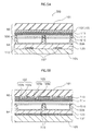
- FIG. 3A is a cross-sectional view of the panel unit 100 taken along the line B-B'
- FIG. 3B is a cross-sectional view of the panel unit 100 taken along the line A-A'.
- the panel unit 100 comprises the front plate 90 and the back plate 91 which are disposed so as to face each other's principal surface, and these plates are disposed one on top of another and sealed at peripheral edges of the plates with sealing glass (not shown in the figure) so that a discharge space 92 is formed between them.
- the front plate 90 includes a front glass substrate 101, a scan electrode 102 as an example of the first electrode, a sustain electrode 103 as an example of the second electrode, a dielectric layer 113, and a protective layer 114.
- the front glass substrate 101 is a substrate of the front plate 90.
- the scan electrode 102 and the sustain electrode 103 are disposed on the front glass substrate 101.
- the scan electrode 102 and the sustain electrode 103 are formed in the following manner:
- Conductive metal oxide such as ITO (Indium Tin Oxide), SnO 2 , and ZnO is layered on the front glass substrate 101 with use of the sputteringmethod, the vacuum vapor deposition method, the CVD method, spraying method, or the like, and transparent electrodes 102a and 103a (shown in FIG.3B) are formed by patterning the layers so as to have a certain width and certain intervals with use of lithography. Then, bus electrodes 102b and 103b are formed by layering silver (Ag) on the transparent electrodes 102a and 103a with use of techniques within public domain, such as the thick-film forming method.
- ITO Indium Tin Oxide
- SnO 2 Tin Oxide
- ZnO ZnO
- the dielectric layer 113 is formed on the front glass substrate 101, on which the scan electrode and the sustain electrode 103 are formed, in the manner that the front glass substrate is covered with the dielectric layer 113.
- the protective layer 102 which is made of magnesium oxide (MgO), is formed.
- the back plate 91 includes a back glass substrate 105, an address electrode 107 as an example of a third electrode, a dielectric layer 123, a barrier rib 106, a guide electrode 108 as an example of a fourth electrode, and a phosphor layer 115 formed on the barrier rib 106.
- the phosphor layer 115 corresponds to one of red green and blue.
- the barrier rib 106 is made of insulative material, a plurality of which form parallel crosses crossing at right angles.
- the barrier rib 106 is composed of a parallel part 106a, which is parallel to the address electrode 107 as FIG.3A shows, and an orthogonal part 106b, which is at right angles to the address electrode 107 as FIG.3B shows.
- This barrier rib 106 is formed by the screen printing with use of a photomask, or by the sandblasting.
- the guide electrode 108 is made of conductive material, a plurality of which form parallel crosses crossing at right angles.
- the guide electrode 108 is disposed on the top of the barrier rib 106.
- the guide electrode 108 is disposed on the top of the barrier rib with use of techniques within public domain, such as the vacuum vapor deposition method and the thick-film forming method. The description of how to dispose the guide electrode is omitted here.
- the display driving unit 200 evenly applies voltage of electropositive potential over the guide electrode 108.
- the discharge space 92 is filled with a discharge gas which is composed of rare gases, such as He, Xe, and Ne.
- the vicinity of an area where a pair of the scan electrode 102 and the sustain electrode 103 cross one address electrode 107 over the discharge space 92 corresponds to a cell that contributes to image display.
- the above-described phosphor layer 115 is formed on the wall surface of the above-described barrier ribs.
- the dielectric layers 113 and 123 which are included in the front plate 90 and the back plate 91 respectively, are formed by applying an organic binder including lead glass with a low melting point and bismuth glass with a low melting point, and baking the applied organic binder.
- the protective layer 102 is a thin film made of Magnesium oxide (MgO).
- the display driving unit 200 includes a data detection unit 210, a subfield conversion unit 220, a display control unit 240, a sustain driver 250, a scan driver 260, a data driver 270, and a constant voltage applying unit 280.
- the data detection unit 210 detects image data (gradation values for each cell) of each picture from video data, which is inputted externally and indicates gradation values of each discharge cell included in the panel unit 100. Then, the data detection unit 210 sequentially transmits the detected data to the subfield conversion unit 220.
- the detection of image data of each picture can be performed based on a vertical synchronous signal included in the video data.
- the subfield conversion unit 220 includes a subfieldmemory 221.
- the subfield conversion unit 220 converts the image data transmitted from the data detection unit 210 into subfield data which is a group of binary data indicating ON or OFF of cells for gradational display. Then, the subfield data is to be stored in the subfield memory 221.
- the subfield data is outputted to the data driver 270 under control of display control unit 240.
- Synchronous signals such as a horizontal synchronous signal (Hsync) and a vertical synchronous signal (Vsync) are inputted to the display control unit 240 in synchronization with the above-described video data.
- Hsync horizontal synchronous signal
- Vsync vertical synchronous signal
- the display control unit 240 outputs, based on the inputted synchronous signals, a timing signal to the data detection unit 210 for indicating timing for transmitting the image data, a timing signal to the subfield conversion unit 220 for indicating timing for writing/reading to/from the subfield memory 221, and timing signals to the sustain driver 250, scan driver 260, and data driver 270 for indicating timing for applying each pulse voltage.
- the sustain driver 250 uses an integrated driver circuit within public domain, and is connected to a plurality of sustain electrodes 103 which is disposed on the front plate 90 included in the panel unit 100.
- the sustain driver 250 applies, to a plurality of sustain electrodes 103, an initialization pulse, an address pulse (approximately +180V), and a sustain pulse which varies from 0V to a predetermined voltage (+180V to +220V, preferably +200V) during an initialization period and a sustain period of each subfield for performing steady initialization discharge, sustain discharge, and erase discharge in all the discharge cells.
- the scan driver 260 uses an integrated driver circuit within public domain, and is connected to a plurality of scan electrodes 102 which is disposed on the front plate 90 included in the panel unit 100.
- the scan driver 260 applies, to each of a plurality of scan electrodes 102, an initialization pulse, an address pulse (approximately +100V), and a sustain pulse which varies from 0V to a predetermined voltage (+180V to +220V, preferably +200V) during the initialization period, the address period, and the sustain period of each subfield for performing steady initialization discharge, address discharge, and sustain discharge in all the discharge cells.
- the data driver 270 uses an integrated driver circuit within public domain (e.g. the integrated driver circuit described in FIG. 1 of the Japanese unexamined patent publication NO.2002-287691), and is connected to each of a plurality of address electrodes 107 which is disposed on the back plate 91 included in the panel unit 100.
- the data driver 270 selectively applies, to a plurality of address electrodes 107, an address pulse which is 0V or a predetermined voltage (+60V to +90V, preferably +75V) during the address period of each subfield for performing steady address discharge and sustain discharge in all the discharge cells.
- the constant voltage applying unit 280 applies, to the guide electrode 108, a predetermined constant voltage (-150V to +220V, preferably +30V to +150V) during the driving.
- the addressing is performed so as to form wall charges only in the cells which are to emit light with the discharge between the scan electrode 102 and the address electrode 107. Also, the light emission with the surface discharge is sustained by the discharge between the scan electrode 102 and its corresponding sustain electrode 103.
- the charge transfer caused by the discharge between the scan electrode 102 and the sustain electrode 103 is kept in the area surrounded with the guide electrode 108. This is by the effect of repulsive force, which is formed in the vicinity of the guide electrode 108 by applying positive voltage to the guide electrode 108 which surrounds the scan electrode102 and its corresponding sustain electrode 103. As a result, the charge transfers between adjacent cells are effectively prevented.
- the cross talk is prevented because the adjacent cells are electrically, not physically, isolated from each other by the guide electrodes 108 disposed on the border of the adjacent cells.
- the discharge becomes stable by this driving method. As a result, an anomalous discharge and a failure of addressing are prevented as well.
- the influence of the electric field over the address discharge between the scan electrode 102 and the address electrode 107 is reduced, because the guide electrode 108 is disposed on the top of the barrier rib 106, which is distant from the address electrode 107.
- the state of the address discharge is kept well, and prevention of the cross talk and stabilization of the address discharge are realized at the same time.
- the discharge is kept well as well.
- the effective area of the cell is broadened and a high-luminance, high-resolution display is realized with the above configuration.
- a predetermined constant voltage (-150V to +220V, preferably +30V to +150V) is applied to the guide electrode 108, which is the fourth electrode, however, the cross talk is also prevented by earthing the fourth electrode, just as the earthing for keeping the isolationbetween electrodes of a semiconductor or the like, because the display electrodes in the adjacent cells are electrically isolated from each other.
- the guide electrode 108 of the panel unit 100 in the first embodiment is disposed on the top of the barrier rib 106, however, the guide electrode 108 may be disposed on the wall surface of the front plate 90 which faces to the top of the barrier rib 106.
- the guide electrode 108 is disposed on the protective layer 114 so as to surround each cell by forming parallel crosses.
- the guide electrode 108 as an example of the fourth electrode may be disposed, along the borders of cells, on the side of the front plate 90.
- the addressing with the conventional driving method for the AC type PDP with address discharge is available, because there is no metal part between the display electrode and the address electrode, unlike the conventional PDP 2000.
- the difference between the above-described panel unit 100 according to the first embodiment and the panel unit 500 is only in the configuration of the back plate.
- the panel unit 500 is driven by the display driving unit 200 just as the PDP device 1000.
- the guide electrode is disposed at a different position from that of the panel unit 100.
- FIG.4 is a perspective view which typically shows the configuration of the panel unit 500.
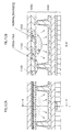
- FIG.5A is a cross-sectional view of the panel unit 500 taken along the line D-D'
- FIG.5B is a cross-sectional view of the panel unit 500 taken along the line C-C'.
- the back plate 94 is different from the back plate 91 in that the guide electrode 510 as an example of the fourth electrode is inserted in the barrier rib 506, not disposed on the top of the barrier rib.
- the insertion position is at a certain distance in the direction of height from the inside surface of the front plate 90, near the top of the barrier rib 506.
- a certain distance in the direction of height from the inside surface of the front plate 90 means a distance which is not more than a half of the height of the barrier rib.
- the guide electrode 510 is a electrode made of conductive material, a plurality of which form parallel crosses, just as the guide electrode 108 of the first embodiment.
- the distance between the guide electrode 510 and the inside surface of the front plate 90 is longer than that in the panel unit 100.
- FIG. 5A shows, a part of the barrier rib 606 which is parallel to the address electrode 107 substantially touches the inside surface of the front plate 90.
- substantially touches means that there may be no gap, or a very narrow gap.
- FIG.5B shows, between a part of the barrier rib 606 which is orthogonal to the address electrode 107 and the inside surface of the front plate 90, there is a wide gap.
- This gap works as a flow path for releasing an impure gas.
- the barrier rib 606 and the guide electrode 510 with the above-described configuration are formed in the following manner: Firstly, a barrier rib which is lower than the barrier rib 106 in the first embodiment is formed with use of the technique within public domain which is described in the first embodiment; Secondly, the guide electrode is formed by layering conductive materials on the top surface of the barrier rib; Finally, an insulative barrier rib is added onto the top of the guide electrode 510 with use of the above-described technique within public domain.
- the panel unit 500 according to the second embodiment has the wide gap or the gas flow path between the part of the barrier rib 606 which is orthogonal to the address electrode 107 and the inside surface of the front plate 90. This gap brings benefit that the release of impure gases and filling of gasses are performed quickly.
- the state of the address discharge is kept well, and both prevention of the cross talk and stabilization of the address discharge are realized, just as in the first embodiment.
- the guide electrode 510 is inserted in the barrier rib 503.
- the insertion position is at a certain distance from the inside surface of the front plate 90, near the top of the barrier rib 506. This means that the guide electrode 510 is distant from the address electrode 107.
- the influence of the electric field over the address discharge between the scan electrode 102 and the address electrode 107 is reduced, the state of the address discharge is kept well, and prevention of the cross talk and stabilization of the address discharge are realized at the same time.
- the addressing with the conventional driving method for the AC type PDP with address discharge is available, because there is no metal part between the display electrode and the address electrode unlike the conventional PDP 2000.
- the PDP device 1500 includes a panel unit 100 for displaying images, and a display driving unit 201 for driving the panel unit 100 based on the intra-field time division gradation display technique.
- the display driving unit 201 is different from the display driving unit 200 of the first and second embodiment only in the manner of applying voltage to the guide electrode.
- the following is a detailed description of the display driving unit 201.
- a display control unit 239 instead of the display control unit 240, is disposed in the display driving unit 201 as FIG.6 shows.
- a pulse generator 275 is added between a guide electrode control unit 241 and the guide electrode 108.
- the pulse generator 275 applies, to the guide electrode 108, a pulse voltage which varies from 0V to a predetermined voltage (-150V to +220V, preferably +30V to +150V) while receiving timing signals from the guide electrode control unit 241.
- the pulse generator 275 receives a signal which instructs the pulse generator 275 to apply a positive constant voltage to the guide electrode 108, the pulse generator 275 applies a positive constant voltage to the guide electrode 108.
- the display control unit 239 includes the guide electrode control unit 241.
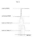
- the guide electrode control unit 241 outputs the timing signal to the pulse generator 275 so that a pulse applied to the guide electrode rises at t -1 , which is 100nsec before t 0 , and falls at t 1 , which is 100nsec after t 0 .
- the sign to represents a time when a pulse applied to the sustain electrode 103 rises up.
- the timing of this rising up is the same timing as a voltage V 1 applied to the scan electrode 102 (100V ⁇ V 1 ⁇ 300V) with a pulse width t W1 (10nsec ⁇ t W1 ⁇ 1 ⁇ sec) falls down.
- the phase of the pulse applied to the sustain electrode 103 is completely opposite to that of the voltage V 1 .
- the guide electrode control unit 241 outputs, during the address period, a signal which instructs the pulse generator to apply a positive constant voltage to the guide electrode 108.
- an AC discharge is caused by applying voltages to the guide electrode 108 and the scan electrode 102 alternately.
- a voltage is applied to the guide electrode 108 so that the period in which the voltage pulse applied to the scan electrode 102 falls down and the period in which the voltage pulse applied to the sustain electrode 103 rises up overlap each other.
- the negative charges are inductively accelerated by the guide electrode 108 which exist in the vicinity. This realizes a discharge with a low voltage and a driving with low electric power.
- the state of the discharge is improved just as the panel unit 100 in the first embodiment and the panel unit 500 in the second embodiment.
- the discharge is kept well as well.
- the effective area of the cell is broadened and a high-luminance, high-resolution display can be realized.
- the guide electrode 108 is distant from the address electrode 107 just as in the first embodiment and the second embodiment. As a result, the influence of the electric field over the address discharge between the scan electrode 102 and the address electrode 107 is reduced, the state of the address discharge is kept well, and prevention of the cross talk and stabilization of the address discharge are realized at the same time.
- the panel unit 100 is driven by the display driving unit 201, however, the panel unit 500 may be used instead of the panel unit 100, because both of themhave the same basic characteristics and in both cases, prevention of a cross talk, an anomalous discharge, a failure of addressing, and so on is realized, and the light emission becomes more efficient.
- the value of the time parameter which is set to the guide electrode control unit 241 and the value of the voltage parameter which is set to the pulse generator 275 are based on the common positional relation between cells of PDPs which are commercially available at present. Therefore, those values and the shape of the pulses waves may differ according to the cell size and the positional relation between the cells.
- the guide electrode control unit 241 applies a signal which instructs the pulse generator 275 to apply a positive constant voltage to the guide electrode 108, however, the guide electrode control unit 241 may apply a signal which instructs the pulse generator 275 to earth the guide electrode 108 during the address period.
- the PDP device 1600 includes a panel unit 600 for displaying images, and a display driving unit 202 for driving the panel unit 600 based on the intra-field time division gradation display technique.
- the PDP device 1600 in the fourth embodiment is different from the PDP device 1000 in the first embodiment in the configuration of the panel unit and the display driving unit.
- the panel unit 600 in the fourth embodiment is different from the panel unit 100 in the first embodiment in the configuration of the back plate.
- the panel unit 600 two guide electrodes, which are different in direction, are disposed on the back plate 95. In this point, the panel unit 600 is different from the panel unit 100 and the panel unit 500.
- a guide electrode 610 as an example of the fourth electrode is inserted in the barrier rib 606 so as to form right angles with the address electrode 107.
- the insertion position is at a certain distance in the direction of height from the inside surface of the front plate 90 (The position is near the front plate 90, and the case where the distance to the front plate 90 is zero is excluded).
- the guide electrode 611 as an example of the fifth electrode, which is parallel to the address electrode 107 is disposed on the top of the barrier rib 606.
- a certain distance in the direction of height from the inside surface of the front plate 90 means a distance which is not more than a half of the height of the barrier rib. There is a gap between the guide electrode 611 and the inside surface of the front plate 90, which works as a gas flow path.
- guide electrodes 610 and 611 are disposed on the barrier rib 606 with use of the technique within public domain. Therefore, the description of how to dispose the guide electrodes is omitted here.
- a guide electrode control unit 241 is added to the display control unit 240 included in the display driving unit 201.
- a pulse generator 276 is added between a guide electrode control unit 241 and the guide electrode 108.
- the pulse generator 275 applies, to the guide electrode 610, a pulse voltage which varies from 0V to a predetermined voltage (-150V to +220V, preferably +30V to +150V) while receiving timing signals from the guide electrode control unit 241, and the pulse generator 276 applies, to the guide electrode 611, a pulse voltage which varies from 0V to a predetermined voltage (-150V to +220V, preferably +30V to +150V) while receiving timing signals from the guide electrode control unit 242.
- the maximum value of the voltage which is applied to the guide electrode 611 is set to be less than the maximum value of the voltage which is applied to the guide electrode 610.
- the operation of the guide electrode control unit 241 is the same as that described in the third embodiment.
- the guide electrode control unit 242 outputs the timing signal to the pulse generator 276 so that the rising timing of the pulse which is applied to the guide electrode 611 becomes t 2 , which is 10nsec to 1 ⁇ sec after the rising timing of the pulse which is applied to the guide electrode 610, and the falling timing of the pulse which is applied to the guide electrode 611 becomes t 3 , which is 10nsec to 1 ⁇ sec after the falling timing of the pulse which is applied to the guide electrode 610.
- the area in which the plasma discharge occurs is extended in the cells toward the back panel.
- the pulse waveform and the timing of applying the pulse for removing the cross talks between cells and the anomalous discharges can be determined and applied to the guide electrode 610 which is disposed so as to form right angles with the address electrode 107, and the area in which plasma discharge occurs can be extended in the cells toward the back panel by the effect of guide electrode 611 which is disposed to be parallel to the address electrode107.
- the guide electrode 610 and the guide electrode 611 are distant from the address electrode 107 just as in the first, second, and third embodiment. As a result, the influence of the electric field over the address discharge between the scan electrode 102 and the address electrode 107 is reduced, the state of the address discharge is kept well, and prevention of the cross talk and stabilization of the address discharge are realized at the same time.
- the value of the time parameter which is set to the guide electrode control units 241 and 242, and the value of the voltage parameter which is set to the pulse generators 275 and 276 are based on the common positional relation between cells of PDPs which are commercially available at present. Therefore, those values and the shape of the pulse waves may differ according to the cell size and the positional relation between the cells.
- the guide electrode 611 as an example of the fifth electrode is disposed on the top of the barrier rib 606, however, the guide electrode 611 may be disposed on the wall surface of the front plate which faces to the top of the barrier rib 606.
- the guide electrode 611 is formed on the top surface of two walls out of four, which surround each cell on the side of the front plate 90.
- the two walls are parallel to the display electrode.
- the addressing with the conventional driving method for the AC type PDP with address discharge is available, because there is no metal part between the display electrode and the address electrode, unlike the conventional PDP 2000.
- the present invention is applicable to high-resolution display devices used for televisions, computer displays, and the like.
Landscapes
- Engineering & Computer Science (AREA)
- Physics & Mathematics (AREA)
- Plasma & Fusion (AREA)
- Power Engineering (AREA)
- Computer Hardware Design (AREA)
- General Physics & Mathematics (AREA)
- Theoretical Computer Science (AREA)
- Chemical & Material Sciences (AREA)
- Materials Engineering (AREA)
- Gas-Filled Discharge Tubes (AREA)
- Control Of Indicators Other Than Cathode Ray Tubes (AREA)
- Control Of Gas Discharge Display Tubes (AREA)
Abstract
Description
As FIG.8 shows, a guide
Claims (14)
- A plasma display panel in which a plurality of pairs of first and second electrodes are disposed on a first substrate so as to be parallel to each other, a plurality of third electrodes are disposed on a second substrate, and main parts of a plurality of barrier ribs are disposed between adjacent third electrodes, the third electrodes being orthogonal to a longitudinal direction of display electrodes each of which consists of a pair of the first and second electrodes, wherein
a plurality of fourth electrodes are fixed to the barrier ribs or areas of a surface of the first substrate facing the barrier ribs so as to be at least in vicinities of areas between adjacent display electrodes, the fourth electrodes being electrically exposed to discharge spaces which are defined by the barrier ribs. - The plasma display panel of Claim 1, wherein
the fourth electrodes are at a first distance from the first substrate, and fixed to the barrier ribs in such a manner as to be inserted in the barrier ribs or disposed on surfaces of the barrier ribs. - The plasma display panel of Claim 2, wherein
the fourth electrodes are disposed on top of the barrier ribs. - The plasma display panel of Claim 2, further comprising:a plurality of fifth electrodes which are inserted in the barrier ribs at a second distance from the first substrate.
- The plasma display panel of Claim 4, wherein
sub-parts of the barrier ribs, which bridge adjacent main parts of the barrier ribs, are substantially orthogonal to the third electrodes,
the fourth electrodes are fixed to the main parts of the barrier ribs, and
the fifth electrodes are fixed to the sub-parts of the barrier ribs. - The plasma display panel of any of Claim 1 to 4, wherein
sub-parts of the barrier ribs, which bridge adjacent main parts of the barrier ribs, are substantially orthogonal to the third electrodes. - A plasma display device in which a plurality of pairs of first and second electrodes are disposed on a first substrate so as to be parallel to each other, a plurality of third electrodes are disposed on a second substrate, and main parts of a plurality of barrier ribs are disposed between adjacent third electrodes, the third electrodes being orthogonal to a longitudinal direction of display electrodes each of which consists of a pair of the first and second electrodes, wherein
a plurality of fourth electrodes are fixed to the barrier ribs so as to be at least in vicinities of areas between adjacent display electrodes, the fourth electrodes being electrically exposed to discharge spaces which are defined by the barrier ribs, and
the plasma display device includes a driving circuit for applying a voltage to the fourth electrodes or for earthing the fourth electrodes. - The plasma display device of Claim 7, wherein
the driving circuit applies a positive voltage to the fourth electrodes. - The plasma display device of Claim 8, wherein
the fourth electrodes are at a first distance from the first substrate, and fixed to the barrier ribs in such a manner as to be inserted in the barrier ribs or disposed on surfaces of the barrier ribs. - The plasma display device of Claim 9, wherein
the fourth electrodes are disposed on top of the barrier ribs. - The plasma display device of Claim 10, wherein
the driving circuit applies a first voltage pulse and a second voltage pulse to the first electrodes and the second electrodes respectively, and additionally applies a third voltage pulse to the fourth electrodes. - The plasma display device of Claim 11, further comprising:a plurality of fifth electrodes which are inserted in the barrier ribs at a second distance from the first substrate, whereinthe driving circuit applies a fourth voltage pulse to the fifth electrodes when outputting the first voltage pulse and the second voltage pulse at the same time.
- The plasma display device of Claim 12, wherein
sub-parts of the barrier ribs, which bridge adjacent main parts of the barrier ribs, are substantially orthogonal to the third electrodes,
the fourth electrodes are fixed to the main parts of the barrier ribs, and
the fifth electrodes are fixed to the sub-parts of the barrier ribs. - The plasma display device of any of Claim 7 to 11, wherein
sub-parts of the barrier ribs, which bridge adjacent main parts of the barrier ribs, are substantially orthogonal to the third electrodes.
Applications Claiming Priority (5)
| Application Number | Priority Date | Filing Date | Title |
|---|---|---|---|
| JP2002345497 | 2002-11-28 | ||
| JP2002345497 | 2002-11-28 | ||
| JP2003133077 | 2003-05-12 | ||
| JP2003133077 | 2003-05-12 | ||
| PCT/JP2003/015213 WO2004049377A1 (en) | 2002-11-28 | 2003-11-28 | Plasma display panel and plasma display |
Publications (2)
| Publication Number | Publication Date |
|---|---|
| EP1494257A1 true EP1494257A1 (en) | 2005-01-05 |
| EP1494257A4 EP1494257A4 (en) | 2008-06-25 |
Family
ID=32396289
Family Applications (1)
| Application Number | Title | Priority Date | Filing Date |
|---|---|---|---|
| EP03811950A Withdrawn EP1494257A4 (en) | 2002-11-28 | 2003-11-28 | PLASMA PANEL AND PLASMA SCREEN |
Country Status (6)
| Country | Link |
|---|---|
| US (1) | US20050218805A1 (en) |
| EP (1) | EP1494257A4 (en) |
| JP (1) | JPWO2004049377A1 (en) |
| KR (1) | KR20050084786A (en) |
| TW (1) | TW200414260A (en) |
| WO (1) | WO2004049377A1 (en) |
Families Citing this family (7)
| Publication number | Priority date | Publication date | Assignee | Title |
|---|---|---|---|---|
| TWI240942B (en) * | 2004-05-25 | 2005-10-01 | Chunghwa Picture Tubes Ltd | Method of depositing phosphor onto the shadow mask of plasma flat panel display by utilizing electrophoretic deposition method |
| KR100615253B1 (en) * | 2004-09-24 | 2006-08-25 | 삼성에스디아이 주식회사 | Driving Method of Plasma Display Panel |
| KR20060073328A (en) * | 2004-12-24 | 2006-06-28 | 엘지전자 주식회사 | Plasma Display Panel And Method Of Manufacturing The Same |
| KR100745536B1 (en) * | 2005-08-01 | 2007-08-03 | 쓰리엠 이노베이티브 프로퍼티즈 캄파니 | Separation device and control method for PD panel assembly |
| EP2219202B1 (en) * | 2009-02-17 | 2013-11-20 | Samsung SDI Co., Ltd. | Plasma display panel and method of manufacturing the same |
| KR20110039838A (en) * | 2009-10-12 | 2011-04-20 | 삼성에스디아이 주식회사 | Plasma display panel |
| KR101082445B1 (en) * | 2009-10-30 | 2011-11-11 | 삼성에스디아이 주식회사 | Plasma display panel |
Family Cites Families (9)
| Publication number | Priority date | Publication date | Assignee | Title |
|---|---|---|---|---|
| JPS5810350A (en) * | 1981-06-23 | 1983-01-20 | Fujitsu Ltd | Self-shift-type gas electric-discharge panel |
| JP2963515B2 (en) * | 1990-09-20 | 1999-10-18 | 富士通株式会社 | Plasma display panel and driving method thereof |
| JPH10149771A (en) * | 1996-11-18 | 1998-06-02 | Hitachi Ltd | Plasma display panel and method of manufacturing the same |
| JPH11120919A (en) * | 1997-10-09 | 1999-04-30 | Hitachi Ltd | Plasma display panel |
| JP2000188063A (en) * | 1998-12-21 | 2000-07-04 | Mitsubishi Electric Corp | Substrate for AC plasma display panel, AC plasma display panel, and method of driving AC plasma display panel |
| KR100304906B1 (en) * | 1999-02-24 | 2001-09-26 | 구자홍 | Plasma Display Panel having Floating electrode |
| JP3737010B2 (en) * | 2000-02-04 | 2006-01-18 | パイオニア株式会社 | Plasma display panel |
| JP2001266750A (en) * | 2000-03-22 | 2001-09-28 | Fujitsu Hitachi Plasma Display Ltd | Plasma display panel |
| JP4177969B2 (en) * | 2001-04-09 | 2008-11-05 | 株式会社日立製作所 | Plasma display panel |
-
2003
- 2003-11-28 TW TW092133546A patent/TW200414260A/en unknown
- 2003-11-28 US US10/511,062 patent/US20050218805A1/en not_active Abandoned
- 2003-11-28 EP EP03811950A patent/EP1494257A4/en not_active Withdrawn
- 2003-11-28 JP JP2005510292A patent/JPWO2004049377A1/en active Pending
- 2003-11-28 KR KR1020047017377A patent/KR20050084786A/en not_active Withdrawn
- 2003-11-28 WO PCT/JP2003/015213 patent/WO2004049377A1/en not_active Ceased
Also Published As
| Publication number | Publication date |
|---|---|
| KR20050084786A (en) | 2005-08-29 |
| JPWO2004049377A1 (en) | 2006-03-30 |
| TW200414260A (en) | 2004-08-01 |
| US20050218805A1 (en) | 2005-10-06 |
| WO2004049377A1 (en) | 2004-06-10 |
| EP1494257A4 (en) | 2008-06-25 |
Similar Documents
| Publication | Publication Date | Title |
|---|---|---|
| JP2000331615A (en) | Plasma display panel and driving method thereof | |
| EP1174851A2 (en) | Plasma display panel and method and apparatus for driving the same | |
| US7106278B2 (en) | Plasma display panel and driving method thereof | |
| EP1494257A1 (en) | Plasma display panel and plasma display | |
| US20050093776A1 (en) | Plasma display device and method for driving same | |
| US20030038757A1 (en) | Plasma display apparatus and driving method thereof | |
| CN101635243A (en) | plasma display panel | |
| US20040239589A1 (en) | Plasma display panel apparatus and drive method thereof | |
| US20060214884A1 (en) | Plasma display panel driving method and plasma display apparatus | |
| KR100501981B1 (en) | Plasma display panel | |
| KR100324261B1 (en) | Plasma Display Panel and Method of Driving the same | |
| JPH10302643A (en) | Plasma display panel and driving method thereof | |
| US7687994B2 (en) | Plasma display panel (PDP) | |
| EP1752951A1 (en) | Method of driving plasma display panel and plasma display apparatus driven using the method | |
| CN100385598C (en) | Plasma display panel and plasma display device | |
| KR100683795B1 (en) | Driving Method of Plasma Display Panel | |
| KR100659084B1 (en) | Multi-electrode Plasma Display Panel | |
| JP2001068030A (en) | 3-electrode AC plasma display panel | |
| KR20060067420A (en) | Multi-electrode Plasma Display Panel and Plasma Display Device | |
| JP2002343259A (en) | Plasma display device | |
| KR100592312B1 (en) | Multi-electrode Plasma Display Panel | |
| JP3764897B2 (en) | Driving method of plasma display panel | |
| KR100499080B1 (en) | Plasma display panel | |
| JP2003331731A (en) | Plasma display device | |
| KR20090014862A (en) | Driving device for display panel and driving method thereof |
Legal Events
| Date | Code | Title | Description |
|---|---|---|---|
| PUAI | Public reference made under article 153(3) epc to a published international application that has entered the european phase |
Free format text: ORIGINAL CODE: 0009012 |
|
| 17P | Request for examination filed |
Effective date: 20041013 |
|
| AK | Designated contracting states |
Kind code of ref document: A1 Designated state(s): AT BE BG CH CY CZ DE DK EE ES FI FR GB GR HU IE IT LI LU MC NL PT RO SE SI SK TR |
|
| A4 | Supplementary search report drawn up and despatched |
Effective date: 20080527 |
|
| RIC1 | Information provided on ipc code assigned before grant |
Ipc: G09G 3/28 20060101ALI20080520BHEP Ipc: H01J 17/49 20060101AFI20080520BHEP |
|
| STAA | Information on the status of an ep patent application or granted ep patent |
Free format text: STATUS: THE APPLICATION HAS BEEN WITHDRAWN |
|
| 18W | Application withdrawn |
Effective date: 20080805 |