EP1492247A1 - Störfeste Eingangsstufe einer Zweidrahtleitung - Google Patents
Störfeste Eingangsstufe einer Zweidrahtleitung Download PDFInfo
- Publication number
- EP1492247A1 EP1492247A1 EP03360076A EP03360076A EP1492247A1 EP 1492247 A1 EP1492247 A1 EP 1492247A1 EP 03360076 A EP03360076 A EP 03360076A EP 03360076 A EP03360076 A EP 03360076A EP 1492247 A1 EP1492247 A1 EP 1492247A1
- Authority
- EP
- European Patent Office
- Prior art keywords
- circuit
- wire line
- potential
- voltage
- contact
- Prior art date
- Legal status (The legal status is an assumption and is not a legal conclusion. Google has not performed a legal analysis and makes no representation as to the accuracy of the status listed.)
- Granted
Links
- 230000011664 signaling Effects 0.000 claims abstract description 13
- 238000000034 method Methods 0.000 claims abstract description 6
- 230000008054 signal transmission Effects 0.000 claims abstract description 3
- 238000006073 displacement reaction Methods 0.000 claims description 6
- 230000000694 effects Effects 0.000 claims description 5
- 230000001143 conditioned effect Effects 0.000 claims description 2
- 230000008878 coupling Effects 0.000 description 4
- 238000010168 coupling process Methods 0.000 description 4
- 238000005859 coupling reaction Methods 0.000 description 4
- 238000004088 simulation Methods 0.000 description 4
- 238000012544 monitoring process Methods 0.000 description 2
- 230000005540 biological transmission Effects 0.000 description 1
- 239000003990 capacitor Substances 0.000 description 1
- 239000004020 conductor Substances 0.000 description 1
- 230000001934 delay Effects 0.000 description 1
- 238000000926 separation method Methods 0.000 description 1
Images

Classifications
-
- H—ELECTRICITY
- H04—ELECTRIC COMMUNICATION TECHNIQUE
- H04B—TRANSMISSION
- H04B3/00—Line transmission systems
- H04B3/02—Details
- H04B3/32—Reducing cross-talk, e.g. by compensating
-
- H—ELECTRICITY
- H04—ELECTRIC COMMUNICATION TECHNIQUE
- H04L—TRANSMISSION OF DIGITAL INFORMATION, e.g. TELEGRAPHIC COMMUNICATION
- H04L25/00—Baseband systems
- H04L25/02—Details ; arrangements for supplying electrical power along data transmission lines
- H04L25/08—Modifications for reducing interference; Modifications for reducing effects due to line faults ; Receiver end arrangements for detecting or overcoming line faults
- H04L25/085—Arrangements for reducing interference in line transmission systems, e.g. by differential transmission
Definitions
- the invention relates to a circuit, in particular an input stage of a two-wire line having at least a first and a second contact for connecting a two-wire line, wherein the first contact is connected to a power supply and the circuit has an output contact for a conditioned digitized output signal.
- a data transmission over two-wire lines is used, for example, in railway signaling.
- there are also other areas of application such as the signaling in the monitoring of a factory site or in the object monitoring.
- Current loop signaling used typically loop currents in the range 4 - 20 mA are used.
- the coupling capacity of two-wire line pairs for example, in a quadrupole cable, so large that a mutual influence of the line pairs can occur. If an alternating voltage is transmitted in a two-wire line, this alternating voltage can be coupled into the other two-wire lines due to the coupling capacity, which depending on the cable design can be 40 - 150 nF / km.
- the coupled-in AC voltage can lead to undesired signal changes of a circuit connected to a two-wire line into which the AC voltage is coupled, in particular if the two-wire line is used for current loop signaling.
- the object of the invention is to provide a circuit with which the disturbing influence of a coupled Mesh is safely avoided.
- the potential shift by the potential shifter causes no current to be drawn from a current source disposed in the circuit, and thus a switching element that causes a change in the output signal does not switch.
- the potential displacement device can be realized with standard components, so that there is a great deal of freedom in the choice of the components.
- the potential shift device can be adapted depending on the expected coupled AC voltage or circuit design.
- the potential shifter acts primarily when the connected two-wire line is open on the transmitter side, i. not shorted.
- the simplest arrangement of the potential shifter is between the contacts within the circuit. However, it could also be arranged outside the circuit between the lines of the two-wire line.
- the potential shifter for example, the potential is shifted by about 100V.
- the second contact may be connected to ground.
- the first contact is connected directly or indirectly to the supply voltage.
- the potential displacement device is designed as a diode or transistor.
- the potential increasing device can be realized in a particularly simple manner.
- the diode does not affect the circuit, in particular to the output signal. However, it reliably prevents a faulty output signal due to a coupled-in AC voltage when the two-wire line is open. When using a transistor, this would have to be connected or driven in order to effect a potential shift of the coupled-in AC voltage.
- the circuit has a switching element which is in contact with the output contact. This allows in Connection with the connected two-wire line a current loop signaling.
- the circuit represents the receiver side. If the two-wire line is not short-circuited on the transmitter side, the switching element is in a first state. If the two-wire line is short-circuited on the transmitter side, a current flows from a current source via the switching element, through the short-circuited two-wire line and back again to the circuit. In this case, the state of the switching element is changed, so that the signal level changes at its output. This means that the loop current is only provided by the receiver.
- the switching element is preferably designed as an optocoupler, opto-field effect transistor, opto-thyristor or opto-triac. If an optocoupler is used, the voltage source may be floating (floating) or grounded at any point. This means, in particular, that the second contact can be connected to ground, but does not have to be connected to ground. In principle, the positive or negative pole, or the associated contact, can be grounded.
- the circuit can be protected by safely keeping the injected AC voltage away from the switching element and the remaining circuitry. This can be done in a particularly simple manner by a second diode which is arranged between the first contact and the switching element. This diode is used in particular for the protection of the electronics of the two-wire line input stage.
- the circuit can be active, in particular, the switching state of the switching element can change.
- a filter be provided between the switching element and the output contact. If the circuit is designed such that a change in the switching state of the switching element is to be expected in particular in the case of negative voltage peaks of the coupled-in AC voltage, the filter is advantageously designed as a low-pass filter.
- the output signal is provided by an inverter, which may be designed as a Schmitt trigger. This ensures that there is a digitized output signal.
- the inverter can be connected downstream of the filter.
- the object is also achieved by a method for interference-proof transmission of signals via a two-wire line, in which the potential of the mean value of a coupled into the two-wire line, the output signal of a circuit connected to the two-wire line disturbing alternating voltage is shifted to another potential, in particular higher potential in such a way that the output signal of the circuit remains unchanged when the interference voltage is coupled in.
- the potential can be shifted in the positive or negative direction. It depends on the circuit design and / or the supply voltage of the circuit how far the potential has to be shifted in order to avoid the influence of disturbing coupled AC voltages. Coupled AC voltages are particularly a problem when the two-wire line is open on the transmitter side, i. not shorted.
- the inventive method therefore causes an avoidance of the influence of the coupled AC voltage with open two-wire line. In the case of a short-circuited two-wire line, the coupled-in AC voltage generally does not affect the output signal of the circuit anyway.
- the potential-shifted AC voltage is decoupled from the circuit. This measure protects the electronics of the circuit.
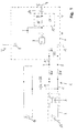
- a two-wire line 1 is connected at one end to a switching element 3 arranged as a switching relay in a transmitter 2 and at the other end to a first and second contact 4, 5 of a circuit 6 designed as an input stage of a two-wire line which outputs a digitized output signal via an output contact 7 .
- a power source 8 is connected to a power supply V cc , which supplies 24 V in the embodiment.
- the power source supplies a constant current of 5 mA.
- Downstream of the current source 8 is a switching element 9 designed as an optocoupler, which is connected to the first contact 4. Between the first contact 4 and the second contact 5 designed as a diode D2 potential displacement device is arranged.
- a second diode D1 is interposed between the first contact 4 and the switching element 9, a second diode D1 is interposed.
- current loop signaling it is provided that when the two-wire line 1 is closed, ie when the switching element 3 is closed by the transmitter 2, a current from the current source 8 via the switching element 9, the first contact 4, the first line 10 with loop resistance RW , the switching element 3 , the second line 11 with loop resistance RW , the second contact 5 to ground 12 flows.
- the output of the switching element 9 goes to the signal level "low”.
- This signal is passed through an adapted as a low-pass filter filter 13 with the components RF , CF to an inverter 14 , so that the output contact 7 of the circuit 6 is a processed and digitized output signal with the signal level "high".
- the switching element 3 is open at the transmitter, the two-wire line 1 is not short-circuited, no current flows through the switching element 9 in the circuit 6.
- the signal level is "high” and correspondingly at the output contact 7 the signal level "low” .
- the transmitter 2 is shown greatly simplified.
- a Square wave generator 15 is shown, which alternately triggers an opening and closing of the switching element 3.
- the transmitter 2 is formed, for example, as part of a railway signaling as a printed circuit board (output board) with multiple relay contacts or with multiple open-collector outputs.
- an AC voltage generator 16 is shown in FIG. 1 whose AC voltage is coupled into the two-wire line 1 via the coupling capacitors CK .
- a plurality of two-wire lines run parallel to each other, which are twisted in pairs, in particular between a transmitter and a receiver.
- An alternating voltage transmitted in one of the two-wire lines can be coupled into the two-wire line 1 on the basis of a coupling capacitance CK.
- the current source 8 can be activated, causing a change in the signal level at the output of the switching element 9 and consequently a change of the output signal at the output contact 7.
- the output signal therefore no longer reflects the switching state of the switching element 3 in the transmitter 2 and is disturbed.
- the diode D2 has the effect that, when the two-wire line 1 is open, the potential of the mean value of the coupled-in AC voltage at the point A is shifted to a higher, more positive potential, which is, in particular, higher than the positive supply voltage Vcc. Therefore, the current source 8 is not activated by the coupled AC voltage and the signal at the output of the switching element 9 as little as the output signal at the output contact 7 changed.
- the diode D1 protects the components of the circuit 6 from the coupled AC voltage, which is not necessarily sinusoidal in practice.
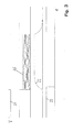
- FIG. 2 shows a simulation result of the current signaling arrangement of FIG. 1 without the diodes D1, D2.
- the voltage V is plotted along the ordinate and the time t along the abscissa.
- the signal 20 indicates the switching state, wherein the signal level "high" indicates that the switching element 3 is closed, ie the two-wire line 1 is short-circuited.
- the signal 21 shows the voltage curve at the point A in FIG. 1. As long as the two-wire line 1 is short-circuited, this point is pulled to ground, so that no appreciable voltage is present. When the two-wire line is open, the coupled-in AC voltage can be detected.
- the signal 22 represents the voltage curve at the point B in FIG. 1 again, ie at the input of the inverter 14.
- the signal 23 represents the output signal of the circuit 6 at the point C. In undisturbed two-wire line, it would have the signal 20, apart from small time delays. In Fig. 2, however, it can be seen that due to the coupled AC voltage, the signal 21 temporarily drops to such a low signal level that the signal 23 changes at the point 24, although the signal 20 remains unchanged.
- FIG. 3 shows the simulation result of the current loop signaling arrangement of FIG. 1 taking into account the diodes D1, D2.
- the coupled-in AC voltage 26 is shifted to a higher potential at the point A, ie at the contact 4, ie the mean value of the coupled-in AC voltage 26 has been shifted.
- This causes the voltage at the point B (signal 22) to remain at a high level as long as the two-wire line is open. Therefore, the output signal 23 error-free the state of the switching element 3 again.
- a circuit (6) connected to a short-circuitable two-wire line (1) has a potential displacement device with which the potential of the Mean value of a two-wire line (1) coupled noise voltage is shifted to another, in particular higher potential, so that the Störcicnaps causes no change in the output signal of the circuit (6).
Landscapes
- Engineering & Computer Science (AREA)
- Computer Networks & Wireless Communication (AREA)
- Signal Processing (AREA)
- Power Engineering (AREA)
- Arrangements For Transmission Of Measured Signals (AREA)
- Cable Transmission Systems, Equalization Of Radio And Reduction Of Echo (AREA)
- Dc Digital Transmission (AREA)
- Logic Circuits (AREA)
- Communication Cables (AREA)
- Testing Of Short-Circuits, Discontinuities, Leakage, Or Incorrect Line Connections (AREA)
- Insulated Conductors (AREA)
Abstract
Description
- Die Erfindung betrifft eine Schaltung, insbesondere eine Eingangsstufe einer Zweidrahtleitung, die mindestens einen ersten und einen zweiten Kontakt zum Anschluss einer Zweidrahtleitung aufweist, wobei der erste Kontakt mit einer Spannungsversorgung verbunden ist und die Schaltung einen Ausgangskontakt für ein aufbereitetes digitalisiertes Ausgangssignal aufweist.
- Eine Datenübertragung über Zweidrahtleitungen wird beispielsweise in der Eisenbahnsignalisierung verwendet. Es gibt jedoch auch andere Anwendungsbereiche, wie die Signalisierung bei der Überwachung eines Werkgeländes oder bei der Objektüberwachung. Häufig wird eine Stromschleifensignalisierung verwendet, wobei typischerweise Schleifenströme im Bereich 4 - 20 mA eingesetzt werden.
- Bei langen Leitungen, insbesondere von einer Länge über 10 km, wie sie im Eisenbahnbereich vorkommen können, wird die Koppelkapazität von Zweidrahtleitungspaaren, beispielsweise in einem Vierpolkabel, derart groß, dass eine gegenseitige Beeinflussung der Leitungspaare eintreten kann. Wird in einer Zweidrahtleitung eine Wechselspannung übertragen, kann diese Wechselspannung aufgrund der Koppelkapazität, die je nach Kabelausführung 40 - 150 nF/km sein kann, in die anderen Zweidrahtleitungen eingekoppelt werden. Die eingekoppelte Wechselspannung kann zu unerwünschten Signalwechseln einer an eine Zweidrahtleitung, in die die Wechselspannung eingekoppelt wird, angeschlossenen Schaltung führen, insbesondere, wenn die Zweidrahtleitung für eine Stromschleifensignalisierung verwendet wird.
- Aufgabe der Erfindung ist es, eine Schaltung bereit zu stellen, mit der der störende Einfluss einer eingekoppelten Wechselspannug sicher vermieden wird.
- Gelöst wird diese Aufgabe erfindungsgemäß durch eine Schaltung der eingangs genannten Art, bei der zwischen den Kontakten eine Potentialverschiebungseinrichtung zur Potentialverschiebung, insbesondere zur Potentialerhöhung, des Mittelwerts einer in die Zweidrahtleitung eingekoppelten Wechselspannung vorgesehen ist.
- Die Potentialverschiebung durch die Potentialverschiebungseinrichtung bewirkt, dass kein Strom von einer in der Schaltung angeordneten Stromquelle gezogen wird und folglich ein schaltendes Element, das eine Änderung des Ausgangssignals bewirkt, nicht schaltet. Die Potentialverschiebungseinrichtung kann mit Standardbauteilen realisiert werden, so dass eine große Freiheit bei der Wahl der Bauteile besteht. Die Potentialverschiebungseinrichtung kann je nach zu erwartender eingekoppelter Wechselspannung oder Schaltungsauslegung adaptiert werden. Die Potentialverschiebungseinrichtung wirkt in erster Linie, wenn die angeschlossene Zweidrahtleitung senderseitig offen ist, d.h. nicht kurzgeschlossen ist. Die einfachste Anordnung der Potentialverschiebungseinrichtung ist zwischen den Kontakten innerhalb der Schaltung. Sie könnte jedoch auch außerhalb der Schaltung zwischen den Leitungen der Zweidrahtleitung angeordnet sein. Durch die Potentialverschiebungseinrichtung wird das Potential beispielsweise um etwa 100 V verschoben. Der zweite Kontakt kann mit Masse verbunden sein. Der erste Kontakt ist mittelbar oder unmittelbar mit der Versorgungsspannung verbunden.
- Bei einer bevorzugten Ausführungsform ist die Potentialverschiebungseinrichtung als Diode oder Transistor ausgebildet. Durch diese Maßnahme kann die Potentialerhöhungseinrichtung auf besonders einfache Art und Weise realisiert werden. Bei senderseitig kurzgeschlossener Zweidrahtleitung wirkt sich die Diode nicht auf die Schaltung, insbesondere auf das Ausgangssignal aus. Sie verhindert jedoch bei offener Zweidrahtleitung zuverlässig ein fehlerhaftes Ausgangssignal aufgrund einer eingekoppelten Wechselspannung. Bei Verwendung eines Transistors müsste dieser entsprechend beschaltet bzw. angesteuert werden, um eine Potentialverschiebung der eingekoppelten Wechselspannung zu bewirken.
- Besonders bevorzugt ist es, wenn die Schaltung ein mit dem Ausgangskontakt in Verbindung stehendes Schaltelement aufweist. Dies ermöglicht in Verbindung mit der angeschlossenen Zweidrahtleitung eine Stromschleifensignalisierung. Dabei stellt die Schaltung die Empfängerseite dar. Ist die Zweidrahtleitung senderseitig nicht kurzgeschlossen, ist das Schaltelement in einem ersten Zustand. Wird die Zweidrahtleitung senderseitig kurz geschlossen, fließt ein Strom von einer Stromquelle über das Schaltelement, durch die kurzgeschlossene Zweidrahtleitung und wieder zurück zur Schaltung. Dabei wird der Zustand des Schaltelements geändert, so dass sich der Signalpegel an seinem Ausgang ändert. Dies bedeutet, dass der Schleifenstrom nur von dem Empfänger bereit gestellt wird.
- Um eine Potentialtrennung der Eingänge und des Ausgangs des Schaltelements sicher zu stellen, ist das Schaltelement vorzugsweise als Optokoppler, Opto-Feldeffekttransistor, Opto-Thyristor oder Opto-Triac ausgebildet. Wenn ein Optoelement verwendet wird, kann die Spannungsquelle erdfrei (massefrei, floating) sein oder an einem beliebigen Punkt auf Masse gelegt werden. Dies bedeutet insbesondere, dass der zweite Kontakt mit Masse verbunden sein kann, jedoch nicht mit Masse verbunden sein muss. Es kann grundsätzlich der positive oder negative Pol, bzw. der damit verbundene Kontakt, geerdet werden.
- Die Schaltung kann geschützt werden, indem die eingekoppelte Wechselspannung sicher von dem Schaltelement und der restlichen Schaltung fern gehalten wird. Dies kann auf besonders einfache Art und Weise durch eine zweite Diode geschehen, die zwischen dem ersten Kontakt und dem Schaltelement angeordnet ist. Diese Diode dient insbesondere dem Schutz der Elektronik der Zweidrahtleitungseingangsstufe.
- Bei Spitzen der eingekoppelten Wechselspannung kann die Schaltung aktiv werden, insbesondere kann sich der Schaltzustand des Schaltelements ändern. Um zu verhindern, dass dadurch das Ausgangssignal der Schaltung beeinflusst wird, kann zwischen dem Schaltelement und dem Ausgangskontakt ein Filter vorgesehen sein. Ist die Schaltung so ausgelegt, dass ein Ändern des Schaltzustands des Schaltelements insbesondere bei negativen Spannungsspitzen der eingekoppelten Wechselspannung zu erwarten ist, ist das Filter vorteilhafterweise als Tiefpassfilter ausgebildet.
- Vorzugsweise wird das Ausgangssignal durch einen Inverter, der als Schmitt-Trigger ausgebildet sein kann, bereit gestellt. Dies stellt sicher, dass ein digitalisiertes Ausgangssignal vorliegt. Der Inverter kann dem Filter nachgeschaltet sein.
- Die Aufgabe wird außerdem gelöst durch ein Verfahren zum störfesten Übertragen von Signalen über eine Zweidrahtleitung, bei dem das Potential des Mittelwerts einer in die Zweidrahtleitung eingekoppelten, das Ausgangssignal einer mit der Zweidrahtleitung verbundenen Schaltung störenden Wechselspannung auf ein anderes Potential, insbesondere höheres Potential verschoben wird, derart dass das Ausgangssignal der Schaltung bei eingekoppelter Störwechselspannung unverändert bleibt. Je nach Auslegung der Schaltung kann das Potential in positive oder negative Richtung verschoben werden. Von der Schaltungsauslegung und/oder der Versorgungsspannung der Schaltung hängt es ab, wie weit das Potential verschoben werden muss, um den Einfluss von störenden eingekoppelten Wechselspannungen zu vermeiden. Eingekoppelte Wechselspannungen sind insbesondere dann ein Problem, wenn die Zweidrahtleitung senderseitig offen, d.h. nicht kurz geschlossen ist. Das erfindungsgemäße Verfahren bewirkt daher eine Vermeidung des Einflusses der eingekoppelten Wechselspannung bei offener Zweidrahtleitung. Bei kurzgeschlossener Zweidrahtleitung wirkt sich die eingekoppelte Wechselspannung in der Regel ohnehin nicht auf das Ausgangssignal der Schaltung aus.
- Es kann vorgesehen sein, das Potential der Wechselspannung zu verschieben und dabei die Wirkung der Gleichrichtung einer Wechselspannung zu erzielen.
- Dies kann insbesondere durch eine Diode, die zwischen den Leitern der Zweidrahtleitung oder zwischen den mit den Leitungen verbundene Kontakten der Schaltung angeordnet ist, realisiert werden.
- Bei einer bevorzugten Verfahrensvariante ist vorgesehen, dass die potentialverschobene Wechselspannung von der Schaltung entkoppelt wird. Durch diese Maßnahme wird die Elektronik der Schaltung geschützt.
- Weitere Merkmale und Vorteile der Erfindung ergeben sich aus der nachfolgenden Beschreibung eines Ausführungsbeispiels der Erfindung, anhand der Figuren der Zeichnung, die erfindungswesentliche Einzelheiten zeigen, und aus den Ansprüchen. Die einzelnen Merkmale können je einzeln für sich oder zu mehreren in beliebiger Kombination bei einer Variante der Erfindung verwirklicht sein.
- Ein Ausführungsbeispiel der erfindungsgemäßen Schaltung ist in der schematischen Zeichnung dargestellt und wird in der nachfolgenden Beschreibung erläutert. Es zeigt:
- Fig. 1
- eine Anordnung für eine Stromschleifensignalisierung;
- Fig. 2
- ein Simulationsergebnis ohne Potentialverschiebung der eingekoppelten Wechselspannung;
- Fig. 3
- ein Simulationsergebnis mit Potentialverschiebung der eingekoppelten Wechselspannung.
- Eine Anordnung für eine Stromschleifensignalisierung ist in der Fig. 1 dargestellt. Eine Zweidrahtleitung 1 ist einenends mit einem in einem Sender 2 angeordneten als Schaltrelais ausgebildeten Schaltelement 3 verbunden und anderenends mit einem ersten und zweiten Kontakt 4, 5 einer als Eingangsstufe einer Zweidrahtleitung ausgebildeten Schaltung 6, die über einen Ausgangskontakt 7 ein digitalisiertes Ausgangssignal ausgibt. In der Schaltung 6 ist eine Stromquelle 8 an eine Spannungsversorgung Vcc angeschlossen, die im Ausführungsbeispiels 24 V liefert. Die Stromquelle liefert einen konstanten Strom von 5 mA. Der Stromquelle 8 nachgeschaltet ist ein als Optokoppler ausgebildetes Schaltelement 9, das mit dem ersten Kontakt 4 verbunden ist. Zwischen dem ersten Kontakt 4 und dem zweiten Kontakt 5 ist eine als Diode D2 ausgebildete Potentialverschiebungseinrichtung angeordnet. Zwischen dem ersten Kontakt 4 und dem Schaltelement 9 ist eine zweite Diode D1 zwischengeschaltet. Bei der Stromschleifensignalisierung ist vorgesehen, dass bei geschlossener Zweidrahtleitung 1, d.h. wenn vom Sender 2 das Schaltelement 3 geschlossen wird, ein Strom von der Stromquelle 8 über das Schaltelement 9, den ersten Kontakt 4, die erste Leitung 10 mit Schleifenwiderstand RW, das Schaltelement 3, die zweite Leitung 11 mit Schleifenwiderstand RW, den zweiten Kontakt 5 gegen Masse 12 fließt. Wenn ein solcher Strom fließt, geht der Ausgang des Schaltelements 9 auf den Signalpegel "low". Dieses Signal wird über ein als Tiefpassfilter ausgebildetes Filter 13 mit den Komponenten RF, CF an einen Inverter 14 weiter gegeben, so dass am Ausgangskontakt 7 der Schaltung 6 ein aufbereitetes und digitalisiertes Ausgangssignal mit dem Signalpegel "high" anliegt.
- Ist dagegen das Schaltelement 3 senderseitig geöffnet, die Zweidrahtleitung 1 also nicht kurz geschlossen, fließt kein Strom durch das Schaltelement 9 in der Schaltung 6. Am Ausgang des Schaltelements 9 liegt der Signalpegel "high" und entsprechend am Ausgangskontakt 7 der Signalpegel "low" an. An dieser Stelle ist anzumerken, dass der Sender 2 stark vereinfacht dargestellt ist. Um die Schaltungsanordnung simulieren zu können, ist ein Rechteckwellengenerator 15 dargestellt, der alternierend ein Öffnen und Schließen des Schaltelements 3 auslöst. In der Praxis ist der Sender 2 beispielsweise als Teil einer Eisenbahnsignalisierung als Leiterplatte (Ausgangsboard) mit mehreren Relaiskontakten oder mit mehreren Open-Kollektor-Ausgängen ausgebildet.
- Um den Einfluss einer parallel zur Zweidrahtleitung 1 geführten Zweidrahtleitung auf das Ausgangssignal der Schaltung 6 zu simulieren, ist in der Fig. 1 ein Wechselspannungsgenerator 16 dargestellt, dessen Wechselspannung über die Koppelkapazitäten CK in die Zweidrahtleitung 1 eingekoppelt wird. In der Praxis verlaufen mehrere Zweidrahtleitungen parallel zueinander, die paarweise miteinander verdrillt sind, insbesondere zwischen einem Sender und einem Empfänger. Eine in einer der Zweidrahtleitungen übertragene Wechselspannung kann in die Zweidrahtleitung 1 aufgrund einer Koppelkapazität CK eingekoppelt werden. Liegt der Mittelwert der eingekoppelten Wechselspannung bei offener Zweidrahtleitung 1 an der Stelle A unterhalb der Versorgungsspannung Vcc, kann die Stromquelle 8 aktiviert werden, was eine Änderung des Signalpegels am Ausgang des Schaltelements 9 bewirkt und folglich auch eine Änderung des Ausgangssignals am Ausgangskontakt 7. Das Ausgangssignal gibt daher nicht mehr den Schaltzustand des Schaltelements 3 im Sender 2 wieder und ist gestört.
- Die Diode D2 bewirkt jedoch, dass bei offener Zweidrahtleitung 1 das Potential des Mittelwerts der eingekoppelten Wechselspannung an der Stelle A auf ein höheres, positiveres Potential verschoben wird, das insbesondere höher liegt als die positive Versorgungsspannung Vcc. Daher wird durch die eingekoppelte Wechselspannung die Stromquelle 8 nicht aktiviert und das Signal am Ausgang des Schaltelements 9 ebenso wenig wie das Ausgangssignal am Ausgangskontakt 7 verändert. Die Diode D1 schützt die Bauelemente der Schaltung 6 vor der eingekoppelten Wechselspannung, die in der Praxis nicht notwendigerweise sinusförmig ist.
- In der Fig. 2 ist ein Simulationsergebnis der Stromsignalisierungsanordnung der Fig. 1 ohne die Dioden D1, D2 dargestellt. Dabei ist entlang der Ordinate die Spannung V und entlang der Abszisse die Zeit t aufgetragen. Das Signal 20 gibt den Schaltzustand wieder, wobei der Signalpegel "high" angibt, dass das Schaltelement 3 geschlossen, d.h. die Zweidrahtleitung 1 kurzgeschlossen ist. Das Signal 21 zeigt den Spannungsverlauf an der Stelle A in der Fig. 1. Solange die Zweidrahtleitung 1 kurzgeschlossen ist, wird dieser Punkt auf Masse gezogen, so dass keine nennenswerte Spannung vorhanden ist. Bei offener Zweidrahtleitung ist die eingekoppelte Wechselspannung detektierbar. Das Signal 22 gibt den Spannungsverlauf an der Stelle B in der Fig. 1 wieder, d.h. am Eingang des Inverters 14. Das Signal 23 stellt das Ausgangssignal der Schaltung 6 an der Stelle C dar. Bei ungestörter Zweidrahtleitung müsste es das Signal 20, abgesehen von geringen Zeitverzögerungen, widerspiegeln. In Der Fig. 2 ist jedoch erkennbar, dass aufgrund der eingekoppelten Wechselspannung das Signal 21 vorübergehend auf einen so geringen Signalpegel sinkt, dass sich das Signal 23 an der Stelle 24 ändert, obwohl das Signal 20 unverändert bleibt.
- In der Fig. 3 ist das Simulationsergebnis der Stromschleifensignalisierungsanordnung der Fig. 1 unter Berücksichtigung der Dioden D1, D2 dargestellt. Im Gegensatz zur Fig. 2 ist die eingekoppelte Wechselspannung 26 an der Stelle A, d.h. am Kontakt 4, zu einem höheren Potential verschoben, d.h. der Mittelwert der eingekoppelten Wechselspannung 26 wurde verschoben. Dies bewirkt, dass die Spannung an der Stelle B (Signal 22) auf einem hohen Niveau bleibt, solange die Zweidrahtleitung offen ist. Daher gibt das Ausgangssignal 23 fehlerfrei den Zustand des Schaltelements 3 wieder.
- Eine an eine kurzschließbare Zweidrahtleitung (1) angeschlossene Schaltung (6) weist eine Potentialverschiebeeinrichtung auf, mit der das Potential des Mittelwerts einer in die Zweidrahtleitung (1) eingekoppelten Störwechselspannung auf ein anderes, insbesondere höheres Potential verschoben wird, so dass die Störwechselspannung keine Änderung des Ausgangssignals der Schaltung (6) bewirkt.
Claims (10)
- Schaltung (6), insbesondere Eingangsstufe einer Zweidrahtleitung (1), die mindestens einen ersten und einen zweiten Kontakt (4, 5) zum Anschluss einer Zweidrahtleitung (1) aufweist, wobei der erste Kontakt (4) mit einer Spannungsversorgung (Vcc) verbunden ist und die Schaltung (6) einen Ausgangskontakt (7) für ein aufbereitetes digitalisiertes Ausgangssignal (23) aufweist,
dadurch gekennzeichnet,
dass zwischen den Kontakten (4, 5) eine Potentialverschiebungseinrichtung zur Potentialverschiebung, insbesondere Potentialerhöhung, des Mittelwerts einer in die Zweidrahtleitung (1) eingekoppelten Wechselspannung (26) vorgesehen ist. - Schaltung nach Anspruch 1, dadurch gekennzeichnet, dass die Potentialverschiebungseinrichtung als Diode (D2) ausgebildet ist.
- Schaltung nach Anspruch 1, dadurch gekennzeichnet, dass die Schaltung (6) ein mit dem Ausgangskontakt (7) in Verbindung stehendes Schaltelement (9) aufweist.
- Schaltung nach Anspruch 3, dadurch gekennzeichnet, dass das Schaltelement (9) als Optokoppler, Opto-Feldeffekttransistor, Opto-Thyristor oder Opto-Triac ausgebildet ist.
- Schaltung nach Anspruch 3, dadurch gekennzeichnet, dass eine zweite Diode (D1) zwischen dem ersten Kontakt (4) und dem Schaltelement (9) angeordnet ist.
- Schaltung nach Anspruch 3, dadurch gekennzeichnet, dass zwischen dem Schaltelement (9) und dem Ausgangskontakt (7) ein Filter (13), insbesondere ein Tiefpassfilter vorgesehen ist.
- Schaltung nach Anspruch 1, dadurch gekennzeichnet, dass dem Ausgangskontakt (7) ein Inverter (14) zur Digitalisierung des Ausgangssignals (23) vorgeschaltet ist.
- Stromschleifensignalisierungsanordnung umfassend einen Sender (2) mit mindestens einem Schaltelement (3), das mit einer Zweidrahtleitung (1) verbunden ist, die zu einer Schaltung (6), insbesondere nach Anspruch 1, führt und mit einer Potentialverschiebungseinrichtung, die das Potential des Mittelwerts einer in die Zweidrahtleitung (1) eingekoppelten Wechselspannung (26) derart verschiebt, dass ein Ausgangssignal (23) der Schaltung (6) durch die Wechselspannung (26) nicht gestört wird.
- Verfahren zum störfesten Übertragen von Signalen über eine Zweidrahtleitung (1), bei dem das Potential des Mittelwerts einer in die Zweidrahtleitung (1) eingekoppelten, das Ausgangssignal (23) einer mit der Zweidrahtleitung (1) verbundenen Schaltung (6) störenden Wechselspannung auf ein anderes Potential, insbesondere höheres Potential verschoben wird, derart dass das Ausgangssignal (23) der Schaltung (6) bei eingekoppelter Störwechselspannung unverändert bleibt.
- Verfahren nach Anspruch 9, dadurch gekennzeichnet, dass die potentialverschobene Wechselspannung (26) von der Schaltung (6) entkoppelt wird.
Priority Applications (3)
| Application Number | Priority Date | Filing Date | Title |
|---|---|---|---|
| AT03360076T ATE409371T1 (de) | 2003-06-25 | 2003-06-25 | Störfeste eingangsstufe einer zweidrahtleitung |
| EP03360076A EP1492247B1 (de) | 2003-06-25 | 2003-06-25 | Störfeste Eingangsstufe einer Zweidrahtleitung |
| DE50310542T DE50310542D1 (de) | 2003-06-25 | 2003-06-25 | Störfeste Eingangsstufe einer Zweidrahtleitung |
Applications Claiming Priority (1)
| Application Number | Priority Date | Filing Date | Title |
|---|---|---|---|
| EP03360076A EP1492247B1 (de) | 2003-06-25 | 2003-06-25 | Störfeste Eingangsstufe einer Zweidrahtleitung |
Publications (2)
| Publication Number | Publication Date |
|---|---|
| EP1492247A1 true EP1492247A1 (de) | 2004-12-29 |
| EP1492247B1 EP1492247B1 (de) | 2008-09-24 |
Family
ID=33396070
Family Applications (1)
| Application Number | Title | Priority Date | Filing Date |
|---|---|---|---|
| EP03360076A Expired - Lifetime EP1492247B1 (de) | 2003-06-25 | 2003-06-25 | Störfeste Eingangsstufe einer Zweidrahtleitung |
Country Status (3)
| Country | Link |
|---|---|
| EP (1) | EP1492247B1 (de) |
| AT (1) | ATE409371T1 (de) |
| DE (1) | DE50310542D1 (de) |
Citations (3)
| Publication number | Priority date | Publication date | Assignee | Title |
|---|---|---|---|---|
| US4701947A (en) * | 1985-07-24 | 1987-10-20 | Siemens Aktiengesellschaft | Circuit arrangement for suppressing interference signals on the receiving arm of a telephone subscriber line circuit |
| JPH03106288A (ja) * | 1989-09-20 | 1991-05-02 | Fujitsu Ltd | 廻込み抑圧回路 |
| EP0517321A2 (de) * | 1991-06-06 | 1992-12-09 | Koninklijke Philips Electronics N.V. | Telekommunikationssystem mit einer Speiseschaltung für eine Telekommunikationsleitung sowie Speisschaltung für eine Telekommunikationsleitung zum Gebrauch in dem Telekommunikationssystem |
-
2003
- 2003-06-25 DE DE50310542T patent/DE50310542D1/de not_active Expired - Lifetime
- 2003-06-25 EP EP03360076A patent/EP1492247B1/de not_active Expired - Lifetime
- 2003-06-25 AT AT03360076T patent/ATE409371T1/de active
Patent Citations (3)
| Publication number | Priority date | Publication date | Assignee | Title |
|---|---|---|---|---|
| US4701947A (en) * | 1985-07-24 | 1987-10-20 | Siemens Aktiengesellschaft | Circuit arrangement for suppressing interference signals on the receiving arm of a telephone subscriber line circuit |
| JPH03106288A (ja) * | 1989-09-20 | 1991-05-02 | Fujitsu Ltd | 廻込み抑圧回路 |
| EP0517321A2 (de) * | 1991-06-06 | 1992-12-09 | Koninklijke Philips Electronics N.V. | Telekommunikationssystem mit einer Speiseschaltung für eine Telekommunikationsleitung sowie Speisschaltung für eine Telekommunikationsleitung zum Gebrauch in dem Telekommunikationssystem |
Non-Patent Citations (1)
| Title |
|---|
| PATENT ABSTRACTS OF JAPAN vol. 015, no. 299 (E - 1095) 30 July 1991 (1991-07-30) * |
Also Published As
| Publication number | Publication date |
|---|---|
| EP1492247B1 (de) | 2008-09-24 |
| ATE409371T1 (de) | 2008-10-15 |
| DE50310542D1 (de) | 2008-11-06 |
Similar Documents
| Publication | Publication Date | Title |
|---|---|---|
| EP2980660B1 (de) | Verfahren und Vorrichtung zum Überwachen und Schalten eines Lastkreises | |
| DE68916464T2 (de) | Übertragungssystem mit Wechselstrom-Kopplungsempfängerschaltung. | |
| DE19933135A1 (de) | Galvanische Isoliervorrichtung mit Optokoppler für bidirektionale Verbindungsleitungen | |
| DE69223102T2 (de) | Betriebssichere Pegelschieberschaltung | |
| EP0087094A1 (de) | Schaltungsanordnung mit einem Schaltgerät und einem Fehlerindikator | |
| DE102017212939A1 (de) | Isolierter Gattertreiber und Leistungseinrichtungstreibersystem einschließlich des selben | |
| DE19900342A1 (de) | Begrenzerschaltung für Differenztreiber | |
| EP1492247B1 (de) | Störfeste Eingangsstufe einer Zweidrahtleitung | |
| EP1111706B1 (de) | Vorrichtung zur Signalübertragung zwischen beweglichen Teilen | |
| EP2110950A1 (de) | Schaltung und Verfahren zur Signalspannungsübertragung innerhalb eines Treibers eines Leistungshalbleiterschalters | |
| EP0298330A2 (de) | Elektronisches, vorzugsweise berührungslos arbeitendes Schaltgerät | |
| EP0977406A1 (de) | Schaltungsanordnung zum galvanisch getrennten Übertragen von Digitalsignalen | |
| EP0656696A2 (de) | Gleichstromenergieankopplung für einen Zweidrahtbus zur Energie- und Datenübertragung | |
| DE19733733C2 (de) | Verfahren und Schaltungsanordnung zur Bearbeitung digitaler Signale | |
| EP0416679A1 (de) | Datenübertragungsanordnung mit einer differentiell betriebenen Datenübertragungsstrecke | |
| EP1053616B1 (de) | Bedämpfungsschaltung für zweidraht-bussystem | |
| WO2007134992A1 (de) | Vorrichtung zur detektion des belegt- oder freizustandes eines gleisabschnittes | |
| EP0727897A1 (de) | Schaltungsanordnung für den Empfang eines in Form einer Spannungspegeländerung über einen Bus übertragenen Signals | |
| EP0282932B1 (de) | Frequenzmodulierter Gleisstromkreis | |
| DE19925909A1 (de) | Schnittstelle zur Potentialtrennung und zur Übertragung digitaler Signale | |
| EP1055311B1 (de) | Einrichtung zum anschluss eines teilnehmers an eine busleitung | |
| DE102017208171B3 (de) | Verfahren zur Überwachung eines Betriebs einer binären Schnittstelle und entsprechende binäre Schnittstelle | |
| DE20021547U1 (de) | Bussystem mit dezentraler Peripherie | |
| DE102015219130B4 (de) | Einheit für ein Master-Slave Bussystem | |
| EP1055310B1 (de) | Schaltung zur bestimmung der übertragungsrichtung einer einrichtung zum anschluss eines teilnehmers an eine busleitung |
Legal Events
| Date | Code | Title | Description |
|---|---|---|---|
| PUAI | Public reference made under article 153(3) epc to a published international application that has entered the european phase |
Free format text: ORIGINAL CODE: 0009012 |
|
| 17P | Request for examination filed |
Effective date: 20040202 |
|
| AK | Designated contracting states |
Kind code of ref document: A1 Designated state(s): AT BE BG CH CY CZ DE DK EE ES FI FR GB GR HU IE IT LI LU MC NL PT RO SE SI SK TR |
|
| AX | Request for extension of the european patent |
Extension state: AL LT LV MK |
|
| AKX | Designation fees paid |
Designated state(s): AT BE BG CH CY CZ DE DK EE ES FI FR GB GR HU IE IT LI LU MC NL PT RO SE SI SK TR |
|
| RAP1 | Party data changed (applicant data changed or rights of an application transferred) |
Owner name: ALCATEL LUCENT |
|
| 17Q | First examination report despatched |
Effective date: 20070329 |
|
| GRAP | Despatch of communication of intention to grant a patent |
Free format text: ORIGINAL CODE: EPIDOSNIGR1 |
|
| GRAS | Grant fee paid |
Free format text: ORIGINAL CODE: EPIDOSNIGR3 |
|
| GRAA | (expected) grant |
Free format text: ORIGINAL CODE: 0009210 |
|
| AK | Designated contracting states |
Kind code of ref document: B1 Designated state(s): AT BE BG CH CY CZ DE DK EE ES FI FR GB GR HU IE IT LI LU MC NL PT RO SE SI SK TR |
|
| REG | Reference to a national code |
Ref country code: GB Ref legal event code: FG4D Free format text: NOT ENGLISH |
|
| REG | Reference to a national code |
Ref country code: CH Ref legal event code: EP |
|
| REG | Reference to a national code |
Ref country code: IE Ref legal event code: FG4D Free format text: LANGUAGE OF EP DOCUMENT: GERMAN |
|
| REF | Corresponds to: |
Ref document number: 50310542 Country of ref document: DE Date of ref document: 20081106 Kind code of ref document: P |
|
| PG25 | Lapsed in a contracting state [announced via postgrant information from national office to epo] |
Ref country code: SI Free format text: LAPSE BECAUSE OF FAILURE TO SUBMIT A TRANSLATION OF THE DESCRIPTION OR TO PAY THE FEE WITHIN THE PRESCRIBED TIME-LIMIT Effective date: 20080924 Ref country code: FI Free format text: LAPSE BECAUSE OF FAILURE TO SUBMIT A TRANSLATION OF THE DESCRIPTION OR TO PAY THE FEE WITHIN THE PRESCRIBED TIME-LIMIT Effective date: 20080924 |
|
| NLV1 | Nl: lapsed or annulled due to failure to fulfill the requirements of art. 29p and 29m of the patents act | ||
| REG | Reference to a national code |
Ref country code: IE Ref legal event code: FD4D |
|
| PG25 | Lapsed in a contracting state [announced via postgrant information from national office to epo] |
Ref country code: ES Free format text: LAPSE BECAUSE OF FAILURE TO SUBMIT A TRANSLATION OF THE DESCRIPTION OR TO PAY THE FEE WITHIN THE PRESCRIBED TIME-LIMIT Effective date: 20090104 Ref country code: BG Free format text: LAPSE BECAUSE OF FAILURE TO SUBMIT A TRANSLATION OF THE DESCRIPTION OR TO PAY THE FEE WITHIN THE PRESCRIBED TIME-LIMIT Effective date: 20081224 |
|
| PG25 | Lapsed in a contracting state [announced via postgrant information from national office to epo] |
Ref country code: PT Free format text: LAPSE BECAUSE OF FAILURE TO SUBMIT A TRANSLATION OF THE DESCRIPTION OR TO PAY THE FEE WITHIN THE PRESCRIBED TIME-LIMIT Effective date: 20090224 Ref country code: CZ Free format text: LAPSE BECAUSE OF FAILURE TO SUBMIT A TRANSLATION OF THE DESCRIPTION OR TO PAY THE FEE WITHIN THE PRESCRIBED TIME-LIMIT Effective date: 20080924 Ref country code: NL Free format text: LAPSE BECAUSE OF FAILURE TO SUBMIT A TRANSLATION OF THE DESCRIPTION OR TO PAY THE FEE WITHIN THE PRESCRIBED TIME-LIMIT Effective date: 20080924 Ref country code: SK Free format text: LAPSE BECAUSE OF FAILURE TO SUBMIT A TRANSLATION OF THE DESCRIPTION OR TO PAY THE FEE WITHIN THE PRESCRIBED TIME-LIMIT Effective date: 20080924 Ref country code: RO Free format text: LAPSE BECAUSE OF FAILURE TO SUBMIT A TRANSLATION OF THE DESCRIPTION OR TO PAY THE FEE WITHIN THE PRESCRIBED TIME-LIMIT Effective date: 20080924 |
|
| PG25 | Lapsed in a contracting state [announced via postgrant information from national office to epo] |
Ref country code: DK Free format text: LAPSE BECAUSE OF FAILURE TO SUBMIT A TRANSLATION OF THE DESCRIPTION OR TO PAY THE FEE WITHIN THE PRESCRIBED TIME-LIMIT Effective date: 20080924 Ref country code: EE Free format text: LAPSE BECAUSE OF FAILURE TO SUBMIT A TRANSLATION OF THE DESCRIPTION OR TO PAY THE FEE WITHIN THE PRESCRIBED TIME-LIMIT Effective date: 20080924 Ref country code: IE Free format text: LAPSE BECAUSE OF FAILURE TO SUBMIT A TRANSLATION OF THE DESCRIPTION OR TO PAY THE FEE WITHIN THE PRESCRIBED TIME-LIMIT Effective date: 20080924 |
|
| PGFP | Annual fee paid to national office [announced via postgrant information from national office to epo] |
Ref country code: MC Payment date: 20090529 Year of fee payment: 7 |
|
| PLBE | No opposition filed within time limit |
Free format text: ORIGINAL CODE: 0009261 |
|
| STAA | Information on the status of an ep patent application or granted ep patent |
Free format text: STATUS: NO OPPOSITION FILED WITHIN TIME LIMIT |
|
| 26N | No opposition filed |
Effective date: 20090625 |
|
| BERE | Be: lapsed |
Owner name: ALCATEL LUCENT Effective date: 20090630 |
|
| PG25 | Lapsed in a contracting state [announced via postgrant information from national office to epo] |
Ref country code: SE Free format text: LAPSE BECAUSE OF FAILURE TO SUBMIT A TRANSLATION OF THE DESCRIPTION OR TO PAY THE FEE WITHIN THE PRESCRIBED TIME-LIMIT Effective date: 20081224 |
|
| REG | Reference to a national code |
Ref country code: CH Ref legal event code: PL |
|
| PG25 | Lapsed in a contracting state [announced via postgrant information from national office to epo] |
Ref country code: CH Free format text: LAPSE BECAUSE OF NON-PAYMENT OF DUE FEES Effective date: 20090630 Ref country code: LI Free format text: LAPSE BECAUSE OF NON-PAYMENT OF DUE FEES Effective date: 20090630 |
|
| PG25 | Lapsed in a contracting state [announced via postgrant information from national office to epo] |
Ref country code: BE Free format text: LAPSE BECAUSE OF NON-PAYMENT OF DUE FEES Effective date: 20090630 |
|
| PG25 | Lapsed in a contracting state [announced via postgrant information from national office to epo] |
Ref country code: GR Free format text: LAPSE BECAUSE OF FAILURE TO SUBMIT A TRANSLATION OF THE DESCRIPTION OR TO PAY THE FEE WITHIN THE PRESCRIBED TIME-LIMIT Effective date: 20081225 |
|
| PG25 | Lapsed in a contracting state [announced via postgrant information from national office to epo] |
Ref country code: MC Free format text: LAPSE BECAUSE OF NON-PAYMENT OF DUE FEES Effective date: 20100630 |
|
| PG25 | Lapsed in a contracting state [announced via postgrant information from national office to epo] |
Ref country code: LU Free format text: LAPSE BECAUSE OF NON-PAYMENT OF DUE FEES Effective date: 20090625 |
|
| PG25 | Lapsed in a contracting state [announced via postgrant information from national office to epo] |
Ref country code: HU Free format text: LAPSE BECAUSE OF FAILURE TO SUBMIT A TRANSLATION OF THE DESCRIPTION OR TO PAY THE FEE WITHIN THE PRESCRIBED TIME-LIMIT Effective date: 20090325 |
|
| PG25 | Lapsed in a contracting state [announced via postgrant information from national office to epo] |
Ref country code: TR Free format text: LAPSE BECAUSE OF FAILURE TO SUBMIT A TRANSLATION OF THE DESCRIPTION OR TO PAY THE FEE WITHIN THE PRESCRIBED TIME-LIMIT Effective date: 20080924 |
|
| PG25 | Lapsed in a contracting state [announced via postgrant information from national office to epo] |
Ref country code: CY Free format text: LAPSE BECAUSE OF FAILURE TO SUBMIT A TRANSLATION OF THE DESCRIPTION OR TO PAY THE FEE WITHIN THE PRESCRIBED TIME-LIMIT Effective date: 20080924 |
|
| REG | Reference to a national code |
Ref country code: FR Ref legal event code: PLFP Year of fee payment: 13 |
|
| REG | Reference to a national code |
Ref country code: FR Ref legal event code: CA Effective date: 20150521 |
|
| REG | Reference to a national code |
Ref country code: FR Ref legal event code: CA Effective date: 20150521 |
|
| REG | Reference to a national code |
Ref country code: FR Ref legal event code: PLFP Year of fee payment: 14 |
|
| REG | Reference to a national code |
Ref country code: FR Ref legal event code: PLFP Year of fee payment: 15 |
|
| REG | Reference to a national code |
Ref country code: FR Ref legal event code: PLFP Year of fee payment: 16 |
|
| PGFP | Annual fee paid to national office [announced via postgrant information from national office to epo] |
Ref country code: IT Payment date: 20190620 Year of fee payment: 17 Ref country code: DE Payment date: 20190612 Year of fee payment: 17 |
|
| PGFP | Annual fee paid to national office [announced via postgrant information from national office to epo] |
Ref country code: FR Payment date: 20190619 Year of fee payment: 17 |
|
| PGFP | Annual fee paid to national office [announced via postgrant information from national office to epo] |
Ref country code: AT Payment date: 20190611 Year of fee payment: 17 Ref country code: GB Payment date: 20190612 Year of fee payment: 17 |
|
| REG | Reference to a national code |
Ref country code: DE Ref legal event code: R119 Ref document number: 50310542 Country of ref document: DE |
|
| REG | Reference to a national code |
Ref country code: AT Ref legal event code: MM01 Ref document number: 409371 Country of ref document: AT Kind code of ref document: T Effective date: 20200625 |
|
| GBPC | Gb: european patent ceased through non-payment of renewal fee |
Effective date: 20200625 |
|
| PG25 | Lapsed in a contracting state [announced via postgrant information from national office to epo] |
Ref country code: GB Free format text: LAPSE BECAUSE OF NON-PAYMENT OF DUE FEES Effective date: 20200625 Ref country code: FR Free format text: LAPSE BECAUSE OF NON-PAYMENT OF DUE FEES Effective date: 20200630 |
|
| PG25 | Lapsed in a contracting state [announced via postgrant information from national office to epo] |
Ref country code: DE Free format text: LAPSE BECAUSE OF NON-PAYMENT OF DUE FEES Effective date: 20210101 Ref country code: AT Free format text: LAPSE BECAUSE OF NON-PAYMENT OF DUE FEES Effective date: 20200625 |
|
| PG25 | Lapsed in a contracting state [announced via postgrant information from national office to epo] |
Ref country code: IT Free format text: LAPSE BECAUSE OF NON-PAYMENT OF DUE FEES Effective date: 20200625 |