EP1491870A1 - Method for producing stress impedance effect element and that element - Google Patents
Method for producing stress impedance effect element and that element Download PDFInfo
- Publication number
- EP1491870A1 EP1491870A1 EP03715505A EP03715505A EP1491870A1 EP 1491870 A1 EP1491870 A1 EP 1491870A1 EP 03715505 A EP03715505 A EP 03715505A EP 03715505 A EP03715505 A EP 03715505A EP 1491870 A1 EP1491870 A1 EP 1491870A1
- Authority
- EP
- European Patent Office
- Prior art keywords
- impedance effect
- effect element
- thin wire
- amorphous thin
- wire
- Prior art date
- Legal status (The legal status is an assumption and is not a legal conclusion. Google has not performed a legal analysis and makes no representation as to the accuracy of the status listed.)
- Withdrawn
Links
Images
Classifications
-
- G—PHYSICS
- G01—MEASURING; TESTING
- G01L—MEASURING FORCE, STRESS, TORQUE, WORK, MECHANICAL POWER, MECHANICAL EFFICIENCY, OR FLUID PRESSURE
- G01L1/00—Measuring force or stress, in general
- G01L1/12—Measuring force or stress, in general by measuring variations in the magnetic properties of materials resulting from the application of stress
- G01L1/125—Measuring force or stress, in general by measuring variations in the magnetic properties of materials resulting from the application of stress by using magnetostrictive means
-
- H—ELECTRICITY
- H10—SEMICONDUCTOR DEVICES; ELECTRIC SOLID-STATE DEVICES NOT OTHERWISE PROVIDED FOR
- H10N—ELECTRIC SOLID-STATE DEVICES NOT OTHERWISE PROVIDED FOR
- H10N35/00—Magnetostrictive devices
- H10N35/101—Magnetostrictive devices with mechanical input and electrical output, e.g. generators, sensors
-
- Y—GENERAL TAGGING OF NEW TECHNOLOGICAL DEVELOPMENTS; GENERAL TAGGING OF CROSS-SECTIONAL TECHNOLOGIES SPANNING OVER SEVERAL SECTIONS OF THE IPC; TECHNICAL SUBJECTS COVERED BY FORMER USPC CROSS-REFERENCE ART COLLECTIONS [XRACs] AND DIGESTS
- Y10—TECHNICAL SUBJECTS COVERED BY FORMER USPC
- Y10T—TECHNICAL SUBJECTS COVERED BY FORMER US CLASSIFICATION
- Y10T29/00—Metal working
- Y10T29/49—Method of mechanical manufacture
- Y10T29/49002—Electrical device making
- Y10T29/49082—Resistor making
- Y10T29/49103—Strain gauge making
-
- Y—GENERAL TAGGING OF NEW TECHNOLOGICAL DEVELOPMENTS; GENERAL TAGGING OF CROSS-SECTIONAL TECHNOLOGIES SPANNING OVER SEVERAL SECTIONS OF THE IPC; TECHNICAL SUBJECTS COVERED BY FORMER USPC CROSS-REFERENCE ART COLLECTIONS [XRACs] AND DIGESTS
- Y10—TECHNICAL SUBJECTS COVERED BY FORMER USPC
- Y10T—TECHNICAL SUBJECTS COVERED BY FORMER US CLASSIFICATION
- Y10T29/00—Metal working
- Y10T29/49—Method of mechanical manufacture
- Y10T29/49002—Electrical device making
- Y10T29/49117—Conductor or circuit manufacturing
- Y10T29/49124—On flat or curved insulated base, e.g., printed circuit, etc.
- Y10T29/49155—Manufacturing circuit on or in base
Definitions
- the present invention relates to a dynamic quantity sensor such as a strain gauge, stress sensor, accelerator sensor, and more specifically, to a high-sensitivity dynamic quantity sensor based on the stress impedance effect and its applications.
- the gauge factor (the rate of change of an impedance per unit strain) is about 2 for resistance wire strain gauges, and about 150 for semiconductor gauges.
- gauge factor values are difficult to implement detection sensors for detecting minute strains and acceleration required for bioinstrumentation and high-accuracy industrial instrumentation. Strain gauges (stress sensors) having higher gauge factors must be developed.
- the amorphous wire is a hard and stiff elastic body with a Vickers hardness of about 1000 and has a silicon oxide film as its surface layer, the formation of electrodes by soldering has been difficult. Also, when the stress impedance effect element constitutes an acceleration sensor, because its substrate and the amorphous wire make line contact with each other, the bonding therebetween has been imperfect. These problems have made difficult the mounting of the stress impedance effect element.
- the object of the present invention is to provide a method for producing a stress impedance effect element that can be rigidly mounted, and that element.
- the present invention provides:
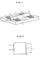
- Fig. 1 is a perspective view showing a mounted state of a stress impedance effect element according to an embodiment of the present invention.
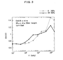
- Fig. 2 shows a high-sensitivity stress detection element according to the present invention and a circuit including it.
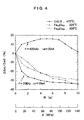
- Fig. 3 is a frequency characteristic (1) of the variation in voltage amplitude by the stress, of the high-sensitivity stress detection element according to the present invention.
- Fig. 4 is a frequency characteristic (2) of the variation in voltage amplitude by the stress, of the high-sensitivity stress detection element according to the present invention.
- Fig. 2 shows a high-sensitivity stress detection element according to the present invention and a circuit including it; and Fig. 3 shows a frequency characteristic (1) of the variation in voltage amplitude by the stress, of the high-sensitivity stress detection element.
- a sine-wave alternating current power supply 12 is connected to this amorphous wire 11.
- Reference numeral 13 denotes an internal resistor for maintaining constant the amplitude of the alternating current.
- Fig. 3 shows measured results of amplitudes Em of voltages occurring across the opposite ends of the amorphous wire 11 when a tensile force is applied to the amorphous wire 11, and sine-wave alternating currents having frequencies f and an amplitude of 15 mA are applied to the amorphous wire 11 by the sine-wave alternating current power supply 12.
- the application of a tensile force F of approximately 6 kg/mm 2 (60 MPa) to the amorphous wire 11 increases the amplitude Em of voltage across the opposite ends of the amorphous wire 11 in the range of frequency f from 50 kHz to 1 MHz, and reduces it in the frequency range from 1 MHz to about 20 MHz. In the range over 50 kHz, the amplitude Em of voltage across the opposite ends of the amorphous wire 11 increases with the frequency f. This shows an appearance of the skin effect in the amorphous wire 11.
- Fig. 4 shows a frequency characteristic (2) of the variation in voltage amplitude by the stress at frequencies of 400 kHz and 20 MHz, of the above-described high-sensitivity stress detection element.
- the measured results are of rates of the change in the amplitude Em of voltage across the opposite ends of these wires.
- the application of a load of 1 g reduces the amplitude Em of voltage across the opposite ends of these wires by 20%.
- the CoSiB amorphous wire has a maximum tensile strength of 306 MPa and maximum strain (elongation rate) of 3.4%
- its strain gauge factor [(rate of the change in electromagnetic quantity)/(elongation rate)] becomes 1286. This is a very high value about 6.5 times the gauge factor of about 200 owned by a conventional semiconductor strain gauge having a highest sensitivity.
- Even the FeCoSiB wire exhibits a gauge factor of about 400; this shows that a thin amorphous wire subjected to wire tension annealing exhibits a very high gauge factor.
- Fig. 1 is a perspective view showing a mounted state of the stress impedance effect element according to the embodiment of the present invention.
- reference numeral 1 denotes a glass ceramic substrate having a thermal expansion coefficient equal to that of an amorphous wire
- numeral 2 denotes the amorphous wire (magnetostrictive amorphous wire)
- 3 denotes a groove formed in the glass ceramic substrate 1
- 4 denotes electrodes formed across the groove 3 and comprising a Cu or NiFe film
- 5 denotes an insulating adhesive to be applied on the magnetostrictive amorphous wire 2.
- an amorphous wire (magnetostrictive amorphous wire) especially a negative magnetostrictive amorphous wire that has a diameter of not more than 20 ⁇ m can be used.
- the connection between electrodes 4 and the opposite end portions 2A of the magnetostrictive amorphous wire 2 is established by ultrasonic bonding.
- the formation of the electrodes is performed by ultrasonic bonding in which an electroless plating film or electroless nickel plating film is provided as a primary plating.
- the amorphous wire is a hard and stiff elastic body with a Vickers hardness of about 1000 and has a silicon oxide film as a surface layer
- this embodiment allows a reliable formation of electrodes by using ultrasonic bonding.
- the substrate has a thermal expansion coefficient equal to that of the amorphous wire, there is no risk of the amorphous wire falling off the substrate.
- the stress impedance effect element constitutes an acceleration sensor
- the substrate and the amorphous wire has conventionally made line contact with each other, the bonding therebetween has been imperfect.
- the amorphous wire 2 and the groove 3 are caused to make surface contact with each other by forming the groove 3 in the substrate 1, thereby allowing the amorphous wire 2 to be stably held.
- the magnetostrictive amorphous thin wire can be reliably mounted.
- the magnetostrictive amorphous thin wire is reliably connected to the electrodes by ultrasonic bonding.
- the magnetostrictive amorphous thin wire can also stably held to the groove formed in the substrate, and can be reliably fixed thereto by the insulating adhesive.
- the magnetostrictive amorphous thin wire can be fixed to the substrate stably and rigidly, thereby providing an impedance effect element that is resistant to an impactive force.
- the method for producing a stress impedance effect element, and that element according to the present invention can be expected to be widely used for a high-sensitivity dynamic quantity sensor based on the stress impedance effect.
Landscapes
- Physics & Mathematics (AREA)
- General Physics & Mathematics (AREA)
- Hall/Mr Elements (AREA)
- Pressure Sensors (AREA)
- Measuring Fluid Pressure (AREA)
Abstract
A method for producing a stress impedance effect element that can be rigidly mounted, and that element are provided. The stress impedance effect element has electrodes (4) each formed at a respective one of the opposite ends of a magnetostrictive amorphous thin wire (2), by ultrasonic bonding.
Description
- The present invention relates to a dynamic quantity sensor such as a strain gauge, stress sensor, accelerator sensor, and more specifically, to a high-sensitivity dynamic quantity sensor based on the stress impedance effect and its applications.
- For conventional strain gauges, resistance wire strain gauges and semiconductor strain gauges are in widespread practice, and the gauge factor (the rate of change of an impedance per unit strain) is about 2 for resistance wire strain gauges, and about 150 for semiconductor gauges.
- However, these gauge factor values are difficult to implement detection sensors for detecting minute strains and acceleration required for bioinstrumentation and high-accuracy industrial instrumentation. Strain gauges (stress sensors) having higher gauge factors must be developed.
- With this being the situation, the present inventor previously invented a high-sensitivity strain gauge (stress impedance effect element) based on the stress impedance effect of a magnetostrictive amorphous wire (Japanese Unexamined Patent Application Publication No. 10-170355). This stress impedance effect element has achieved a gauge factor of 4000 using a CoSiB amorphous wire with a diameter of 20 µm, thereby allowing the detection of minute strain, stress, acceleration, and the like.
- However, because the amorphous wire is a hard and stiff elastic body with a Vickers hardness of about 1000 and has a silicon oxide film as its surface layer, the formation of electrodes by soldering has been difficult. Also, when the stress impedance effect element constitutes an acceleration sensor, because its substrate and the amorphous wire make line contact with each other, the bonding therebetween has been imperfect. These problems have made difficult the mounting of the stress impedance effect element.
- Accordingly, the object of the present invention is to provide a method for producing a stress impedance effect element that can be rigidly mounted, and that element.
- In order to achieve the above-described object, the present invention provides:
- [1] a method for producing a stress impedance effect element, the method comprising connecting opposite ends of a magnetostrictive amorphous thin wire and respective electrodes by ultrasonic bonding;
- [2] the method for producing a stress impedance effect element as recited in the above [1], wherein the magnetostrictive amorphous thin wire is a negative magnetostrictive amorphous thin wire;
- [3] the method for producing a stress impedance effect element as recited in the above [1], wherein the magnetostrictive amorphous thin wire has a diameter of not more than 20 micrometers;
- [4] the method for producing a stress impedance effect element as recited in the above [1], the method comprising:
- forming a groove in an elastic thin substrate having a thermal expansion coefficient equal to that of the magnetostrictive amorphous thin wire; and
- installing the magnetostrictive amorphous thin wire in the groove, and bonding the magnetostrictive amorphous thin wire to the groove;
- [5] a stress impedance effect element comprising electrodes each formed at a respective one of the opposite ends of a magnetostrictive amorphous thin wire, by ultrasonic bonding;
- [6] the stress impedance effect element as recited in the above [5], wherein the magnetostrictive amorphous thin wire comprises a negative magnetostrictive amorphous thin wire;
- [7] the stress impedance effect element as recited in the above [5], wherein the magnetostrictive amorphous thin wire has a diameter of not more than 20 micrometers; and
- [8] the stress impedance effect element as recited in [5], wherein a groove is formed in an elastic thin substrate having a thermal expansion coefficient equal to that of the magnetostrictive amorphous thin wire, and wherein the magnetostrictive amorphous thin wire is installed in the groove and bonded to the groove.
- Fig. 1 is a perspective view showing a mounted state of a stress impedance effect element according to an embodiment of the present invention.
- Fig. 2 shows a high-sensitivity stress detection element according to the present invention and a circuit including it.
- Fig. 3 is a frequency characteristic (1) of the variation in voltage amplitude by the stress, of the high-sensitivity stress detection element according to the present invention.
- Fig. 4 is a frequency characteristic (2) of the variation in voltage amplitude by the stress, of the high-sensitivity stress detection element according to the present invention.
- Hereinafter, an embodiment according to the present invention will be described in detail.
- Fig. 2 shows a high-sensitivity stress detection element according to the present invention and a circuit including it; and Fig. 3 shows a frequency characteristic (1) of the variation in voltage amplitude by the stress, of the high-sensitivity stress detection element.
- In Fig. 2,
reference numeral 11 denotes a negative magnetostrictive amorphous wire comprising Co72.5Si12.5B15 (diameter=30 µm, length=20 mm; this amorphous wire is obtained by: drawing an amorphous wire with a diameter of 130 µm made by a rotation underwater rapid quenching method, and after heating it at 475°C for 2 min with a tensile force of 4 kg/mm2 applied, quenching it to room temperature; magnetostriction value= -3 × 10⁻⁶). A sine-wave alternatingcurrent power supply 12 is connected to thisamorphous wire 11.Reference numeral 13 denotes an internal resistor for maintaining constant the amplitude of the alternating current. - Fig. 3 shows measured results of amplitudes Em of voltages occurring across the opposite ends of the
amorphous wire 11 when a tensile force is applied to theamorphous wire 11, and sine-wave alternating currents having frequencies f and an amplitude of 15 mA are applied to theamorphous wire 11 by the sine-wave alternatingcurrent power supply 12. - As can be seen from Fig. 3, the application of a tensile force F of approximately 6 kg/mm2 (60 MPa) to the
amorphous wire 11 increases the amplitude Em of voltage across the opposite ends of theamorphous wire 11 in the range of frequency f from 50 kHz to 1 MHz, and reduces it in the frequency range from 1 MHz to about 20 MHz. In the range over 50 kHz, the amplitude Em of voltage across the opposite ends of theamorphous wire 11 increases with the frequency f. This shows an appearance of the skin effect in theamorphous wire 11. - Fig. 4 shows a frequency characteristic (2) of the variation in voltage amplitude by the stress at frequencies of 400 kHz and 20 MHz, of the above-described high-sensitivity stress detection element.
- In this embodiment, sine-wave alternating currents having frequencies of 400 kHz and 20 MHz and an amplitude of 20 mA is applied, and a tensile load W is provided to the CoSiB amorphous wire shown in Fig. 3 and a positive magnetostrictive amorphous wire comprising (Fe0.5 Co0.5)72.5 Si12.5B15 (diameter=30 µm, length=20 mm, magnetostriction value= 5 × 10⁻⁶). The measured results are of rates of the change in the amplitude Em of voltage across the opposite ends of these wires.
- For f=20 MHz, with the CoSiB wire, the application of a load of 1 g (tensile force=13 MPa) reduces the amplitude Em of voltage across the opposite ends of these wires by 20%. Because the CoSiB amorphous wire has a maximum tensile strength of 306 MPa and maximum strain (elongation rate) of 3.4%, its strain gauge factor [(rate of the change in electromagnetic quantity)/(elongation rate)] becomes 1286. This is a very high value about 6.5 times the gauge factor of about 200 owned by a conventional semiconductor strain gauge having a highest sensitivity. Even the FeCoSiB wire exhibits a gauge factor of about 400; this shows that a thin amorphous wire subjected to wire tension annealing exhibits a very high gauge factor.
- Hereinafter, characteristics of the present invention will be described.
- Fig. 1 is a perspective view showing a mounted state of the stress impedance effect element according to the embodiment of the present invention.
- In Fig. 1,
reference numeral 1 denotes a glass ceramic substrate having a thermal expansion coefficient equal to that of an amorphous wire,numeral 2 denotes the amorphous wire (magnetostrictive amorphous wire), 3 denotes a groove formed in the glassceramic substrate groove 3 and comprising a Cu or NiFe film, and 5 denotes an insulating adhesive to be applied on the magnetostrictiveamorphous wire 2. In this embodiment, an amorphous wire (magnetostrictive amorphous wire), especially a negative magnetostrictive amorphous wire that has a diameter of not more than 20 µm can be used. - In this embodiment, the connection between
electrodes 4 and the opposite end portions 2A of the magnetostrictiveamorphous wire 2 is established by ultrasonic bonding. Specifically, the formation of the electrodes is performed by ultrasonic bonding in which an electroless plating film or electroless nickel plating film is provided as a primary plating. - Although the formation of electrodes by soldering has been difficult because the amorphous wire is a hard and stiff elastic body with a Vickers hardness of about 1000 and has a silicon oxide film as a surface layer, this embodiment allows a reliable formation of electrodes by using ultrasonic bonding.
- Also, since the substrate has a thermal expansion coefficient equal to that of the amorphous wire, there is no risk of the amorphous wire falling off the substrate.
- Furthermore, when the stress impedance effect element constitutes an acceleration sensor, because the substrate and the amorphous wire has conventionally made line contact with each other, the bonding therebetween has been imperfect. However, in this embodiment, the
amorphous wire 2 and thegroove 3 are caused to make surface contact with each other by forming thegroove 3 in thesubstrate 1, thereby allowing theamorphous wire 2 to be stably held. - Moreover, since the
amorphous wire 2 is fixed by theinsulating adhesive 5, rigid mounting can be achieved. - The present invention is not limited to the above-described embodiment. Various modifications may be made therein on the basis of the true spirit of the present invention, and these modifications are not excluded from the scope of the present invention.
- As described above in detail, according to the present invention, the magnetostrictive amorphous thin wire can be reliably mounted. In other words, the magnetostrictive amorphous thin wire is reliably connected to the electrodes by ultrasonic bonding. The magnetostrictive amorphous thin wire can also stably held to the groove formed in the substrate, and can be reliably fixed thereto by the insulating adhesive.
- Thus, the magnetostrictive amorphous thin wire can be fixed to the substrate stably and rigidly, thereby providing an impedance effect element that is resistant to an impactive force.
- The method for producing a stress impedance effect element, and that element according to the present invention can be expected to be widely used for a high-sensitivity dynamic quantity sensor based on the stress impedance effect.
Claims (8)
- A method for producing a stress impedance effect element, the method comprising connecting opposite ends of a magnetostrictive amorphous thin wire and respective electrodes by ultrasonic bonding.
- The method for producing a stress impedance effect element according Claim 1, wherein the magnetostrictive amorphous thin wire is a negative magnetostrictive amorphous thin wire.
- The method for producing a stress impedance effect element according Claim 1, wherein the magnetostrictive amorphous thin wire has a diameter of not more than 20 micrometers.
- The method for producing a stress impedance effect element according Claim 1, the method comprising:forming a groove in an elastic thin substrate having a thermal expansion coefficient equal to that of the magnetostrictive amorphous thin wire; andinstalling the magnetostrictive amorphous thin wire in the groove, and bonding the magnetostrictive amorphous thin wire to the groove.
- A stress impedance effect element comprising electrodes each formed at a respective one of the opposite ends of a magnetostrictive amorphous thin wire, by ultrasonic bonding.
- The stress impedance effect element according Claim 5, wherein the magnetostrictive amorphous thin wire comprises a negative magnetostrictive amorphous thin wire.
- The stress impedance effect element according Claim 5, wherein the magnetostrictive amorphous thin wire has a diameter of not more than 20 micrometers.
- The stress impedance effect element according Claim 5, wherein a groove is formed in an elastic thin substrate having a thermal expansion coefficient equal to that of the magnetostrictive amorphous thin wire, and wherein the magnetostrictive amorphous thin wire is installed in the groove and bonded to the groove.
Applications Claiming Priority (3)
| Application Number | Priority Date | Filing Date | Title |
|---|---|---|---|
| JP2002096710A JP2003294548A (en) | 2002-03-29 | 2002-03-29 | Method for manufacturing stress impedance effect element and element thereof |
| JP2002096710 | 2002-03-29 | ||
| PCT/JP2003/003826 WO2003083423A1 (en) | 2002-03-29 | 2003-03-27 | Method for producing stress impedance effect element and that element |
Publications (2)
| Publication Number | Publication Date |
|---|---|
| EP1491870A1 true EP1491870A1 (en) | 2004-12-29 |
| EP1491870A4 EP1491870A4 (en) | 2007-07-18 |
Family
ID=28671845
Family Applications (1)
| Application Number | Title | Priority Date | Filing Date |
|---|---|---|---|
| EP03715505A Withdrawn EP1491870A4 (en) | 2002-03-29 | 2003-03-27 | PROCESS FOR PRODUCING AN EFFECTANCE ELEMENT BY STRESS AND ITEM |
Country Status (5)
| Country | Link |
|---|---|
| US (1) | US7318352B2 (en) |
| EP (1) | EP1491870A4 (en) |
| JP (1) | JP2003294548A (en) |
| CN (1) | CN1310019C (en) |
| WO (1) | WO2003083423A1 (en) |
Families Citing this family (9)
| Publication number | Priority date | Publication date | Assignee | Title |
|---|---|---|---|---|
| US9074860B2 (en) | 2013-03-13 | 2015-07-07 | Ametek | Systems and methods for magnetostrictive sensing |
| JP6325482B2 (en) * | 2015-04-06 | 2018-05-16 | バンドー化学株式会社 | Capacitance type sensor sheet and sensor device |
| JP6405497B1 (en) | 2015-08-31 | 2018-10-17 | コーニンクレッカ フィリップス エヌ ヴェKoninklijke Philips N.V. | Electroactive polymer sensor and detection method |
| CN111856354B (en) * | 2019-04-26 | 2024-01-19 | 中国科学院宁波材料技术与工程研究所 | Magnetic sensor with both wide measuring range and high sensitivity, its preparation method and use method |
| JP6830585B1 (en) * | 2019-08-15 | 2021-02-17 | ナノコイル株式会社 | Stress impedance sensor element and stress impedance sensor |
| JP6869496B1 (en) * | 2020-12-07 | 2021-05-12 | マグネデザイン株式会社 | Stylus bar with stress impedance element and stylus sensor |
| US11719768B2 (en) * | 2021-03-24 | 2023-08-08 | Showa Denko K.K. | Magnetic sensor and magnetic sensor device |
| CN114061435B (en) * | 2021-11-15 | 2024-07-26 | 无锡纤发新材料科技有限公司 | Micro-strain sensor based on magnetic fiber and strain monitoring method |
| CN114061434A (en) * | 2021-11-15 | 2022-02-18 | 浙江大学 | Structural health monitoring system and method for magnetic fiber composite material |
Family Cites Families (17)
| Publication number | Priority date | Publication date | Assignee | Title |
|---|---|---|---|---|
| US3465306A (en) * | 1964-06-01 | 1969-09-02 | Richard L Snyder | Oriented magnetic memory cores |
| US4894615A (en) * | 1986-03-03 | 1990-01-16 | Geo-Centers, Inc. | Stress-relieved amorphous metal ribbon magnetometer having viscous fluid interface |
| US5201964A (en) * | 1989-06-21 | 1993-04-13 | The United States Of America As Represented By The Secretary Of The Navy | Magnetostrictive torque sensor |
| DE4309413C2 (en) * | 1993-03-19 | 1996-03-07 | Holger Kabelitz | Magnetoelastic strain measuring unit for the detection of strains on a component surface |
| JPH06288844A (en) * | 1993-03-31 | 1994-10-18 | Matsushita Electric Ind Co Ltd | Mechanical quantity sensor |
| US5889403A (en) * | 1995-03-31 | 1999-03-30 | Canon Denshi Kabushiki Kaisha | Magnetic detecting element utilizing magnetic impedance effect |
| US5600239A (en) * | 1995-06-16 | 1997-02-04 | The United States Of America As Represented By The Secretary Of The Navy | Strain sensing system including a magnetostrictive material having a piezomagnetic property selected for maximizing electrical impedance to current applied to a predetermined skin depth |
| JP3614588B2 (en) * | 1996-12-06 | 2005-01-26 | 独立行政法人科学技術振興機構 | High sensitivity stress detector |
| US6231968B1 (en) * | 1997-09-04 | 2001-05-15 | Matsushita Electric Industrial Co., Ltd. | Magnetic thin film and magnetic device using the same |
| JP2000081471A (en) | 1998-06-30 | 2000-03-21 | Aichi Steel Works Ltd | Magnetic impedance element and magnetic impedance sensor excellent in thermal shock and mechanical vibration |
| US6472868B1 (en) * | 1998-08-05 | 2002-10-29 | Minebea Co., Ltd. | Magnetic impedance element having at least two thin film-magnetic cores |
| JP2001116814A (en) * | 1999-10-22 | 2001-04-27 | Canon Electronics Inc | Magnetic impedance element |
| JP2001296127A (en) * | 2000-04-13 | 2001-10-26 | Aichi Steel Works Ltd | Magnetic field detector |
| JP2002081471A (en) * | 2000-09-04 | 2002-03-22 | Honda Motor Co Ltd | Clutch control device for hybrid vehicle |
| JP3751514B2 (en) * | 2000-09-08 | 2006-03-01 | 独立行政法人科学技術振興機構 | Brain machine diagram sensor |
| JP2002090432A (en) * | 2000-09-12 | 2002-03-27 | Aichi Steel Works Ltd | Magnetic field detector |
| JP4695325B2 (en) * | 2001-09-17 | 2011-06-08 | キヤノン電子株式会社 | Magnetic detection element, method of manufacturing the same, and portable device using the element |
-
2002
- 2002-03-29 JP JP2002096710A patent/JP2003294548A/en active Pending
-
2003
- 2003-03-27 EP EP03715505A patent/EP1491870A4/en not_active Withdrawn
- 2003-03-27 CN CNB038074699A patent/CN1310019C/en not_active Expired - Fee Related
- 2003-03-27 US US10/507,373 patent/US7318352B2/en not_active Expired - Fee Related
- 2003-03-27 WO PCT/JP2003/003826 patent/WO2003083423A1/en not_active Ceased
Also Published As
| Publication number | Publication date |
|---|---|
| WO2003083423A1 (en) | 2003-10-09 |
| JP2003294548A (en) | 2003-10-15 |
| US7318352B2 (en) | 2008-01-15 |
| EP1491870A4 (en) | 2007-07-18 |
| US20060225512A1 (en) | 2006-10-12 |
| CN1643356A (en) | 2005-07-20 |
| CN1310019C (en) | 2007-04-11 |
Similar Documents
| Publication | Publication Date | Title |
|---|---|---|
| US11740142B2 (en) | Piezoelectric thin-film sensor and use thereof | |
| EP0528279A1 (en) | Flexible piezoelectric device | |
| CN105657626B (en) | Capacitive micro-machined ultrasonic transducer and subject information acquisition apparatus comprising it | |
| US7318352B2 (en) | Method for producing stress impedance effect element and that element | |
| KR920010551B1 (en) | Distortion measuring method and distortion measuring device | |
| JPH06216422A (en) | Flexible laminated piezoelectric element | |
| US20220137086A1 (en) | Acceleration transducer | |
| EP0618628B1 (en) | Mechanical sensor | |
| JP2022074049A (en) | Acceleration transducer | |
| EP1571434B1 (en) | Strain detector and pressure sensor | |
| JP3706903B2 (en) | Flexible high sensitivity ceramic sensor | |
| CN115768994A (en) | Force sensing device, vehicle braking device including such a force sensing device, and production method thereof | |
| JP2006226858A (en) | Fluctuating load sensor and tactile sensor using the same | |
| JPH04315056A (en) | Acceleration sensor | |
| JP6679183B2 (en) | Piezoelectric sensor and device including piezoelectric sensor | |
| JP7027485B2 (en) | Contact force measuring device and contact force measuring method using contact force measuring device | |
| JP2000356505A (en) | Strain detection element | |
| EP0694785B1 (en) | Acceleration sensor | |
| KR20080023398A (en) | Force Sensor Using Silicon Nanowires and Manufacturing Method Thereof | |
| JP2003340371A (en) | Piezo actuator | |
| KR101647744B1 (en) | Manufacturing method of pulse sensor, and manufacturing method of pulse measuring device | |
| CN114061435B (en) | Micro-strain sensor based on magnetic fiber and strain monitoring method | |
| US20160061670A1 (en) | Load detector | |
| JP2002310812A (en) | High sensitivity strain gauge | |
| JPS62239800A (en) | Piezoelectric element |
Legal Events
| Date | Code | Title | Description |
|---|---|---|---|
| PUAI | Public reference made under article 153(3) epc to a published international application that has entered the european phase |
Free format text: ORIGINAL CODE: 0009012 |
|
| 17P | Request for examination filed |
Effective date: 20040928 |
|
| AK | Designated contracting states |
Kind code of ref document: A1 Designated state(s): AT BE BG CH CY CZ DE DK EE ES FI FR GB GR HU IE IT LI LU MC NL PT RO SE SI SK TR |
|
| A4 | Supplementary search report drawn up and despatched |
Effective date: 20070620 |
|
| STAA | Information on the status of an ep patent application or granted ep patent |
Free format text: STATUS: THE APPLICATION HAS BEEN WITHDRAWN |
|
| 18W | Application withdrawn |
Effective date: 20080128 |