EP1489706A1 - Optical module and method for assembling optical module - Google Patents
Optical module and method for assembling optical module Download PDFInfo
- Publication number
- EP1489706A1 EP1489706A1 EP03710340A EP03710340A EP1489706A1 EP 1489706 A1 EP1489706 A1 EP 1489706A1 EP 03710340 A EP03710340 A EP 03710340A EP 03710340 A EP03710340 A EP 03710340A EP 1489706 A1 EP1489706 A1 EP 1489706A1
- Authority
- EP
- European Patent Office
- Prior art keywords
- solder
- joining
- thermo
- control module
- optical
- Prior art date
- Legal status (The legal status is an assumption and is not a legal conclusion. Google has not performed a legal analysis and makes no representation as to the accuracy of the status listed.)
- Withdrawn
Links
Images


Classifications
-
- G—PHYSICS
- G02—OPTICS
- G02B—OPTICAL ELEMENTS, SYSTEMS OR APPARATUS
- G02B6/00—Light guides; Structural details of arrangements comprising light guides and other optical elements, e.g. couplings
- G02B6/24—Coupling light guides
- G02B6/42—Coupling light guides with opto-electronic elements
- G02B6/4201—Packages, e.g. shape, construction, internal or external details
- G02B6/4219—Mechanical fixtures for holding or positioning the elements relative to each other in the couplings; Alignment methods for the elements, e.g. measuring or observing methods especially used therefor
- G02B6/4236—Fixing or mounting methods of the aligned elements
- G02B6/4238—Soldering
-
- G—PHYSICS
- G02—OPTICS
- G02B—OPTICAL ELEMENTS, SYSTEMS OR APPARATUS
- G02B6/00—Light guides; Structural details of arrangements comprising light guides and other optical elements, e.g. couplings
- G02B6/24—Coupling light guides
- G02B6/42—Coupling light guides with opto-electronic elements
- G02B6/4201—Packages, e.g. shape, construction, internal or external details
-
- G—PHYSICS
- G02—OPTICS
- G02B—OPTICAL ELEMENTS, SYSTEMS OR APPARATUS
- G02B6/00—Light guides; Structural details of arrangements comprising light guides and other optical elements, e.g. couplings
- G02B6/24—Coupling light guides
- G02B6/42—Coupling light guides with opto-electronic elements
- G02B6/4201—Packages, e.g. shape, construction, internal or external details
- G02B6/4266—Thermal aspects, temperature control or temperature monitoring
- G02B6/4268—Cooling
- G02B6/4271—Cooling with thermo electric cooling
-
- H—ELECTRICITY
- H01—ELECTRIC ELEMENTS
- H01S—DEVICES USING THE PROCESS OF LIGHT AMPLIFICATION BY STIMULATED EMISSION OF RADIATION [LASER] TO AMPLIFY OR GENERATE LIGHT; DEVICES USING STIMULATED EMISSION OF ELECTROMAGNETIC RADIATION IN WAVE RANGES OTHER THAN OPTICAL
- H01S5/00—Semiconductor lasers
- H01S5/02—Structural details or components not essential to laser action
- H01S5/022—Mountings; Housings
- H01S5/023—Mount members, e.g. sub-mount members
- H01S5/02315—Support members, e.g. bases or carriers
-
- H—ELECTRICITY
- H01—ELECTRIC ELEMENTS
- H01S—DEVICES USING THE PROCESS OF LIGHT AMPLIFICATION BY STIMULATED EMISSION OF RADIATION [LASER] TO AMPLIFY OR GENERATE LIGHT; DEVICES USING STIMULATED EMISSION OF ELECTROMAGNETIC RADIATION IN WAVE RANGES OTHER THAN OPTICAL
- H01S5/00—Semiconductor lasers
- H01S5/02—Structural details or components not essential to laser action
- H01S5/022—Mountings; Housings
- H01S5/02208—Mountings; Housings characterised by the shape of the housings
- H01S5/02216—Butterfly-type, i.e. with electrode pins extending horizontally from the housings
-
- H—ELECTRICITY
- H01—ELECTRIC ELEMENTS
- H01S—DEVICES USING THE PROCESS OF LIGHT AMPLIFICATION BY STIMULATED EMISSION OF RADIATION [LASER] TO AMPLIFY OR GENERATE LIGHT; DEVICES USING STIMULATED EMISSION OF ELECTROMAGNETIC RADIATION IN WAVE RANGES OTHER THAN OPTICAL
- H01S5/00—Semiconductor lasers
- H01S5/02—Structural details or components not essential to laser action
- H01S5/022—Mountings; Housings
- H01S5/0225—Out-coupling of light
- H01S5/02251—Out-coupling of light using optical fibres
-
- H—ELECTRICITY
- H01—ELECTRIC ELEMENTS
- H01S—DEVICES USING THE PROCESS OF LIGHT AMPLIFICATION BY STIMULATED EMISSION OF RADIATION [LASER] TO AMPLIFY OR GENERATE LIGHT; DEVICES USING STIMULATED EMISSION OF ELECTROMAGNETIC RADIATION IN WAVE RANGES OTHER THAN OPTICAL
- H01S5/00—Semiconductor lasers
- H01S5/02—Structural details or components not essential to laser action
- H01S5/022—Mountings; Housings
- H01S5/023—Mount members, e.g. sub-mount members
- H01S5/02325—Mechanically integrated components on mount members or optical micro-benches
- H01S5/02326—Arrangements for relative positioning of laser diodes and optical components, e.g. grooves in the mount to fix optical fibres or lenses
-
- H—ELECTRICITY
- H01—ELECTRIC ELEMENTS
- H01S—DEVICES USING THE PROCESS OF LIGHT AMPLIFICATION BY STIMULATED EMISSION OF RADIATION [LASER] TO AMPLIFY OR GENERATE LIGHT; DEVICES USING STIMULATED EMISSION OF ELECTROMAGNETIC RADIATION IN WAVE RANGES OTHER THAN OPTICAL
- H01S5/00—Semiconductor lasers
- H01S5/02—Structural details or components not essential to laser action
- H01S5/022—Mountings; Housings
- H01S5/0233—Mounting configuration of laser chips
-
- H—ELECTRICITY
- H01—ELECTRIC ELEMENTS
- H01S—DEVICES USING THE PROCESS OF LIGHT AMPLIFICATION BY STIMULATED EMISSION OF RADIATION [LASER] TO AMPLIFY OR GENERATE LIGHT; DEVICES USING STIMULATED EMISSION OF ELECTROMAGNETIC RADIATION IN WAVE RANGES OTHER THAN OPTICAL
- H01S5/00—Semiconductor lasers
- H01S5/02—Structural details or components not essential to laser action
- H01S5/022—Mountings; Housings
- H01S5/0235—Method for mounting laser chips
Definitions
- the present invention relates to an optical module and a method of assembling the optical module, which have a good coupling efficiency with an optical fiber.
- Semiconductor laser modules (which have a semiconductor laser, etc.) are usually employed as signal light sources for optical fiber communications, particularly trunk lines and cable television (CATV), or as pumping sources for optical fiber pumps.
- such semiconductor laser modules have a semiconductor laser, a photodiode chip, optics such as a lens, a thermistor, etc., which are arranged at predetermined positions on a metal plate mounted on a thermo-control module capable of controlling temperature in dependence on the magnitude and direction of current conduction.
- Fig. 8 shows a conventional semiconductor lasermodule having a thermo-control module incorporated therein.
- the semiconductor laser module 101 has a thermo-control module 103 mounted on the bottom plate 102 of the package through a lower joining solder portion 110.
- the thermo-control module 103 has a metal plate 105 mounted thereon.
- the metal plate 105 is provided with a carrier substrate106, a semiconductor laser 107, a condensing lens 108, etc.
- the lower substrate 104a of thermo-control module 103 and the package bottom plate 102 are joined with the lower joining solder portion 110.
- the upper substrate 104b of the thermo-control module 103 and the metal plate 105 are joined with an upper joining solder portion 111.
- the lower substrate 104a of the thermo-control module 103 and the bottom plate 102 of the package are joined with solder consisting of an alloy of 63 wt% (weight-percent) Sn and 37 wt% Pb, and the lower joining solder portion 110 is formed.
- solder consisting of an alloy of 63 wt% (weight-percent) Sn and 37 wt% Pb, and the lower joining solder portion 110 is formed.
- Fig. 1C there is also a semiconductor laser module 1 having no internal thermo-control module.
- the conventional optical module has the following disadvantages. That is, when joining the thermo-control module 103 and the package bottom plate 102 with solder, load is applied while melting the solder, but since the way of applying this load is not constant, the joining solder portion 110 is not uniform in thickness, as shown in Fig. 8. If the joining solder portion 110 is not uniform in thickness, it will be deformed due to a change in the temperature of the environment where the optical module is used, or a change in temperature when manufacturing the optical module. This deformation causes, for example, positional misalignment between the optical component 108 and optical fiber 109 optically aligned through the joining solder portion 110. As shown by an alternate long and short dash line, an error occurs in the axial alignment between the optical component 108 and the optical fiber 109 and causes a reduction in a coupling efficiency with an optical fiber and degradation of light output.
- the above-described conventional optical module is shown in Japanese Laid-Open Publication Nos. 2000-323731, 2000-280090, Hei 7-128550, and Hei 11-295560.
- the present invention has been made in view of the above-described circumstances. Accordingly, it is the primary object of the invention to provide an optical module and an optical-module assembling method that use lead-free solder, suppress optical-axis misalignment by preventing deformation and cracks from occurring in solder portions, and have a good coupling efficiency with an optical fiber.
- thermo-control module and a package are joined with Sn-Ag solder or Sn-Zn solder, gold (Au) is diffused from the Au-plated layer formed on the package surface and the Au-plated layer on the surface of the bottom of the thermo-control module into Sn-Ag solder or Sn-Zn solder, and an approximately even phase is formed.
- Au gold
- thermo-control module becomes approximately constant and positioning of a metal plate mounting optical components thereon becomes easy.
- member misalignment due to the thermal expansion of solder is approximately constant, so optical-axis misalignment can be appreciably reduced compared with the above-described conventional optical module, and a reduction in light output can be suppressed.
- a first preferred form of the optical module of the present invention is an optical module comprising (1) at least one optical component; (2) a package for housing the aforementioned at least one optical component; and (3) a joining portion.
- the joining portion is formed within the package by Sn-Ag solder containing 2.0 to 5.0 wt%(weight-percent) Ag and further containing 2. 0 to 20. 0 wt% Au, or Sn-Zn solder containing 6.0 to 10.0 wt% Zn and further containing 2.0 to 20.0 wt% Au.
- a second preferred form of the optical module of the present invention is an optical module comprising (1) at least one optical component; (2) a thermo-control module for temperature-controlling the aforementioned at least one optical component; (3) a package for housing the aforementioned at least one optical component and the thermo-control module; and (4) a joining portion.
- the joining portion is formed between the thermo-control module and the package, by Sn-Ag solder containing 2.0 to 5.0 wt% Ag and further containing 2.0 to 20.0 wt% Au, or Sn-Zn solder containing 6.0 to 10.0 wt% Zn and further containing 2.0 to 20.0 wt% Au.
- a third preferred form of the optical module of the present invention is an optical module comprising (1) at least one optical component; (2) a thermo-control module for temperature-controlling the aforementioned at least one optical component; (3) a package for housing the aforementioned at least one optical component and the thermo-controlmodule; and (4) a joining portion.
- the joining portion is formed between the thermo-control module and a base plate having the aforementioned at least one optical component mounted thereon, by Sn-Bi solder containing 10.0 to 60.0 wt% Bi.
- the aforementioned Sn-Ag solder further contains 1.0 to 3.0 wt% Cu.
- the aforementioned Sn-Ag solder further contains 1.0 to 10.0 wt% Bi.
- the aforementioned Sn-Zn solder further contains 1.0 to 5.0 wt% Bi.
- the aforementioned at least one optical component includes a semiconductor laser.
- the aforementioned joining portion is 5 to 100 ⁇ m in thickness.
- a difference in thickness between a front end (a1) and rear end (a2) of the joining portion in a direction parallel to a light emitting direction (A1-A2) of the package is 90 ⁇ m or less
- a difference in thickness between one end (b1) and the other end (b2) of the joining portion in a direction (B1-B2) perpendicular to the light emitting direction (A1-A2) is 90 ⁇ m or less.
- the aforementioned joining portion has a gold (Au) diffused portion where Au is dispersed in the solder.
- the Au diffused portion is formed by diffusing Au from a gold (Au) plated layer of 1 to 5 ⁇ m in thickness previously formed in at least either a surface of the package joining with the thermo-control module or a surface of the thermo-control module joining with the package.
- the aforementioned Sn-Ag solder or Sn-Zn solder overflows from the joining portion between the thermo-control module and the package.
- An twelfth preferred form of the optical module of the present invention is an optical module comprising (1) a carrier substrate mounting a semiconductor laser thereon; (2) a base plate mounting the carrier substrate thereon through a first joining solder portion; (3) a thermo-control module mounting the base plate thereon through a second joining solder portion, controlling temperature of the semiconductor laser, and comprising a Peltier element and upper and lower insulating substrates joined through a third joining solder portion; and (4) a package mounting the thermo-control module thereon through a fourth joining solder portion.
- T1, T2, T3, and T4 are the melting points of the first, second, third, and fourth solder portions, T1 ⁇ T2, T3 ⁇ T4 ⁇ T2, T3 ⁇ 240°C, and 280°C ⁇ T4 ⁇ 190°C.
- solder forming the third joining solder portion is composed of 80 wt% Au and 20 wt% Sn.
- solder forming the third joining solder portion is a Bi-Sb alloy.
- a first preferred form of the optical-module assembling method of the present invention is an optical-module assembling method comprising:
- a second preferred form of the optical-module assembling method of the present invention is an optical-module assembling method comprising:
- the aforementioned solder joining step performs joining by employing Sn-Ag solder foil, the Sn-Ag solder foil being larger than the aforementioned one surface of the thermo-control module and also being 5 to 100 ⁇ m in thickness.
- the aforementioned solder joining step further includes a pretreatment step of removing an oxidized film on a surface of the Sn-Ag solder, before joining is performed by employing the Sn-Ag solder foil.
- the aforementioned solder joining step previously coats the aforementioned one surface of the thermo-control module with the Sn-Ag solder or the Sn-Zn solder.
- the aforementioned solder joining step includes a step of heating the Sn-Ag solder or the Sn-Zn solder so that the time it is melting is between 5 and 120 seconds.
- the aforementioned heating step presses the aforementioned one surface of the package and the aforementioned one surface of the thermo-control module against each other with a load of 3.0 ⁇ 10 4 Pa or less.
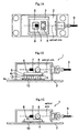
- the optical module 1 has a thermo-control module 3 mounted on the bottom plate 2 of the package through a lower joining solder portion 10.
- the thermo-control module 3 has a metal plate (baseplate) 5 mounted thereon.
- the metal plate 5 has a carrier substrate 6 and a condensing lens 8 mounted thereon.
- the carrier substrate 6 has a laser diode 7, a thermistor, etc., mounted thereon.
- the thermo-control module 3 consists of a lower insulating substrate 4a, a Peltier element 13, and an upper insulating substrate 4b.
- the lower insulating substrate 4a of the thermo-control module 3 and the bottom plate 2 of the package are joined with the lower joining solder portion 10.
- the upper insulating substrate 4b of the thermo-control module 3 and the metal plate 5 are joined with an upper joining solder portion 11.
- a preferred form of the optical module of the present invention is an optical module having at least one optical component and a package in which at least one optical component is packed.
- the optical module also has a joining portion formed from Sn-Ag solder consisting of 2.0 to 5.0 wt% Ag and Sn, or Sn-Zn solder consisting of 6.0 to 10.0 wt% Zn and Sn.
- optical module of the present invention is an optical module having at least one optical component, a thermo-control module for temperature-controlling at least one optical component, and a package in which at least one optical component and thermo-control module are packed.
- the optical module also has a joining portion, formed from Sn-Ag solder consisting of 2.0 to 5.0 wt% Ag and Sn or from Sn-Zn solder consisting of 6.0 to 10.0 wt% Zn and Sn, between the thermo-control module and the package.
- Sn-Ag solder and Sn-Zn solder are typically hard and they are difficult to deform.
- the joining of optical components employs Sn-Ag solder containing 2.0 to 5.0 wt% Ag, preferably 3.0 to 3.5 wt% Ag, or Sn-Zn solder containing 6.0 to 10.0 wt% Zn, preferably 8.5 wt% Zn. Therefore, the joining solder portions are not liable to undergo plastic deformation, so the joining solder portions are prevented from being deformed due to a change in the temperature of the environment where the optical module is used, or a change in temperature during manufacture of optical modules. It has been found that Sn-Ag solder and Sn-Zn solder is greater in tensile strength than conventional Sn-Pb solder. That is, they are not easily deformed plastically by mechanical strain produced due to a change in environment temperature.
- the above-described Sn-Ag solder may contain Cu of 3 wt% or less.
- Cu has the property of lowering the melting point of solder.
- the above-described Sn-Ag solder may further contain Bi of 10.0 wt% or less.
- the above-described Sn-Zn solder may contain Bi of 5.0 wt% or less. Bi has the property of enhancing wettability of solder.
- Cu has the property of lowering the melting point of solder
- Bi has the property of enhancing wettability ofsolder.
- Cu and Si are added to Sn-Ag solder, the wettability is enhanced and the occurrence of a void is suppressed.
- Bi is added to Sn-Zn solder, the wettability is enhanced.
- the above-described at least one optical component includes a semiconductor laser. Therefore, the optical axis of the semiconductor layer needs to be aligned with that of an optical fiber that is to be coupled with the optical module. In addition, the influence of optical-axis misalignment on module performance is great. Therefore, for instance, if a joining solder portion is not uniform in thickness by a change in temperature, optical-axis misalignment becomes greater and light output is reduced. Therefore, joining solder portions are also required to have high performance so optical-axis misalignment becomes smaller.
- the present invention is also applicable even when the semiconductor laser module 1 has no thermo-control module.
- the metal plate 5, which has the carrier substrate 6 and condensing lens 8 mounted thereon is mounted directly on the package bottom plate 2 with solder. That is, the joining solder portion 10 is formed between the metal plate 5 and the package bottom plate 2.
- the above-described joining solder portion i.e., solder portion
- the above-described joining solder portion is 5 to 100 ⁇ m in thickness. If the thickness of the joining solder portion is too thin (less than 5 ⁇ m), there is a possibility that mechanical stress due to deformation such as a warp in the package bottom plate will concentrate and therefore cracks will occur in the joining solder portion. On the other hand, if the thickness of the joining solder portion is too thick (great than 100 ⁇ m), it will be easily deformed plastically with small mechanical stress.
- the thickness of the joining portion needs to be limited to a range of 5 to 100 ⁇ m.
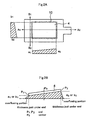
- Fig. 2 shows the thicknesses in predetermined directions of the joining solder portion.
- a direction in which light is emitted from the package is represented by (A1-A2)
- a direction perpendicular to the direction of (A1-A2) is represented as (B1-B2).
- the thicknesses of solder just under the front and rear ends of the thermo-control module substrate 4a in the direction of (A1-A2) are represented as a1 and a2.
- the thicknesses of solder just under both ends of the thermo-control module substrate 4a in the direction of (B1-B2) are represented as b1 (one end) and b2 (the other end).
- the solder thickness may be measured at positions determined from an arbitrary position on the package.
- the difference in thickness between the front end (a1) and rear end (a2) of the joining solder portion in the direction parallel to the light emitting direction (A1-A2) of the package is 90 ⁇ m or less, and/or the difference in thickness between one end (b1) and the other end (b2) of the joining solder portion in the direction (B1-B2) perpendicular to the light emitting direction (A1-A2) is 90 ⁇ m or less.
- the thickness of the joining solder portion may be the maximum value or minimum value in the direction (B1-B2) of a1 and a2 and in the direction (A1-A2) of b1 and b2, or may be an average value of arbitrarypoints. Note that the thickness of the joining solder portion may adopt the maximum value or minimum value measured between the lower substrate of thermo-control module and the package bottom surface, or may adopt an average value (see Fig. 2B).
- thermo-control module by respectively controlling the difference in thickness between the front end (a1) and rear end (a2) of the joining solder portion in the direction (A1-A2) and the difference in thickness between one end (b1) and the other end (b2) of the joining solder portion in the direction (B1-B2 ) to predetermined values or less, the thermo-control module can maintain approximately its position even at high temperature. Therefore, alignment of optical components mounted on the thermo-control module becomes easier and member misalignment due to the thermal expansion of the joining solder portion becomes constant even at high temperature. Thus, optical-axis misalignment can be suppressed and a reduction in light output can be minimized.
- the joining solder portion contains 2.0 to 10.0 wt% Au. That is, preferably, 2.0 to 20.0 wt% Au is further contained in Sn-Ag solder and Sn-Zn solder. If the respective solders contain Au, compounds of Au and Sn (Sn 4 Au, etc.) are evenly dispersed and the ductility of the joining solder portion becomes smaller, so creep deformation due to thermal stress can be prevented. If Au is less than 2.0 wt%, there is a problem that advantages by a reduction in the ductility cannot be sufficiently obtained. Also, if Au exceeds 2.0 wt%, the melting point of solder rises sharply and solidification occurs at a portion whose melting point has risen, so there is a problem that alignment operation will become worse.
- the joining solder portion is equipped with an Au-diffused portion where Au is dispersed in solder.
- the Au-diffused portion is formed by diffusing Au from an Au-plated layer of 1 to 5 ⁇ m in thickness previously formed in at least either the joining surface of the package with the thermo-control module or the joining surface of the thermo-control module with the package.
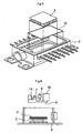
- Fig. 3 shows a joining solder portion equipped with an Au-diffused portion where Au is dispersed in solder.
- the case of Sn-Ag solder is shown in Fig. 3A.
- the case of Sn-Zn solder is shown in Fig. 3B, and the case of conventional Sn-Pb solder is shown in Fig. 3C.
- Au-Sn compounds (Sn 4 Au, etc.) are diffused from Au-plated layers formed on the lower substrate of the thermo-control module and the bottom surface of the package and are evenly dispersed in a Sn-Ag alloy phase.
- structures (Sn 4 Au, etc.)of about 5 to 10 ⁇ m in diameter are evenly dispersed and an even phase is formed as the entirety of the joining solder portion.
- Au-Sn compounds are diffused from Au-plated layers formed on the lower substrate of the thermo-control module and the bottom surface of the package and are evenly dispersed in a Sn-Ag alloy phase.
- the Pb-rich phases in the central portion deform with weak mechanical stress, so the joining solder portion is prone to creep.
- Au is evenly dispersed and enhances mechanical strength, so creeping is suppressed and optical-axis misalignment is not prone to occur.
- Au is evenly dispersed and enhances mechanical strength, so creeping is suppressed and optical-axis misalignment is less prone to occur.
- the amount of Au diffusion into the solder alloy may be reduced.
- the amount of Au diffusion into the solder alloy may be reduced, if at least one of the two Au-plated layers, formed on the bottom surface of the metal plate and the top surface of the thermo-control module, is thin (0.01 to 1 ⁇ m), or if at least the Au-plated layer on the bottom surface of the metal plate is eliminated.
- optical-module assembling method of the present invention has:
- Fig. 4 shows the relationship between the lower substrate of the thermo-control module, solder, and the bottom surface of the package.
- the package has at least a Ni layer formed on the bottom surface consisting of 20 wt% Cu and 80 wt% W.
- the Ni layer has an Au layer of 1.5 to 2.0 ⁇ m in thickness formed on the surface thereof.
- the lower substrate of the thermo-control module has at least a Ni layer formed on alumina (Al 2 O 3 ) or aluminum nitride (AlN).
- the Ni layer has an Au layer of 0.3 ⁇ m in thickness formed on the surface thereof.
- the lower substrate of the thermo-control module and the bottom surface of the package are arranged so the respective Au layers face each other. Between them, there is arranged solder foil of 50 to 80 ⁇ m in thickness.
- a joining solder portion containing Au if at least either a surface of the package to be joined to the thermo-control module or a surface of the thermo-control module to be joined to the package has an Au layer of 1 to 5 ⁇ m in thickness, Au can diffuse from the Au-plated layer into Sn-Ag solder or Sn-Zn solder when they are joined with the solder. If the joining surface is coated with an Au layer, the oxidization of a surface to be joined can be suppressed and the manufacturing step is simplified compared with the case where a solder alloy containing Au is employed. In addition, since solder containing Au from the beginning increases its mechanical strength, it is fairly difficult to roll the solder into foil. Thus, the assembling method of the present invention is capable of simplifying the manufacturing step and equipment.
- the thickness of the Au layer is less than 1 ⁇ m, ductility is not sufficiently reduced. Also, if the thickness of the Au layer exceeds 5 ⁇ m, an excessive rise in the melting point due to coupling of molten solder alloy and Au cannot be prevented.
- the above-described solder joining step employs Sn-Ag solder foil to perform joining.
- the Sn-Ag solder foil is larger than a surface of the thermo-control module having the Au-plated layer formed thereon, and is 5 to 100 ⁇ m in thickness.
- solder is diffused along the Au-plated layer, so the thickness of the solder layer is prevented from varying significantly.
- positional misalignment is negligible in mounting the thermo-control module on the package bottom surface.
- the solder thickness is within a range of 5 to 100 ⁇ m, cracks due to thermal stress are suppressed and creep deformation can be minimized.
- the above-described solder joining step further includes the step of processing the surface of Sn-Ag solder foil before joining is performed with the Sn-Ag solder foil. For example, by etching the surface of the Sn-Ag solder foil with an acid, an oxidized film on the solder surface can be removed, so wettability of the solder can be enhanced.
- the etching process is not limited to acids.
- the oxidized film may be removed by chemical dry etching, mechanical polishing, etc.
- the above-described solder joining step performs joining by previously coating a surface of the thermo-control module, which has an Au layer, with Sn-Ag solder or Sn-Zn solder.
- thermo-control module if the Au-plated layer is coated with solder, it becomes unnecessary to apply solder when joining. All that is required is to arrange the thermo-control module at a predetermined position, so the time and labor required for placing solder foil at a predetermined position can be saved.
- the above-described solder joining step includes the step of heating Sn-Ag solder or Sn-Zn solder so that the time it is melting is between 5 and 120 seconds.
- the time solder is melting is less 5 seconds, Au plating does not melt sufficiently into the solder. Also, if the time solder is melting exceeds 120 seconds, molten solder cannot be prevented from advancing rapidly along the bottom surface of the package. That is, if the time solder is melting is too long, the solder and the gold plating on the bottom surface are alloyed and a deviation in melting point occurs. As a result, solidification occurs at a portion whose melting point is higher, and for example, a void is formed. Generally it is preferred to make the melting time of solder shorter. Preferably, the time solder is melting is 60 seconds or less.
- the above-described heating step presses the Au-plated surface of the package and the Au-plated surface of the thermo-control module against each other with a load of 3.0 ⁇ 10 4 Pa or less.
- the solder foil supplied in the solder joining step is pressed with a load of 3.0 ⁇ 10 4 Pa or less and is heated. In this state, solder joining is performed while solder is being melted. Therefore, solder can be prevented from spreading out irregularly along a surface to be joined, when heated and pressed.
- the thickness of the Sn-Ag solder or Sn-Zn solder in a joining solder portion can be made approximately the same as solder foil supplied or solder previously coated. Thus, the thickness of solder can be easily controlled. In addition, it can be easily made uniform.
- the optical module of the present invention is equipped with (1) a carrier substrate mounting a semiconductor laser thereon; (2) a base plate mounting the carrier substrate thereon through a first joining solder portion (A); (3) a thermo-control module mounting the base plate thereon through a second joining solder portion (B), controlling temperature of the semiconductor laser, and consisting of a Peltier element and upper and lower insulating substrates joined through a third joining solder portion (C); and (4) a package mounting the thermo-control module on a bottom surface thereof through a fourth joining solder portion (D).
- the melting points of the solder portions (A), (B), (C), and (D) are T1, T2, T3, and T4, T1 ⁇ T2 and T3 ⁇ T4 ⁇ T2.
- the melting point of the third solder portion (C) is T3 ⁇ 240°C, and the melting point of the fourth solder portion (D) is 280°C ⁇ T4 ⁇ 190°C.
- the solder forming the third joining solder portion (C) may be composed of 80 wt% Au and 20 wt% Sn.
- the solder forming the third joining solder portion (C) may also be a Bi-Sb alloy.
- the melting point of the solder within the thermo-control module is made higher. Therefore, the melting point of the solder for joining the thermo-control module and the package can be made higher. As a result, optical-axis misalignment due to a change in temperature is significantly reduced. And durability at high temperature is significantly enhanced, so reliability can be enhanced.
- optical module and the optical-module assembling method of the present invention will hereinafter be described in detail with reference to embodiments.
- thermo-control module with a substrate of size 8 mm ⁇ 8 mm and thickness 2 mm, were prepared.
- the substrate surface of the thermo-control module was plated with Au of thickness 0.2 ⁇ m.
- a solder palette 10 (also called solder foil) with a size of 12 mm ⁇ 8 mm ⁇ 0.05 mm was used. It consists of Sn - 0.3 wt% Ag - 0.5 wt% Cu. With the Au-plated surfaces arranged to face each other, the package 2 and the thermo-control module were joined as follows.
- the solder palette 10 was immersed in hydraulic acid of 3% concentration for 10 minutes, and after removal of the oxidized film on the solder surface, it was washed in water. Thereafter, the package 2 was placed on a stage, the solder foil 10 was mounted on the central portion of the bottom plate of the package 2, and the thermo-control module 3 was stacked on the solder foil 10. Furthermore, a positioning jig with a weight of 5g was placed on the top of the thermo-control module 3 in order to prevent the thermo-control module 3 from being moved greatly by solder when melted. (At this time, the load applied to the solder by the positioning jig of weight 5g was 7.7 ⁇ 10 2 Pa. That is, since the weight of the jig is a predetermined value or less, the surface tension of the solder can maintain its original thickness, even when the solder is melted.)
- the package 2 on the stage was heated.
- the peak temperature of the stage was set to 225°C, and the stage temperature was controlled so the time Sn-Ag-Cu solder is melting at the melting portion 217°C or greater was 20 seconds. Since the melting time of the solder is short (20 seconds) and the thickness of the gold-plated film on the bottom plate of the package is thick (1.5 ⁇ m), the overflow of melted solder to the package bottom surface can be made very small. For that reason, the solder thickness of the joining solder portion is approximately the same as the original thickness of the solder palette 10. The thickness was 40 to 50 ⁇ m. (If the melting time is long, the amount that the solder overflows out is increased. Because of this, the solder is not uniform in thickness and a void is apt to occur.)
- the atmosphere is inert gas such as nitrogen, etc., or mixed gas, etc., and contains oxygen as little as possible.
- the gold plating in the package bottom surface and the gold plating in the thermo-control module have been molten into that solder portion.
- the gold content of the joining solder portion is about 8.0%.
- the ductility of the solder portion itself is reduced, so creep deformation due to thermal stress is difficult to occur.
- thermo-control module with solder. More specifically, Sn-Bi solder palette 11 was placed on the top surface of the thermo-control module 3, the base plate 5 was positioned, the package 2 was heated up to 175°C, the solder palette 11 was melted, and the base plate 5 was joined to thermo-control module 3.
- an optical fiber was attached to the package, and the laser beam from the package was optically aligned with the axis of the optical fiber. In this way, an optical module was completed.
- the optical module of the present invention thus assembled underwent a temperature cycle test (which repeats -40°C to 85°C) and a high-temperature shelf test (85°C).
- a temperature cycle test which repeats -40°C to 85°C
- a high-temperature shelf test 85°C
- the degradation of the light output after 1000 cycles in the case of conventional Sn-Pb solder is an average of 8%
- the degradation of the light output after 1000 cycles in the case of the present invention is an average of 4%.
- optical-axis misalignment due to a change in temperature is considerably reduced.
- the substrate of a thermo-control module was previously coated.
- the thermo-control module the Peltier element and upper and lower insulating substrates were joined with solder consisting of 80 wt% Au and 20 wt% Sn.
- the top surface (cooling surface) of the thermo-control module was previously coated with solder consisting of Sn, 57 wt% Bi, and 1. 0 wt% Ag, and the thickness was 100 ⁇ m at the central portion.
- the bottom surface (heating surface) of the thermo-control module was previously coated with solder consisting of Sn, 7.5 wt% Zn, and 3.0 wt% Bi, and the thickness was 100 ⁇ m at the central portion. While the thermo-control module was being heated on a hot plate, a predetermined amount of solder was melted with a soldering iron, and the substrate was first coated with Sn-Zn-Bi solder whose temperature is high.
- coating may employ solder paste.
- thermo-control module was installed at the center of the bottom plate of the package, and they are positioned with a jig of weight 20g. Thereafter, the package was put in a reflow furnace in the atmosphere of nitrogen, and solder was heated and joined. The temperature of the furnace was set so that the ultimate temperature of the package was 210°C, and the conveying speed within the furnace was set to 100 cm/min. For that reason, the time Sn-Zn-Bi solder is melting at 90°C or greater was set to 30 seconds.
- the base plate which includes a semiconductor laser and a lens, was joined on the top of the thermo-control module.
- the package was placed on a stage. And while causing the semiconductor laser to emit light, the base plate was moved with a base joining device and was arranged at a proper position within the package. With the base plate held at that position, the package was placed in the nitrogen atmosphere, and the stage was heated. The package was heated up to 170°C, only the Sn-Bi-Ag solder on the top surface of the thermo-control module was melted, and was joined with the base plate. Load was applied to the base plate with a pressing force of 20g, and solder was melted for about 30 seconds. Thereafter, an optical fiber was attached to the package, and the laser beam from the package was optically aligned with the axis of the optical fiber. In this way, an optical module was completed.
- the optical module of the present invention thus assembled underwent the temperature cycle test (which repeats -40°C to 85°C) and the high-temperature shelf test (85°C).
- the temperature cycle test which repeats -40°C to 85°C
- the degradation of the light output after 1000 cycles in the case of conventional Sn-Pb solder is an average of 8%
- the degradation of the light output after 1000 cycles in the case of the present invention is an average of 5%.
- optical-axis misalignment with respect to a change in temperature is considerably reduced.
- joining solder portions were formed with various kinds of solder.
- the joining solder portion between the carrier substrate and the base plate was formed at a temperature of 280°C with solder consisting of 80 wt% Au and 20 wt% Sn.
- the joining solder portions between the Peltier element and upper and lower insulating substrates of the thermo-control module were formed at a temperature of 280°C with solder consisting of 80 wt% Au and 20 wt% Sn.
- the joining solder portion between the thermo-control module and the package was formed at a temperature of 217°C with solder consisting of Sn, 3.0 wt% Ag, and 0.5 wt% Cu.
- the joining solder portion between the thermo-control module and the base plate was formed at a temperature of 138°C with solder consisting of Sn, 57 wt% Bi, and 1.0 wt% Ag.
- the joining solder portion between the carrier substrate and the base plate was formed at a temperature of 280°C with solder consisting of 80 wt% Au and 20 wt% Sn.
- the joining solder portions between the Peltier element and upper and lower insulating substrates of the thermo-control module were formed at a temperature of 271°C with Bi-Sb solder.
- the joining solder portion between the thermo-control module and the package was formed at a temperature of 213°C with solder consisting of Sn, 2.0 wt% Ag, 0.5 wt% Cu, and 7.5 wt% Bi.
- the joining solder portion between the thermo-control module and the base plate was formed at a temperature of 157°C with In solder.
- the joining solder portion between the carrier substrate and the base plate was formed at a temperature of 280°C with solder consisting of 80 wt% Au and 20 wt% Sn.
- the joining solder portions between the Peltier element and upper and lower insulating substrates of the thermo-control module were formed at a temperature of 230°C with solder consisting of Sn and 5 wt% Sb.
- the joining solder portion between the thermo-control module and the package was formed at a temperature of 190 to 197°C with solder consisting of Sn, 7.5 wt% Zn, and 3.0 wt% Bi.
- the joining solder portion between the thermo-control module and the base plate was formed at a temperature of 138°C with solder consisting of Sn, 57 wt% Bi, and 1.0 wt% Ag.
- optical-axis misalignment due to a change in temperature is considerably reduced compared with the above-described conventional optical module.
- durability at high temperature is considerably enhanced, and reliability is enhanced.
- solder of the joining solder portions As described above, by changing the solder of the joining solder portions from a conventional Sn-Pb alloy to a Sn-Ag or Sn-Zn alloy, deformation of the joining solder portions can be made smaller and optical-axis misalignment can be made difficult to occur.
- gold Au
- Au gold
- solder is less likely to undergo creep deformation. By forming solder so the thickness is in a range of 5 to 100 ⁇ m, cracks due to thermal stress can be suppressed and creep deformation can be minimized.
- the thickness of solder can be effectively controlled by employing a solder palette and applying a small load of 3.0 ⁇ 10 4 Pa or less.
- a solder palette sufficiently larger than the substrate of the thermo-control module, positional misalignment is negligible when mounting the thermo-control module on the package bottom plate.
- the thickness of the joining solder portion can be made approximately the same as that of a solder palette supplied, the thickness of the joining solder portion can be easily controlled. Furthermore, since lead-free solder is used, it is environment-friendly.
- thermo-control module 3 of this embodiment one surface of the thermo-control module 3 was previously provided with solder or solder balls consisting of Sn, 7.5 wt% Zn, and 3.0 wt Bi, while the other surface was provided with solder or solder balls consisting of Sn and 58.0 wt% Bi.
- the average thickness of the solder applied was formed in a range of 5 to 100 ⁇ m, depending on the volume.
- the average thickness of the solder balls applied was formed in a range of 5 to 100 ⁇ m, depending on the size, pitch between adjacent balls, and number of balls.
- thermo-control module In joining the above-described thermo-control module to a package, the Sn-Zn-Bi solder surface of the thermo-control module was pressed against the package with a load of 100g by a positioning jig, and the solder was melted by heating to the solder melting point or greater. Next, in the melted state of the Sn-Zn-Bi solder, the thermo-control module was moved and shook about 1 mm from a predetermined position in a fore-and-aft direction in order to remove the oxidized film on the solder surface mechanically, and the thermo-control module was joined to the package.
- the steps of joining solder by heating and cooling are carried out in a short time in order to suppress the separation of Bi from Sn-Zn-Bi solder or Sn-Bi solder.
- heating and cooling were performed so that the melting time of solder consisting of Sn, 7.5 wt% Zn, and 3.0 wt% Bi was 90 seconds at 140°C.
- the base plate was pressed against the thermo-control module with a load of 100g and was heated at the melting temperature of Sn-Bi solder or greater, and the base plate was shook and joined.
- optical-axis misalignment due to a change in temperature is reduced compared with the above-described conventional optical module.
- durability at high temperature is considerably reduced and reliability is enhanced.
- the present invention is capable of providing an optical module and an optical-module assembling method that use lead-free solder, suppress optical-axis misalignment by preventing deformation and cracks from occurring in solder portions, and have a good coupling efficiency with an optical fiber.
Landscapes
- Physics & Mathematics (AREA)
- General Physics & Mathematics (AREA)
- Optics & Photonics (AREA)
- Condensed Matter Physics & Semiconductors (AREA)
- Electromagnetism (AREA)
- Semiconductor Lasers (AREA)
- Optical Couplings Of Light Guides (AREA)
Abstract
An optical module equipped with at least one optical
component, a package for housing the one optical component, and a
joining portion. The joining portion is formed within the package
by Sn-Ag solder containing 2.0 to 5.0 wt% Ag and 2.0 to 20.0 wt% Au,
or Sn-Zn solder containing 6.0 to 10.0 wt% Zn and 2.0 to 20.0 wt%
Au.
Description
The present invention relates to an optical module and a
method of assembling the optical module, which have a good coupling
efficiency with an optical fiber.
Semiconductor laser modules (which have a semiconductor
laser, etc.) are usually employed as signal light sources for optical
fiber communications, particularly trunk lines and cable television
(CATV), or as pumping sources for optical fiber pumps. In order to
realize high output and stable operation, such semiconductor laser
modules have a semiconductor laser, a photodiode chip, optics such
as a lens, a thermistor, etc., which are arranged at predetermined
positions on a metal plate mounted on a thermo-control module capable
of controlling temperature in dependence on the magnitude and direction
of current conduction.
Fig. 8 shows a conventional semiconductor lasermodule having
a thermo-control module incorporated therein. As shown in the figure,
the semiconductor laser module 101 has a thermo-control module 103
mounted on the bottom plate 102 of the package through a lower joining
solder portion 110. The thermo-control module 103 has a metal plate
105 mounted thereon. The metal plate 105 is provided with a carrier
substrate106, a semiconductor laser 107, a condensing lens 108, etc.
The lower substrate 104a of thermo-control module 103 and the package
bottom plate 102 are joined with the lower joining solder portion
110. The upper substrate 104b of the thermo-control module 103 and
the metal plate 105 are joined with an upper joining solder portion
111. In the conventional semiconductor laser module, the lower
substrate 104a of the thermo-control module 103 and the bottom plate
102 of the package are joined with solder consisting of an alloy of
63 wt% (weight-percent) Sn and 37 wt% Pb, and the lower joining solder
portion 110 is formed. As shown in Fig. 1C, there is also a semiconductor
laser module 1 having no internal thermo-control module.
However, the conventional optical module has the following
disadvantages. That is, when joining the thermo-control module 103
and the package bottom plate 102 with solder, load is applied while
melting the solder, but since the way of applying this load is not
constant, the joining solder portion 110 is not uniform in thickness,
as shown in Fig. 8. If the joining solder portion 110 is not uniform
in thickness, it will be deformed due to a change in the temperature
of the environment where the optical module is used, or a change in
temperature when manufacturing the optical module. This deformation
causes, for example, positional misalignment between the optical
component 108 and optical fiber 109 optically aligned through the
joining solder portion 110. As shown by an alternate long and short
dash line, an error occurs in the axial alignment between the optical
component 108 and the optical fiber 109 and causes a reduction in
a coupling efficiency with an optical fiber and degradation of light
output.
In addition, in a thin portion of the joining solder portion
110 (indicated by reference numeral 112), cracks are caused to occur
in the joining solder portion 110 by thermal stress resulting from
a difference in thermal expansion rate between joined members (e.g.,
the lower substrate 104a and bottom plate 102 in Fig. 8) during a
change in temperature. As a result, a reduction in the joining strength
and a change in the light coupling efficiency are caused. Furthermore,
it is preferable to use lead-free solder that is environment-friendly.
The above-described conventional optical module is shown
in Japanese Laid-Open Publication Nos. 2000-323731, 2000-280090, Hei
7-128550, and Hei 11-295560.
The present invention has been made in view of the
above-described circumstances. Accordingly, it is the primary object
of the invention to provide an optical module and an optical-module
assembling method that use lead-free solder, suppress optical-axis
misalignment by preventing deformation and cracks from occurring in
solder portions, and have a good coupling efficiency with an optical
fiber.
The inventors have made various investigations and
experiments in order to solve the above-described problems and found
the following facts. That is, if a thermo-control module and a package
are joined with Sn-Ag solder or Sn-Zn solder, gold (Au) is diffused
from the Au-plated layer formed on the package surface and the Au-plated
layer on the surface of the bottom of the thermo-control module into
Sn-Ag solder or Sn-Zn solder, and an approximately even phase is formed.
As a result, deformation and cracks can be effectively prevented from
occurring in solder portions, and optical-axis misalignment is
difficult to occur.
More specifically, if a Sn-Ag alloy containing no lead is
selected as a soldering material with which the thermo-control module
and the package are joined, then the metal content of the alloy is
set to a predetermined range, then pressure during solder joining
is determined, and heating time is determined so the diffusion amount
of Au from the Au-plated layer is constant, solder is approximately
uniform in thickness and solidification is performed at a desired
temperature. Therefore, the position of the thermo-control module
becomes approximately constant and positioning of a metal plate
mounting optical components thereon becomes easy. In addition, at
high temperature (e.g., 70°C), member misalignment due to the thermal
expansion of solder is approximately constant, so optical-axis
misalignment can be appreciably reduced compared with the
above-described conventional optical module, and a reduction in light
output can be suppressed.
The present invention has been based on the above-described
facts found from various investigations and experiments. A first
preferred form of the optical module of the present invention is an
optical module comprising (1) at least one optical component; (2)
a package for housing the aforementioned at least one optical component;
and (3) a joining portion. The joining portion is formed within the
package by Sn-Ag solder containing 2.0 to 5.0 wt%(weight-percent)
Ag and further containing 2. 0 to 20. 0 wt% Au, or Sn-Zn solder containing
6.0 to 10.0 wt% Zn and further containing 2.0 to 20.0 wt% Au.
A second preferred form of the optical module of the present
invention is an optical module comprising (1) at least one optical
component; (2) a thermo-control module for temperature-controlling
the aforementioned at least one optical component; (3) a package for
housing the aforementioned at least one optical component and the
thermo-control module; and (4) a joining portion. The joining portion
is formed between the thermo-control module and the package, by Sn-Ag
solder containing 2.0 to 5.0 wt% Ag and further containing 2.0 to
20.0 wt% Au, or Sn-Zn solder containing 6.0 to 10.0 wt% Zn and further
containing 2.0 to 20.0 wt% Au.
A third preferred form of the optical module of the present
invention is an optical module comprising (1) at least one optical
component; (2) a thermo-control module for temperature-controlling
the aforementioned at least one optical component; (3) a package for
housing the aforementioned at least one optical component and the
thermo-controlmodule; and (4) a joining portion. The joining portion
is formed between the thermo-control module and a base plate having
the aforementioned at least one optical component mounted thereon,
by Sn-Bi solder containing 10.0 to 60.0 wt% Bi.
In a fourth preferred formof the optical module of the present
invention, the aforementioned Sn-Ag solder further contains 1.0 to
3.0 wt% Cu.
In a fifth preferred form of the optical module of the present
invention, the aforementioned Sn-Ag solder further contains 1.0 to
10.0 wt% Bi.
In a sixth preferred form of the optical module of the present
invention, the aforementioned Sn-Zn solder further contains 1.0 to
5.0 wt% Bi.
In a seventh preferred form of the optical module of the
present invention, the aforementioned at least one optical component
includes a semiconductor laser.
In an eighth preferred form of the optical module of the
present invention, the aforementioned joining portion is 5 to 100
µm in thickness.
In a ninth preferred form of the optical module of the present
invention, a difference in thickness between a front end (a1) and
rear end (a2) of the joining portion in a direction parallel to a
light emitting direction (A1-A2) of the package is 90 µm or less,
and/or a difference in thickness between one end (b1) and the other
end (b2) of the joining portion in a direction (B1-B2) perpendicular
to the light emitting direction (A1-A2) is 90 µm or less.
In a tenth preferred form of the optical module of the present
invention, the aforementioned joining portion has a gold (Au) diffused
portion where Au is dispersed in the solder. The Au diffused portion
is formed by diffusing Au from a gold (Au) plated layer of 1 to 5
µm in thickness previously formed in at least either a surface of
the package joining with the thermo-control module or a surface of
the thermo-control module joining with the package.
In an eleventh preferred form of the optical module of the
present invention, the aforementioned Sn-Ag solder or Sn-Zn solder
overflows from the joining portion between the thermo-control module
and the package.
An twelfth preferred form of the optical module of the present
invention is an optical module comprising (1) a carrier substrate
mounting a semiconductor laser thereon; (2) a base plate mounting
the carrier substrate thereon through a first joining solder portion;
(3) a thermo-control module mounting the base plate thereon through
a second joining solder portion, controlling temperature of the
semiconductor laser, and comprising a Peltier element and upper and
lower insulating substrates joined through a third joining solder
portion; and (4) a package mounting the thermo-control module thereon
through a fourth joining solder portion. When T1, T2, T3, and T4 are
the melting points of the first, second, third, and fourth solder
portions, T1 ≧ T2, T3 ≧ T4 ≧ T2, T3 ≧ 240°C, and 280°C ≧ T4 ≧ 190°C.
In a thirteenth preferred form of the optical module of the
present invention, solder forming the third joining solder portion
is composed of 80 wt% Au and 20 wt% Sn.
In a fourteenth preferred form of the optical module of the
present invention, solder forming the third joining solder portion
is a Bi-Sb alloy.
A first preferred form of the optical-module assembling
method of the present invention is an optical-module assembling method
comprising:
A second preferred form of the optical-module assembling
method of the present invention is an optical-module assembling method
comprising:
In a third preferred form of the optical-module assembling
method of the present invention, the aforementioned solder joining
step performs joining by employing Sn-Ag solder foil, the Sn-Ag solder
foil being larger than the aforementioned one surface of the
thermo-control module and also being 5 to 100 µm in thickness.
In a fourth preferred form of the optical-module assembling
method of the present invention, the aforementioned solder joining
step further includes a pretreatment step of removing an oxidized
film on a surface of the Sn-Ag solder, before joining is performed
by employing the Sn-Ag solder foil.
In a fifth preferred form of the optical-module assembling
method of the present invention, the aforementioned solder joining
step previously coats the aforementioned one surface of the
thermo-control module with the Sn-Ag solder or the Sn-Zn solder.
In a sixth preferred form of the optical-module assembling
method of the present invention, the aforementioned solder joining
step includes a step of heating the Sn-Ag solder or the Sn-Zn solder
so that the time it is melting is between 5 and 120 seconds.
In a seventh preferred form of the optical-module assembling
method of the present invention, the aforementioned heating step
presses the aforementioned one surface of the package and the
aforementioned one surface of the thermo-control module against each
other with a load of 3.0 × 10⁴ Pa or less.
The present invention will be described in further detail
with reference to the accompanying drawings wherein:
Referring now in greater detail to the drawings and initially
to Figs. 1A through 1C, there are shown optical modules constructed
in accordance with the present invention. As shown in Figs. 1A and
1B, the optical module 1 has a thermo-control module 3 mounted on
the bottom plate 2 of the package through a lower joining solder portion
10. The thermo-control module 3 has a metal plate (baseplate) 5 mounted
thereon. The metal plate 5 has a carrier substrate 6 and a condensing
lens 8 mounted thereon. The carrier substrate 6 has a laser diode
7, a thermistor, etc., mounted thereon. The thermo-control module
3 consists of a lower insulating substrate 4a, a Peltier element 13,
and an upper insulating substrate 4b. The lower insulating substrate
4a of the thermo-control module 3 and the bottom plate 2 of the package
are joined with the lower joining solder portion 10. The upper
insulating substrate 4b of the thermo-control module 3 and the metal
plate 5 are joined with an upper joining solder portion 11.
A preferred form of the optical module of the present
invention is an optical module having at least one optical component
and a package in which at least one optical component is packed. The
optical module also has a joining portion formed from Sn-Ag solder
consisting of 2.0 to 5.0 wt% Ag and Sn, or Sn-Zn solder consisting
of 6.0 to 10.0 wt% Zn and Sn.
Another preferred form of the optical module of the present
invention is an optical module having at least one optical component,
a thermo-control module for temperature-controlling at least one
optical component, and a package in which at least one optical component
and thermo-control module are packed. The optical module also has
a joining portion, formed from Sn-Ag solder consisting of 2.0 to 5.0
wt% Ag and Sn or from Sn-Zn solder consisting of 6.0 to 10.0 wt% Zn
and Sn, between the thermo-control module and the package.
Sn-Ag solder and Sn-Zn solder are typically hard and they
are difficult to deform. In the above-described preferred forms of
the optical module of the present invention, the joining of optical
components employs Sn-Ag solder containing 2.0 to 5.0 wt% Ag, preferably
3.0 to 3.5 wt% Ag, or Sn-Zn solder containing 6.0 to 10.0 wt% Zn,
preferably 8.5 wt% Zn. Therefore, the joining solder portions are
not liable to undergo plastic deformation, so the joining solder
portions are prevented from being deformed due to a change in the
temperature of the environment where the optical module is used, or
a change in temperature during manufacture of optical modules. It
has been found that Sn-Ag solder and Sn-Zn solder is greater in tensile
strength than conventional Sn-Pb solder. That is, they are not easily
deformed plastically by mechanical strain produced due to a change
in environment temperature.
In the optical module of the present invention, the
above-described Sn-Ag solder may contain Cu of 3 wt% or less. Cu has
the property of lowering the melting point of solder.
Furthermore, in the optical module of the present invention,
the above-described Sn-Ag solder may further contain Bi of 10.0 wt%
or less. Moreover, in the optical module of the present invention,
the above-described Sn-Zn solder may contain Bi of 5.0 wt% or less.
Bi has the property of enhancing wettability of solder.
As set forth above, Cu has the property of lowering the melting
point of solder, and Bi has the property of enhancing wettability
ofsolder. In the above-describedpref erred forms of the optical module
of the present invention, by adding Cu and Si to Sn-Ag solder, the
wettability is enhanced and the occurrence of a void is suppressed.
Similarly, by adding Bi to Sn-Zn solder, the wettability is enhanced.
In the optical module of the present invention, the
above-described at least one optical component includes a
semiconductor laser. Therefore, the optical axis of the semiconductor
layer needs to be aligned with that of an optical fiber that is to
be coupled with the optical module. In addition, the influence of
optical-axis misalignment on module performance is great. Therefore,
for instance, if a joining solder portion is not uniform in thickness
by a change in temperature, optical-axis misalignment becomes greater
and light output is reduced. Therefore, joining solder portions are
also required to have high performance so optical-axis misalignment
becomes smaller.
Note that as shown in Fig. 1C, the present invention is also
applicable even when the semiconductor laser module 1 has no
thermo-control module. In the optical module shown in Fig. 1C, the
metal plate 5, which has the carrier substrate 6 and condensing lens
8 mounted thereon, is mounted directly on the package bottom plate
2 with solder. That is, the joining solder portion 10 is formed between
the metal plate 5 and the package bottom plate 2.
Moreover, in the optical module of the present invention,
the above-described joining solder portion (i.e., solder portion)
is 5 to 100 µm in thickness. If the thickness of the joining solder
portion is too thin (less than 5 µm), there is a possibility that
mechanical stress due to deformation such as a warp in the package
bottom plate will concentrate and therefore cracks will occur in the
joining solder portion. On the other hand, if the thickness of the
joining solder portion is too thick (great than 100 µm), it will be
easily deformed plastically with small mechanical stress.
Thus, the thickness of the joining portion (solder portion)
needs to be limited to a range of 5 to 100 µm.
Fig. 2 shows the thicknesses in predetermined directions
of the joining solder portion. As the figure shows, a direction in
which light is emitted from the package is represented by (A1-A2),
and a direction perpendicular to the direction of (A1-A2) is represented
as (B1-B2). For example, the thicknesses of solder just under the
front and rear ends of the thermo-control module substrate 4a in the
direction of (A1-A2) are represented as a1 and a2. Also, the
thicknesses of solder just under both ends of the thermo-control module
substrate 4a in the direction of (B1-B2) are represented as b1 (one
end) and b2 (the other end). The solder thickness may be measured
at positions determined from an arbitrary position on the package.
In addition, in the optical module of the present invention,
the difference in thickness between the front end (a1) and rear end
(a2) of the joining solder portion in the direction parallel to the
light emitting direction (A1-A2) of the package is 90 µm or less,
and/or the difference in thickness between one end (b1) and the other
end (b2) of the joining solder portion in the direction (B1-B2)
perpendicular to the light emitting direction (A1-A2) is 90 µm or
less.
The thickness of the joining solder portion may be the maximum
value or minimum value in the direction (B1-B2) of a1 and a2 and in
the direction (A1-A2) of b1 and b2, or may be an average value of
arbitrarypoints. Note that the thickness of the joining solder portion
may adopt the maximum value or minimum value measured between the
lower substrate of thermo-control module and the package bottom surface,
or may adopt an average value (see Fig. 2B).
That is, if the difference in thickness between the front
end (a1) and rear end (a2) of the joining solder portion in the direction
parallel to the light emitting direction (A1-A2) of the package exceeds
90 µm, and/or the difference in thickness between one end (b1) and
the other end (b2) of the joining solder portion in the direction
(B1-B2) perpendicular to the light emitting direction (A1-A2) exceeds
90 µm, there is a problem that a deviation in member misalignment
will occur due to the thermal expansion of solder at high temperature
and therefore optical-axis misalignment will become great.
As shown in Figs. 2A and 2B, by respectively controlling
the difference in thickness between the front end (a1) and rear end
(a2) of the joining solder portion in the direction (A1-A2) and the
difference in thickness between one end (b1) and the other end (b2)
of the joining solder portion in the direction (B1-B2 ) to predetermined
values or less, the thermo-control module can maintain approximately
its position even at high temperature. Therefore, alignment of optical
components mounted on the thermo-control module becomes easier and
member misalignment due to the thermal expansion of the joining solder
portion becomes constant even at high temperature. Thus, optical-axis
misalignment can be suppressed and a reduction in light output can
be minimized.
In the optical module of the present invention, the joining
solder portion contains 2.0 to 10.0 wt% Au. That is, preferably, 2.0
to 20.0 wt% Au is further contained in Sn-Ag solder and Sn-Zn solder.
If the respective solders contain Au, compounds of Au and Sn (Sn4Au,
etc.) are evenly dispersed and the ductility of the joining solder
portion becomes smaller, so creep deformation due to thermal stress
can be prevented. If Au is less than 2.0 wt%, there is a problem that
advantages by a reduction in the ductility cannot be sufficiently
obtained. Also, if Au exceeds 2.0 wt%, the melting point of solder
rises sharply and solidification occurs at a portion whose melting
point has risen, so there is a problem that alignment operation will
become worse.
In addition, in the optical module of the present invention,
the joining solder portion is equipped with an Au-diffused portion
where Au is dispersed in solder. The Au-diffused portion is formed
by diffusing Au from an Au-plated layer of 1 to 5 µm in thickness
previously formed in at least either the joining surface of the package
with the thermo-control module or the joining surface of the
thermo-control module with the package.
Fig. 3 shows a joining solder portion equipped with an
Au-diffused portion where Au is dispersed in solder. The case of Sn-Ag
solder is shown in Fig. 3A. The case of Sn-Zn solder is shown in Fig.
3B, and the case of conventional Sn-Pb solder is shown in Fig. 3C.
As shown in Fig. 3A, in the joining solder portion of the
present invention formed between the lower substrate of the
thermo-control module and the bottom surface of the package, Au-Sn
compounds (Sn4Au, etc.) are diffused from Au-plated layers formed on
the lower substrate of the thermo-control module and the bottom surface
of the package and are evenly dispersed in a Sn-Ag alloy phase. For
instance, in a joining solder portion with a thickness of 100 µm,
structures (Sn4Au, etc.)of about 5 to 10 µm in diameter are evenly
dispersed and an even phase is formed as the entirety of the joining
solder portion.
Similarly, as shown in Fig. 3B, Au-Sn compounds are diffused
from Au-plated layers formed on the lower substrate of the
thermo-control module and the bottom surface of the package and are
evenly dispersed in a Sn-Ag alloy phase.
On the other hand, in the case of conventional Sn-Pb solder,
as shown in Fig. 3C, Au is diffused from Au-plated layers formed on
the lower substrate of the thermo-control module and the bottom surface
of the package and forms an Au-Sn alloy phase. The Au-Sn alloy phase
is formed from the upper and lower ends of the joining solder portion,
and Pb-rich phases are concentrated in the central portion. Therefore,
Pb-rich phases collect in the center, so an uneven phase is formed
as the entirety of the joining solder portion.
In addition, the Pb-rich phases in the central portion deform
with weak mechanical stress, so the joining solder portion is prone
to creep. On the other hand, in a Sn-Ag alloy, Au is evenly dispersed
and enhances mechanical strength, so creeping is suppressed and
optical-axis misalignment is not prone to occur.
Also, in a Sn-Zn alloy, Au is evenly dispersed and enhances
mechanical strength, so creeping is suppressed and optical-axis
misalignment is less prone to occur.
Besides, if at least one of the two Au-plated layers, formed
on the thermo-control module bottom surface and the package bottom
surface or on the bottom surface of the metal plate and the top surface
of the thermo-control module, is thin (0.01 to 1 µm), or if at least
the Au-plated layer on the bottom surface of the metal plate is
eliminated, the amount of Au diffusion into the solder alloy may be
reduced.
Furthermore, in the case where solder for joining the lower
substrate of the thermo-control module and the bottom surface of the
package is a Sn-Ag alloy or Sn-Zn alloy, and solder for joining the
bottom surface of the metal plate and the top surface of the
thermo-control module is a Sn-Bi alloy, the amount of Au diffusion
into the solder alloy may be reduced, if at least one of the two Au-plated
layers, formed on the bottom surface of the metal plate and the top
surface of the thermo-control module, is thin (0.01 to 1 µm), or if
at least the Au-plated layer on the bottom surface of the metal plate
is eliminated.
Now, a description will be given of an optical-module
assembling method of the present invention.
The optical-module assembling method of the present
invention has:
Fig. 4 shows the relationship between the lower substrate
of the thermo-control module, solder, and the bottom surface of the
package. As the figure shows, the package has at least a Ni layer
formed on the bottom surface consisting of 20 wt% Cu and 80 wt% W.
The Ni layer has an Au layer of 1.5 to 2.0 µm in thickness formed
on the surface thereof. The lower substrate of the thermo-control
module has at least a Ni layer formed on alumina (Al2O3) or aluminum
nitride (AlN). The Ni layer has an Au layer of 0.3 µm in thickness
formed on the surface thereof. The lower substrate of the
thermo-control module and the bottom surface of the package are arranged
so the respective Au layers face each other. Between them, there is
arranged solder foil of 50 to 80 µm in thickness.
That is, in a joining solder portion containing Au, if at
least either a surface of the package to be joined to the thermo-control
module or a surface of the thermo-control module to be joined to the
package has an Au layer of 1 to 5 µm in thickness, Au can diffuse
from the Au-plated layer into Sn-Ag solder or Sn-Zn solder when they
are joined with the solder. If the joining surface is coated with
an Au layer, the oxidization of a surface to be joined can be suppressed
and the manufacturing step is simplified compared with the case where
a solder alloy containing Au is employed. In addition, since solder
containing Au from the beginning increases its mechanical strength,
it is fairly difficult to roll the solder into foil. Thus, the
assembling method of the present invention is capable of simplifying
the manufacturing step and equipment.
When the thickness of the Au layer is less than 1 µm, ductility
is not sufficiently reduced. Also, if the thickness of the Au layer
exceeds 5 µm, an excessive rise in the melting point due to coupling
of molten solder alloy and Au cannot be prevented.
In the optical-module assembling method of the present
invention, the above-described solder joining step employs Sn-Ag
solder foil to perform joining. The Sn-Ag solder foil is larger than
a surface of the thermo-control module having the Au-plated layer
formed thereon, and is 5 to 100 µm in thickness. In addition, solder
is diffused along the Au-plated layer, so the thickness of the solder
layer is prevented from varying significantly. By making the solder
foil sufficiently larger than the substrate of the thermo-control
module, positional misalignment is negligible in mounting the
thermo-control module on the package bottom surface. Furthermore,
if the solder thickness is within a range of 5 to 100 µm, cracks due
to thermal stress are suppressed and creep deformation can be minimized.
In the optical-module assembling method of the present
invention, the above-described solder joining step further includes
the step of processing the surface of Sn-Ag solder foil before joining
is performed with the Sn-Ag solder foil. For example, by etching the
surface of the Sn-Ag solder foil with an acid, an oxidized film on
the solder surface can be removed, so wettability of the solder can
be enhanced.
In addition, the etching process is not limited to acids.
The oxidized film may be removed by chemical dry etching, mechanical
polishing, etc.
In the optical-module assembling method of the present
invention, the above-described solder joining step performs joining
by previously coating a surface of the thermo-control module, which
has an Au layer, with Sn-Ag solder or Sn-Zn solder.
That is, if the Au-plated layer is coated with solder, it
becomes unnecessary to apply solder when joining. All that is required
is to arrange the thermo-control module at a predetermined position,
so the time and labor required for placing solder foil at a predetermined
position can be saved.
In the optical-module assembling method of the present
invention, the above-described solder joining step includes the step
of heating Sn-Ag solder or Sn-Zn solder so that the time it is melting
is between 5 and 120 seconds.
When the time solder is melting is less 5 seconds, Au plating
does not melt sufficiently into the solder. Also, if the time solder
is melting exceeds 120 seconds, molten solder cannot be prevented
from advancing rapidly along the bottom surface of the package. That
is, if the time solder is melting is too long, the solder and the
gold plating on the bottom surface are alloyed and a deviation in
melting point occurs. As a result, solidification occurs at a portion
whose melting point is higher, and for example, a void is formed.
Generally it is preferred to make the melting time of solder shorter.
Preferably, the time solder is melting is 60 seconds or less.
In the optical-module assembling method of the present
invention, the above-described heating step presses the Au-plated
surface of the package and the Au-plated surface of the thermo-control
module against each other with a load of 3.0 × 10⁴ Pa or less.
That is, the solder foil supplied in the solder joining step
is pressed with a load of 3.0 × 10⁴ Pa or less and is heated. In this
state, solder joining is performed while solder is being melted.
Therefore, solder can be prevented from spreading out irregularly
along a surface to be joined, when heated and pressed. As a result,
the thickness of the Sn-Ag solder or Sn-Zn solder in a joining solder
portion can be made approximately the same as solder foil supplied
or solder previously coated. Thus, the thickness of solder can be
easily controlled. In addition, it can be easily made uniform.
Furthermore, the optical module of the present invention
is equipped with (1) a carrier substrate mounting a semiconductor
laser thereon; (2) a base plate mounting the carrier substrate thereon
through a first joining solder portion (A); (3) a thermo-control module
mounting the base plate thereon through a second joining solder portion
(B), controlling temperature of the semiconductor laser, and
consisting of a Peltier element and upper and lower insulating
substrates joined through a third joining solder portion (C); and
(4) a package mounting the thermo-control module on a bottom surface
thereof through a fourth joining solder portion (D). Assuming the
melting points of the solder portions (A), (B), (C), and (D) are T1,
T2, T3, and T4, T1 ≧ T2 and T3 ≧ T4 ≧ T2. The melting point of the
third solder portion (C) is T3 ≧ 240°C, and the melting point of the
fourth solder portion (D) is 280°C ≧ T4 ≧ 190°C. The solder forming
the third joining solder portion (C) may be composed of 80 wt% Au
and 20 wt% Sn. The solder forming the third joining solder portion
(C) may also be a Bi-Sb alloy.
According to the above-described preferred form of the
present invention, the melting point of the solder within the
thermo-control module is made higher. Therefore, the melting point
of the solder for joining the thermo-control module and the package
can be made higher. As a result, optical-axis misalignment due to
a change in temperature is significantly reduced. And durability at
high temperature is significantly enhanced, so reliability can be
enhanced.
The optical module and the optical-module assembling method
of the present invention will hereinafter be described in detail with
reference to embodiments.
A package with a bottom surface plated with Au of thickness
1.5 µm, and a thermo-control module with a substrate of size 8 mm
× 8 mm and thickness 2 mm, were prepared. The substrate surface of
the thermo-control module was plated with Au of thickness 0.2 µm.
As shown in Fig. 5, a solder palette 10 (also called solder
foil) with a size of 12 mm × 8 mm × 0.05 mm was used. It consists
of Sn - 0.3 wt% Ag - 0.5 wt% Cu. With the Au-plated surfaces arranged
to face each other, the package 2 and the thermo-control module were
joined as follows.
That is, immediately before soldering, the solder palette
10 was immersed in hydraulic acid of 3% concentration for 10 minutes,
and after removal of the oxidized film on the solder surface, it was
washed in water. Thereafter, the package 2 was placed on a stage,
the solder foil 10 was mounted on the central portion of the bottom
plate of the package 2, and the thermo-control module 3 was stacked
on the solder foil 10. Furthermore, a positioning jig with a weight
of 5g was placed on the top of the thermo-control module 3 in order
to prevent the thermo-control module 3 from being moved greatly by
solder when melted. (At this time, the load applied to the solder
by the positioning jig of weight 5g was 7.7 × 10² Pa. That is, since
the weight of the jig is a predetermined value or less, the surface
tension of the solder can maintain its original thickness, even when
the solder is melted.)
Next, when the atmosphere was replaced with nitrogen and,
for example, oxygen concentration was 100 ppm or less, the package
2 on the stage was heated. The peak temperature of the stage was set
to 225°C, and the stage temperature was controlled so the time Sn-Ag-Cu
solder is melting at the melting portion 217°C or greater was 20 seconds.
Since the melting time of the solder is short (20 seconds) and the
thickness of the gold-plated film on the bottom plate of the package
is thick (1.5 µm), the overflow of melted solder to the package bottom
surface can be made very small. For that reason, the solder thickness
of the joining solder portion is approximately the same as the original
thickness of the solder palette 10. The thickness was 40 to 50 µ
m. (If the melting time is long, the amount that the solder overflows
out is increased. Because of this, the solder is not uniform in
thickness and a void is apt to occur.)
Preferably, the atmosphere is inert gas such as nitrogen,
etc., or mixed gas, etc., and contains oxygen as little as possible.
From the observation of the cross section of the joining
solder portion it has been confirmed that the gold plating in the
package bottom surface and the gold plating in the thermo-control
module have been molten into that solder portion. The gold content
of the joining solder portion is about 8.0%. The ductility of the
solder portion itself is reduced, so creep deformation due to thermal
stress is difficult to occur.
Thereafter, as shown in Fig. 6, a base plate 5 with a photodiode
14, an LD chip 7, a lens 8, and a polarizer 15 mounted thereon was
joined on the top of the thermo-control module with solder. More
specifically, Sn-Bi solder palette 11 was placed on the top surface
of the thermo-control module 3, the base plate 5 was positioned, the
package 2 was heated up to 175°C, the solder palette 11 was melted,
and the base plate 5 was joined to thermo-control module 3.
Furthermore, an optical fiber was attached to the package,
and the laser beam from the package was optically aligned with the
axis of the optical fiber. In this way, an optical module was completed.
The optical module of the present invention thus assembled
underwent a temperature cycle test (which repeats -40°C to 85°C) and
a high-temperature shelf test (85°C). As a result, in the temperature
cycle test (which repeats -40°C to 85°C), while the degradation of the
light output after 1000 cycles in the case of conventional Sn-Pb solder
is an average of 8%, the degradation of the light output after 1000
cycles in the case of the present invention is an average of 4%. Thus,
optical-axis misalignment due to a change in temperature is
considerably reduced. In the high-temperature shelf test (85°C),
although the degradation of the light output after 2000 hours in the
case of the conventional Sn-Pb solder is an average of 8%, the
degradation of the light output after 2000 hours in the case of the
present invention is an average of 3%. Thus, durability at high
temperature is considerably enhanced and reliability is also enhanced.
In this embodiment, the substrate of a thermo-control module
was previously coated. In the thermo-control module, the Peltier
element and upper and lower insulating substrates were joined with
solder consisting of 80 wt% Au and 20 wt% Sn. Also, the top surface
(cooling surface) of the thermo-control module was previously coated
with solder consisting of Sn, 57 wt% Bi, and 1. 0 wt% Ag, and the thickness
was 100 µm at the central portion. On the other hand, the bottom
surface (heating surface) of the thermo-control module was previously
coated with solder consisting of Sn, 7.5 wt% Zn, and 3.0 wt% Bi, and
the thickness was 100 µm at the central portion. While the
thermo-control module was being heated on a hot plate, a predetermined
amount of solder was melted with a soldering iron, and the substrate
was first coated with Sn-Zn-Bi solder whose temperature is high.
Also, coating may employ solder paste.
The thermo-control module was installed at the center of
the bottom plate of the package, and they are positioned with a jig
of weight 20g. Thereafter, the package was put in a reflow furnace
in the atmosphere of nitrogen, and solder was heated and joined. The
temperature of the furnace was set so that the ultimate temperature
of the package was 210°C, and the conveying speed within the furnace
was set to 100 cm/min. For that reason, the time Sn-Zn-Bi solder is
melting at 90°C or greater was set to 30 seconds.
Next, the base plate, which includes a semiconductor laser
and a lens, was joined on the top of the thermo-control module. The
package was placed on a stage. And while causing the semiconductor
laser to emit light, the base plate was moved with a base joining
device and was arranged at a proper position within the package. With
the base plate held at that position, the package was placed in the
nitrogen atmosphere, and the stage was heated. The package was heated
up to 170°C, only the Sn-Bi-Ag solder on the top surface of the
thermo-control module was melted, and was joined with the base plate.
Load was applied to the base plate with a pressing force of 20g, and
solder was melted for about 30 seconds. Thereafter, an optical fiber
was attached to the package, and the laser beam from the package was
optically aligned with the axis of the optical fiber. In this way,
an optical module was completed.
The optical module of the present invention thus assembled
underwent the temperature cycle test (which repeats -40°C to 85°C) and
the high-temperature shelf test (85°C). As a result, in the temperature
cycle test (which repeats -40°C to 85°C), while the degradation of the
light output after 1000 cycles in the case of conventional Sn-Pb solder
is an average of 8%, the degradation of the light output after 1000
cycles in the case of the present invention is an average of 5%. Thus,
optical-axis misalignment with respect to a change in temperature
is considerably reduced. In the high-temperature shelf test (85°C),
although the degradation of the light output after 2000 hours in the
case of the conventional Sn-Pb solder is an average of 8%, the
degradation of the light output after 2000 hours in the case of the
present invention is an average of 3%. Thus, durability at high
temperature is considerably enhanced and reliability is also enhanced.
Moreover, joining solder portions were formed with various
kinds of solder.
The joining solder portion between the carrier substrate
and the base plate was formed at a temperature of 280°C with solder
consisting of 80 wt% Au and 20 wt% Sn. The joining solder portions
between the Peltier element and upper and lower insulating substrates
of the thermo-control module were formed at a temperature of 280°C
with solder consisting of 80 wt% Au and 20 wt% Sn. The joining solder
portion between the thermo-control module and the package was formed
at a temperature of 217°C with solder consisting of Sn, 3.0 wt% Ag,
and 0.5 wt% Cu. The joining solder portion between the thermo-control
module and the base plate was formed at a temperature of 138°C with
solder consisting of Sn, 57 wt% Bi, and 1.0 wt% Ag.
The joining solder portion between the carrier substrate
and the base plate was formed at a temperature of 280°C with solder
consisting of 80 wt% Au and 20 wt% Sn. The joining solder portions
between the Peltier element and upper and lower insulating substrates
of the thermo-control module were formed at a temperature of 271°C
with Bi-Sb solder. The joining solder portion between the
thermo-control module and the package was formed at a temperature
of 213°C with solder consisting of Sn, 2.0 wt% Ag, 0.5 wt% Cu, and
7.5 wt% Bi. The joining solder portion between the thermo-control
module and the base plate was formed at a temperature of 157°C with
In solder.
The joining solder portion between the carrier substrate
and the base plate was formed at a temperature of 280°C with solder
consisting of 80 wt% Au and 20 wt% Sn. The joining solder portions
between the Peltier element and upper and lower insulating substrates
of the thermo-control module were formed at a temperature of 230°C
with solder consisting of Sn and 5 wt% Sb. The joining solder portion
between the thermo-control module and the package was formed at a
temperature of 190 to 197°C with solder consisting of Sn, 7.5 wt% Zn,
and 3.0 wt% Bi. The joining solder portion between the thermo-control
module and the base plate was formed at a temperature of 138°C with
solder consisting of Sn, 57 wt% Bi, and 1.0 wt% Ag.
In the embodiments 3 to 5 of the present invention,
optical-axis misalignment due to a change in temperature is
considerably reduced compared with the above-described conventional
optical module. In addition, durability at high temperature is
considerably enhanced, and reliability is enhanced.
As described above, by changing the solder of the joining
solder portions from a conventional Sn-Pb alloy to a Sn-Ag or Sn-Zn
alloy, deformation of the joining solder portions can be made smaller
and optical-axis misalignment can be made difficult to occur. In
addition, since gold (Au) is diffused from the gold-plated layers
on the package bottom surface and thermo-control module substrate
into the joining solder portions so that even structures are formed,
solder is less likely to undergo creep deformation. By forming solder
so the thickness is in a range of 5 to 100 µm, cracks due to thermal
stress can be suppressed and creep deformation can be minimized. The
thickness of solder can be effectively controlled by employing a solder
palette and applying a small load of 3.0 × 10⁴ Pa or less. By making
the size of a solder palette sufficiently larger than the substrate
of the thermo-control module, positional misalignment is negligible
when mounting the thermo-control module on the package bottom plate.
In addition, because the thickness of the joining solder portion can
be made approximately the same as that of a solder palette supplied,
the thickness of the joining solder portion can be easily controlled.
Furthermore, since lead-free solder is used, it is
environment-friendly.
As shown in Fig. 7, in a thermo-control module 3 of this
embodiment, one surface of the thermo-control module 3 was previously
provided with solder or solder balls consisting of Sn, 7.5 wt% Zn,
and 3.0 wt Bi, while the other surface was provided with solder or
solder balls consisting of Sn and 58.0 wt% Bi. The average thickness
of the solder applied was formed in a range of 5 to 100 µm, depending
on the volume. The average thickness of the solder balls applied was
formed in a range of 5 to 100 µm, depending on the size, pitch between
adjacent balls, and number of balls.
In joining the above-described thermo-control module to a
package, the Sn-Zn-Bi solder surface of the thermo-control module
was pressed against the package with a load of 100g by a positioning
jig, and the solder was melted by heating to the solder melting point
or greater. Next, in the melted state of the Sn-Zn-Bi solder, the
thermo-control module was moved and shook about 1 mm from a predetermined
position in a fore-and-aft direction in order to remove the oxidized
film on the solder surface mechanically, and the thermo-control module
was joined to the package.
Note that if the pressing load is reduced to 10g in order
to control the thickness of solder to a predetermined value after
shaking, the solder overflowing from the end portions of the
thermo-control module is drawn and therefore the solder can be made
thicker.
Preferably, the steps of joining solder by heating and
cooling are carried out in a short time in order to suppress the
separation of Bi from Sn-Zn-Bi solder or Sn-Bi solder. In the solder
joining step in this embodiment, heating and cooling were performed
so that the melting time of solder consisting of Sn, 7.5 wt% Zn, and
3.0 wt% Bi was 90 seconds at 140°C.
After the thermo-control module was joined to the inner side
of the package bottom plate, the base plate was pressed against the
thermo-control module with a load of 100g and was heated at the melting
temperature of Sn-Bi solder or greater, and the base plate was shook
and joined.
In order to prevent re-oxidization of solder in joining,
operations were performed in the oxygen atmosphere where the
concentration of oxygen was 100 ppm or less.
In the optical module of this embodiment, optical-axis
misalignment due to a change in temperature is reduced compared with
the above-described conventional optical module. In addition,
durability at high temperature is considerably reduced and reliability
is enhanced.
While the present invention has been described with reference
to the preferred embodiments thereof, the invention is not to be limited
to the details given herein, but may be modified within the scope
of the invention hereinafter claimed.
The present invention is capable of providing an optical
module and an optical-module assembling method that use lead-free
solder, suppress optical-axis misalignment by preventing deformation
and cracks from occurring in solder portions, and have a good coupling
efficiency with an optical fiber.
Claims (21)
- An optical module comprising:at least one optical component;a package for housing said at least one optical component; anda joining portion formed within said package by Sn-Ag solder containing 2.0 to 5.0 wt%(weight-percent) Ag and further containing 2.0 to 20.0 wt% Au, or Sn-Zn solder containing 6.0 to 10.0 wt% Zn and further containing 2.0 to 20.0 wt% Au.
- An optical module comprising:at least one optical component;a thermo-control module for temperature-controlling said at least one optical component;a package for housing said at least one optical component and said thermo-control module; anda joining portion formed between said thermo-control module and said package, by Sn-Ag solder containing 2.0 to 5.0 wt% Ag and further containing 2.0 to 20.0 wt% Au, or Sn-Zn solder containing 6.0 to 10.0 wt% Zn and further containing 2.0 to 20.0 wt% Au.
- An optical module comprising:at least one optical component;a thermo-control module for temperature-controlling said at least one optical component;a package for housing said at least one optical component and said thermo-control module; anda joining portion formed between said thermo-control module and a base plate having said at least one optical component mounted thereon, by Sn-Bi solder containing 10.0 to 60.0 wt% Bi.
- The optical module as set forth in claim 1 or 2, wherein said Sn-Ag solder further contains 1.0 to 3.0 wt% Cu.
- The optical module as set forth in claim 4, wherein said Sn-Ag solder further contains 1.0 to 10.0 wt% Bi.
- The optical module as set forth in claim 1 or 2, wherein said Sn-Zn solder further contains 1.0 to 5.0 wt% Bi.
- The optical module as set forth in any one of claims 1 through 3, wherein said at least one optical component includes a semiconductor laser.
- The optical module as set forth in any one of claims 1 through 3, wherein said joining portion is 5 to 100 µm in thickness.
- The optical module as set forth in any one of claims 1 through 8, wherein a difference in thickness between a front end (a1) and rear end (a2) of said joining portion in a direction parallel to a light emitting direction (A1-A2) of said package is 90 µm or less, and/or a difference in thickness between one end (b1) and the other end (b2) of said joining portion in a direction (B1-B2) perpendicular to said light emitting direction (A1-A2) is 90 µm or less.
- The optical module as set forth in any one of claims 1 through 9, wherein said joining portion has a gold (Au) diffused portion where Au is dispersed in said solder, said Au diffused portion being formed by diffusing Au from a gold (Au) plated layer of 1 to 5 µm in thickness previously formed in at least either a surface of said package joining with said thermo-control module or a surface of said thermo-control module joining with said package.
- The optical module as set forth in any one of claims 1 through 10, wherein said Sn-Ag solder or Sn-Zn solder overflows from said joining portion between said thermo-control module and said package.
- An optical-module assembling method comprising:a preparation step of preparing a thermo-control module that has a gold (Au) layer on one surface thereof and temperature-controls at least one optical component, and a package that has a gold (Au) layer of 1 to 5 µm in thickness on one surface thereof and houses said at least one optical component and said thermo-control module; anda solder joining step of joining said one surface of said thermo-control module and/or said one surface of said package by causing Au to be contained from said Au layer into Sn-Ag solder containing Ag in a range of 2.0 to 5.0 wt%, or Sn-Zn solder containing Zn in a range of 6.0 to 10.0 wt%.
- An optical-module assembling method comprising:a step of forming solder that joins a substrate of a thermo-control module and a bottom surface of a package, from a Sn-Ag alloy or a Sn-Zn alloy;a step of forming solder that joins a bottom surface of a base plate having an LD chip and a lens mounted thereon and a top surface of said thermo-control module, from a Sn-Bi alloy;a step of forming at least either a gold (Au) plated layer on the bottom surface of said base plate or a gold (Au) plated layer on the top surface of said thermo-control module to a thickness of 0.01 to 1 µm; anda step of joining the bottom surface of said base plate and the top surface of said thermo-control module.
- The assembling method as set forth in claim 12, wherein said solder joining step performs joining by employing Sn-Ag solder foil, said Sn-Ag solder foil being larger than said one surface of said thermo-control module and also being 5 to 100 µm in thickness.
- The assembling method as set forth in claim 14, wherein said solder joining step further includes a pretreatment step of removing an oxidized film on a surface of said Sn-Ag solder, before joining is performed by employing said Sn-Ag solder foil.
- The assembling method as set forth in claim 12, wherein said solder joining step previously coats said one surface of said thermo-control module with said Sn-Ag solder or said Sn-Zn solder.
- The assembling method as set forth in any one of claims 12 through 16, wherein said solder joining step includes a step of heating said Sn-Ag solder or said Sn-Zn solder so that the time it is melting is between 5 and 120 seconds.
- The assembling method as set forth in claim 17, wherein said heating step presses said one surface of said package and said one surface of said thermo-control module against each other with a load of 3.0 × 10⁴ Pa or less.
- An optical module comprising:wherein T1 ≧ T2, T3 ≧ T4 ≧ T2, T3 ≧ 240°C, and 280°C ≧ T4 ≧ 190°Ca carrier substrate mounting a semiconductor laser thereon;a base plate mounting said carrier substrate thereon through a first joining solder portion;a thermo-control module mounting said base plate thereon through a second joining solder portion, controlling temperature of said semiconductor laser, and comprising a Peltier element and upper and lower insulating substrates joined through a third joining solder portion; anda package mounting said thermo-control module thereon through a fourth joining solder portion;
where T1, T2, T3, and T4 are the melting points of said first, second, third, and fourth solder portions, respectively. - The optical module as set forth in claim 19, wherein solder forming said third joining solder portion is composed of 80 wt% Au and 20 wt% Sn.
- The optical module as set forth in claim 19, wherein solder forming said third joining solder portion is a Bi-Sb alloy.
Applications Claiming Priority (3)
| Application Number | Priority Date | Filing Date | Title |
|---|---|---|---|
| JP2002089135 | 2002-03-27 | ||
| JP2002089135 | 2002-03-27 | ||
| PCT/JP2003/003012 WO2003081734A1 (en) | 2002-03-27 | 2003-03-13 | Optical module and method for assembling optical module |
Publications (2)
| Publication Number | Publication Date |
|---|---|
| EP1489706A1 true EP1489706A1 (en) | 2004-12-22 |
| EP1489706A4 EP1489706A4 (en) | 2010-03-10 |
Family
ID=28449489
Family Applications (1)
| Application Number | Title | Priority Date | Filing Date |
|---|---|---|---|
| EP03710340A Withdrawn EP1489706A4 (en) | 2002-03-27 | 2003-03-13 | Optical module and method for assembling optical module |
Country Status (4)
| Country | Link |
|---|---|
| US (1) | US6963676B2 (en) |
| EP (1) | EP1489706A4 (en) |
| JP (1) | JP4101181B2 (en) |
| WO (1) | WO2003081734A1 (en) |
Families Citing this family (14)
| Publication number | Priority date | Publication date | Assignee | Title |
|---|---|---|---|---|
| WO2003081734A1 (en) | 2002-03-27 | 2003-10-02 | The Furukawa Electric Co., Ltd | Optical module and method for assembling optical module |
| JP4143478B2 (en) * | 2002-10-02 | 2008-09-03 | アルプス電気株式会社 | Solder connection structure and solder connection method for electronic parts |
| KR101025844B1 (en) * | 2003-10-01 | 2011-03-30 | 삼성전자주식회사 | SnAgAb solder bumps, a method of manufacturing the same and a light emitting device bonding method using the method |
| JP2006032454A (en) * | 2004-07-13 | 2006-02-02 | Nichia Chem Ind Ltd | Semiconductor laser package and manufacturing method of semiconductor laser package |
| JP2008197500A (en) * | 2007-02-14 | 2008-08-28 | Nec Corp | Optical module |
| JP2010109132A (en) * | 2008-10-30 | 2010-05-13 | Yamaha Corp | Thermoelectric module package and method of manufacturing the same |
| JP5419780B2 (en) * | 2010-03-31 | 2014-02-19 | 京セラ株式会社 | Ferrule for fixing optical fiber and optical fiber fixture using the same |
| US8866041B2 (en) * | 2012-04-12 | 2014-10-21 | Tdk Corporation | Apparatus and method of manufacturing laser diode unit utilizing submount bar |
| JP2014022510A (en) * | 2012-07-17 | 2014-02-03 | Japan Oclaro Inc | Optical module |
| JP5964997B2 (en) * | 2013-01-29 | 2016-08-03 | 京セラ株式会社 | Optical semiconductor element storage package and optical semiconductor device |
| EP3836318B1 (en) | 2018-08-09 | 2025-10-08 | Nuvoton Technology Corporation Japan | Semiconductor light emission device and method for manufacturing semiconductor light emission device |
| CN112997407B (en) | 2018-10-30 | 2024-05-17 | 埃赛力达加拿大有限公司 | Low inductance laser driver package defined using lead frame and thin dielectric layer mask pads |
| CN112956090A (en) | 2018-11-01 | 2021-06-11 | 埃赛力达加拿大有限公司 | Quad flat no-lead package for side-emitting laser diode |
| WO2021016735A1 (en) * | 2019-07-26 | 2021-02-04 | 华为技术有限公司 | Optical fiber splicing assembly, sealing method therefor and optical fiber splicing box |
Family Cites Families (12)
| Publication number | Priority date | Publication date | Assignee | Title |
|---|---|---|---|---|
| JPH07128550A (en) * | 1993-11-05 | 1995-05-19 | Furukawa Electric Co Ltd:The | Optical module package |
| JPH11295560A (en) * | 1998-04-09 | 1999-10-29 | Matsushita Electric Ind Co Ltd | Optical communication module and inspection method thereof |
| JP3262113B2 (en) * | 1999-01-29 | 2002-03-04 | 富士電機株式会社 | Solder alloy |
| JP2000323731A (en) * | 1999-05-12 | 2000-11-24 | Furukawa Electric Co Ltd:The | Package for optical semiconductor device |
| JP2001215372A (en) * | 1999-11-26 | 2001-08-10 | Furukawa Electric Co Ltd:The | Laser diode module |
| JP2002185130A (en) * | 2000-12-11 | 2002-06-28 | Fujitsu Ltd | Electronic circuit devices and electronic components |
| US6350625B1 (en) * | 2000-12-28 | 2002-02-26 | International Business Machines Corporation | Optoelectronic packaging submount arrangement providing 90 degree electrical conductor turns and method of forming thereof |
| JP2002232053A (en) * | 2001-01-31 | 2002-08-16 | Fuji Photo Film Co Ltd | Semiconductor laser device |
| JP3566670B2 (en) * | 2001-05-24 | 2004-09-15 | 京セラ株式会社 | Ceramic substrate for thermoelectric exchange module |
| JP3636128B2 (en) * | 2001-10-12 | 2005-04-06 | アイシン精機株式会社 | Manufacturing method of semiconductor module |
| WO2003081734A1 (en) | 2002-03-27 | 2003-10-02 | The Furukawa Electric Co., Ltd | Optical module and method for assembling optical module |
| US6791159B2 (en) * | 2002-06-03 | 2004-09-14 | Sumitomo Electric Industries, Ltd. | Optical module |
-
2003
- 2003-03-13 WO PCT/JP2003/003012 patent/WO2003081734A1/en not_active Ceased
- 2003-03-13 EP EP03710340A patent/EP1489706A4/en not_active Withdrawn
- 2003-03-13 JP JP2003579328A patent/JP4101181B2/en not_active Expired - Fee Related
-
2004
- 2004-09-27 US US10/949,280 patent/US6963676B2/en not_active Expired - Lifetime
Also Published As
| Publication number | Publication date |
|---|---|
| WO2003081734A1 (en) | 2003-10-02 |
| EP1489706A4 (en) | 2010-03-10 |
| JPWO2003081734A1 (en) | 2005-07-28 |
| US20050041934A1 (en) | 2005-02-24 |
| US6963676B2 (en) | 2005-11-08 |
| JP4101181B2 (en) | 2008-06-18 |
Similar Documents
| Publication | Publication Date | Title |
|---|---|---|
| US6963676B2 (en) | Optical module and method of assembling the optical module | |
| US5249733A (en) | Solder self-alignment methods | |
| US6205264B1 (en) | Optical assembly with improved dimensional stability | |
| EP0629465B1 (en) | Lead-free, high-tin, ternary solder alloy of tin, bismuth, and indium | |
| TWI462236B (en) | Sub-mounting sheet and manufacturing method thereof | |
| EP1002612A1 (en) | Kinetically controlled solder bonding | |
| US6762119B2 (en) | Method of preventing solder wetting in an optical device using diffusion of Cr | |
| JP2005503926A (en) | Improved composition, method and device suitable for high temperature lead-free solders | |
| US20030019216A1 (en) | Thermoelectric module, method for making thermoelectric module, thermoelectric device, and fiber floodlight device | |
| US20040245228A1 (en) | Attach aligned optics and microelectronics with laser soldering methods | |
| US6203929B1 (en) | Gold plated solder material and method of fluxless soldering using solder | |
| JP2002111113A (en) | Optical module | |
| WO2004091838A2 (en) | Method of soldering or brazing articles having surfaces that are difficult to bond | |
| US6947229B2 (en) | Etalon positioning using solder balls | |
| JP2003286531A (en) | Solder joint layer | |
| JP4593717B2 (en) | Circuit board and circuit device using the same | |
| JPH0766209A (en) | Bump material, manufacturing method thereof, and optical component mounting method using the same | |
| JPH06246479A (en) | Joined metallic sheet | |
| KR100883863B1 (en) | Electronic parts with improved mechanical properties, joining structure between electronic parts and joining method | |
| JP2002162542A (en) | Optical device module mounting structure | |
| JPH11330108A (en) | Joining method and joining material for electronic components | |
| O'Neill et al. | Solder selection for photonic packaging | |
| KR100421134B1 (en) | Flip chip bonding method for laser diode | |
| US4491264A (en) | Method of soldering a light emitting device to a substrate | |
| US20030196752A1 (en) | Epoxy tacking for optoelectronic device placement |
Legal Events
| Date | Code | Title | Description |
|---|---|---|---|
| PUAI | Public reference made under article 153(3) epc to a published international application that has entered the european phase |
Free format text: ORIGINAL CODE: 0009012 |
|
| 17P | Request for examination filed |
Effective date: 20040930 |
|
| AK | Designated contracting states |
Kind code of ref document: A1 Designated state(s): AT BE BG CH CY CZ DE DK EE ES FI FR GB GR HU IE IT LI LU MC NL PT RO SE SI SK TR |
|
| A4 | Supplementary search report drawn up and despatched |
Effective date: 20100208 |
|
| 17Q | First examination report despatched |
Effective date: 20100401 |
|
| STAA | Information on the status of an ep patent application or granted ep patent |
Free format text: STATUS: THE APPLICATION IS DEEMED TO BE WITHDRAWN |
|
| 18D | Application deemed to be withdrawn |
Effective date: 20100812 |