EP1489589A1 - Organic electroluminescence display and its application - Google Patents
Organic electroluminescence display and its application Download PDFInfo
- Publication number
- EP1489589A1 EP1489589A1 EP03707198A EP03707198A EP1489589A1 EP 1489589 A1 EP1489589 A1 EP 1489589A1 EP 03707198 A EP03707198 A EP 03707198A EP 03707198 A EP03707198 A EP 03707198A EP 1489589 A1 EP1489589 A1 EP 1489589A1
- Authority
- EP
- European Patent Office
- Prior art keywords
- display
- image
- displayed
- display apparatus
- luminance
- Prior art date
- Legal status (The legal status is an assumption and is not a legal conclusion. Google has not performed a legal analysis and makes no representation as to the accuracy of the status listed.)
- Withdrawn
Links
Images

















Classifications
-
- G—PHYSICS
- G09—EDUCATION; CRYPTOGRAPHY; DISPLAY; ADVERTISING; SEALS
- G09G—ARRANGEMENTS OR CIRCUITS FOR CONTROL OF INDICATING DEVICES USING STATIC MEANS TO PRESENT VARIABLE INFORMATION
- G09G3/00—Control arrangements or circuits, of interest only in connection with visual indicators other than cathode-ray tubes
- G09G3/20—Control arrangements or circuits, of interest only in connection with visual indicators other than cathode-ray tubes for presentation of an assembly of a number of characters, e.g. a page, by composing the assembly by combination of individual elements arranged in a matrix no fixed position being assigned to or needed to be assigned to the individual characters or partial characters
- G09G3/22—Control arrangements or circuits, of interest only in connection with visual indicators other than cathode-ray tubes for presentation of an assembly of a number of characters, e.g. a page, by composing the assembly by combination of individual elements arranged in a matrix no fixed position being assigned to or needed to be assigned to the individual characters or partial characters using controlled light sources
- G09G3/30—Control arrangements or circuits, of interest only in connection with visual indicators other than cathode-ray tubes for presentation of an assembly of a number of characters, e.g. a page, by composing the assembly by combination of individual elements arranged in a matrix no fixed position being assigned to or needed to be assigned to the individual characters or partial characters using controlled light sources using electroluminescent panels
- G09G3/32—Control arrangements or circuits, of interest only in connection with visual indicators other than cathode-ray tubes for presentation of an assembly of a number of characters, e.g. a page, by composing the assembly by combination of individual elements arranged in a matrix no fixed position being assigned to or needed to be assigned to the individual characters or partial characters using controlled light sources using electroluminescent panels semiconductive, e.g. using light-emitting diodes [LED]
- G09G3/3208—Control arrangements or circuits, of interest only in connection with visual indicators other than cathode-ray tubes for presentation of an assembly of a number of characters, e.g. a page, by composing the assembly by combination of individual elements arranged in a matrix no fixed position being assigned to or needed to be assigned to the individual characters or partial characters using controlled light sources using electroluminescent panels semiconductive, e.g. using light-emitting diodes [LED] organic, e.g. using organic light-emitting diodes [OLED]
- G09G3/3225—Control arrangements or circuits, of interest only in connection with visual indicators other than cathode-ray tubes for presentation of an assembly of a number of characters, e.g. a page, by composing the assembly by combination of individual elements arranged in a matrix no fixed position being assigned to or needed to be assigned to the individual characters or partial characters using controlled light sources using electroluminescent panels semiconductive, e.g. using light-emitting diodes [LED] organic, e.g. using organic light-emitting diodes [OLED] using an active matrix
- G09G3/3233—Control arrangements or circuits, of interest only in connection with visual indicators other than cathode-ray tubes for presentation of an assembly of a number of characters, e.g. a page, by composing the assembly by combination of individual elements arranged in a matrix no fixed position being assigned to or needed to be assigned to the individual characters or partial characters using controlled light sources using electroluminescent panels semiconductive, e.g. using light-emitting diodes [LED] organic, e.g. using organic light-emitting diodes [OLED] using an active matrix with pixel circuitry controlling the current through the light-emitting element
-
- G—PHYSICS
- G09—EDUCATION; CRYPTOGRAPHY; DISPLAY; ADVERTISING; SEALS
- G09G—ARRANGEMENTS OR CIRCUITS FOR CONTROL OF INDICATING DEVICES USING STATIC MEANS TO PRESENT VARIABLE INFORMATION
- G09G3/00—Control arrangements or circuits, of interest only in connection with visual indicators other than cathode-ray tubes
- G09G3/20—Control arrangements or circuits, of interest only in connection with visual indicators other than cathode-ray tubes for presentation of an assembly of a number of characters, e.g. a page, by composing the assembly by combination of individual elements arranged in a matrix no fixed position being assigned to or needed to be assigned to the individual characters or partial characters
- G09G3/22—Control arrangements or circuits, of interest only in connection with visual indicators other than cathode-ray tubes for presentation of an assembly of a number of characters, e.g. a page, by composing the assembly by combination of individual elements arranged in a matrix no fixed position being assigned to or needed to be assigned to the individual characters or partial characters using controlled light sources
- G09G3/30—Control arrangements or circuits, of interest only in connection with visual indicators other than cathode-ray tubes for presentation of an assembly of a number of characters, e.g. a page, by composing the assembly by combination of individual elements arranged in a matrix no fixed position being assigned to or needed to be assigned to the individual characters or partial characters using controlled light sources using electroluminescent panels
-
- G—PHYSICS
- G09—EDUCATION; CRYPTOGRAPHY; DISPLAY; ADVERTISING; SEALS
- G09G—ARRANGEMENTS OR CIRCUITS FOR CONTROL OF INDICATING DEVICES USING STATIC MEANS TO PRESENT VARIABLE INFORMATION
- G09G3/00—Control arrangements or circuits, of interest only in connection with visual indicators other than cathode-ray tubes
- G09G3/007—Use of pixel shift techniques, e.g. by mechanical shift of the physical pixels or by optical shift of the perceived pixels
-
- G—PHYSICS
- G09—EDUCATION; CRYPTOGRAPHY; DISPLAY; ADVERTISING; SEALS
- G09G—ARRANGEMENTS OR CIRCUITS FOR CONTROL OF INDICATING DEVICES USING STATIC MEANS TO PRESENT VARIABLE INFORMATION
- G09G3/00—Control arrangements or circuits, of interest only in connection with visual indicators other than cathode-ray tubes
- G09G3/20—Control arrangements or circuits, of interest only in connection with visual indicators other than cathode-ray tubes for presentation of an assembly of a number of characters, e.g. a page, by composing the assembly by combination of individual elements arranged in a matrix no fixed position being assigned to or needed to be assigned to the individual characters or partial characters
-
- G—PHYSICS
- G09—EDUCATION; CRYPTOGRAPHY; DISPLAY; ADVERTISING; SEALS
- G09G—ARRANGEMENTS OR CIRCUITS FOR CONTROL OF INDICATING DEVICES USING STATIC MEANS TO PRESENT VARIABLE INFORMATION
- G09G3/00—Control arrangements or circuits, of interest only in connection with visual indicators other than cathode-ray tubes
- G09G3/20—Control arrangements or circuits, of interest only in connection with visual indicators other than cathode-ray tubes for presentation of an assembly of a number of characters, e.g. a page, by composing the assembly by combination of individual elements arranged in a matrix no fixed position being assigned to or needed to be assigned to the individual characters or partial characters
- G09G3/22—Control arrangements or circuits, of interest only in connection with visual indicators other than cathode-ray tubes for presentation of an assembly of a number of characters, e.g. a page, by composing the assembly by combination of individual elements arranged in a matrix no fixed position being assigned to or needed to be assigned to the individual characters or partial characters using controlled light sources
- G09G3/30—Control arrangements or circuits, of interest only in connection with visual indicators other than cathode-ray tubes for presentation of an assembly of a number of characters, e.g. a page, by composing the assembly by combination of individual elements arranged in a matrix no fixed position being assigned to or needed to be assigned to the individual characters or partial characters using controlled light sources using electroluminescent panels
- G09G3/32—Control arrangements or circuits, of interest only in connection with visual indicators other than cathode-ray tubes for presentation of an assembly of a number of characters, e.g. a page, by composing the assembly by combination of individual elements arranged in a matrix no fixed position being assigned to or needed to be assigned to the individual characters or partial characters using controlled light sources using electroluminescent panels semiconductive, e.g. using light-emitting diodes [LED]
- G09G3/3208—Control arrangements or circuits, of interest only in connection with visual indicators other than cathode-ray tubes for presentation of an assembly of a number of characters, e.g. a page, by composing the assembly by combination of individual elements arranged in a matrix no fixed position being assigned to or needed to be assigned to the individual characters or partial characters using controlled light sources using electroluminescent panels semiconductive, e.g. using light-emitting diodes [LED] organic, e.g. using organic light-emitting diodes [OLED]
- G09G3/3275—Details of drivers for data electrodes
-
- H—ELECTRICITY
- H04—ELECTRIC COMMUNICATION TECHNIQUE
- H04M—TELEPHONIC COMMUNICATION
- H04M1/00—Substation equipment, e.g. for use by subscribers
-
- H—ELECTRICITY
- H04—ELECTRIC COMMUNICATION TECHNIQUE
- H04M—TELEPHONIC COMMUNICATION
- H04M1/00—Substation equipment, e.g. for use by subscribers
- H04M1/02—Constructional features of telephone sets
- H04M1/0202—Portable telephone sets, e.g. cordless phones, mobile phones or bar type handsets
- H04M1/026—Details of the structure or mounting of specific components
- H04M1/0266—Details of the structure or mounting of specific components for a display module assembly
-
- H—ELECTRICITY
- H05—ELECTRIC TECHNIQUES NOT OTHERWISE PROVIDED FOR
- H05B—ELECTRIC HEATING; ELECTRIC LIGHT SOURCES NOT OTHERWISE PROVIDED FOR; CIRCUIT ARRANGEMENTS FOR ELECTRIC LIGHT SOURCES, IN GENERAL
- H05B33/00—Electroluminescent light sources
- H05B33/12—Light sources with substantially two-dimensional [2D] radiating surfaces
- H05B33/14—Light sources with substantially two-dimensional [2D] radiating surfaces characterised by the chemical or physical composition or the arrangement of the electroluminescent material, or by the simultaneous addition of the electroluminescent material in or onto the light source
-
- G—PHYSICS
- G09—EDUCATION; CRYPTOGRAPHY; DISPLAY; ADVERTISING; SEALS
- G09G—ARRANGEMENTS OR CIRCUITS FOR CONTROL OF INDICATING DEVICES USING STATIC MEANS TO PRESENT VARIABLE INFORMATION
- G09G2300/00—Aspects of the constitution of display devices
- G09G2300/08—Active matrix structure, i.e. with use of active elements, inclusive of non-linear two terminal elements, in the pixels together with light emitting or modulating elements
- G09G2300/0809—Several active elements per pixel in active matrix panels
- G09G2300/0842—Several active elements per pixel in active matrix panels forming a memory circuit, e.g. a dynamic memory with one capacitor
-
- G—PHYSICS
- G09—EDUCATION; CRYPTOGRAPHY; DISPLAY; ADVERTISING; SEALS
- G09G—ARRANGEMENTS OR CIRCUITS FOR CONTROL OF INDICATING DEVICES USING STATIC MEANS TO PRESENT VARIABLE INFORMATION
- G09G2310/00—Command of the display device
- G09G2310/02—Addressing, scanning or driving the display screen or processing steps related thereto
- G09G2310/0232—Special driving of display border areas
-
- G—PHYSICS
- G09—EDUCATION; CRYPTOGRAPHY; DISPLAY; ADVERTISING; SEALS
- G09G—ARRANGEMENTS OR CIRCUITS FOR CONTROL OF INDICATING DEVICES USING STATIC MEANS TO PRESENT VARIABLE INFORMATION
- G09G2310/00—Command of the display device
- G09G2310/02—Addressing, scanning or driving the display screen or processing steps related thereto
- G09G2310/0264—Details of driving circuits
- G09G2310/027—Details of drivers for data electrodes, the drivers handling digital grey scale data, e.g. use of D/A converters
-
- G—PHYSICS
- G09—EDUCATION; CRYPTOGRAPHY; DISPLAY; ADVERTISING; SEALS
- G09G—ARRANGEMENTS OR CIRCUITS FOR CONTROL OF INDICATING DEVICES USING STATIC MEANS TO PRESENT VARIABLE INFORMATION
- G09G2320/00—Control of display operating conditions
- G09G2320/04—Maintaining the quality of display appearance
- G09G2320/043—Preventing or counteracting the effects of ageing
-
- G—PHYSICS
- G09—EDUCATION; CRYPTOGRAPHY; DISPLAY; ADVERTISING; SEALS
- G09G—ARRANGEMENTS OR CIRCUITS FOR CONTROL OF INDICATING DEVICES USING STATIC MEANS TO PRESENT VARIABLE INFORMATION
- G09G2320/00—Control of display operating conditions
- G09G2320/04—Maintaining the quality of display appearance
- G09G2320/043—Preventing or counteracting the effects of ageing
- G09G2320/046—Dealing with screen burn-in prevention or compensation of the effects thereof
-
- G—PHYSICS
- G09—EDUCATION; CRYPTOGRAPHY; DISPLAY; ADVERTISING; SEALS
- G09G—ARRANGEMENTS OR CIRCUITS FOR CONTROL OF INDICATING DEVICES USING STATIC MEANS TO PRESENT VARIABLE INFORMATION
- G09G2320/00—Control of display operating conditions
- G09G2320/04—Maintaining the quality of display appearance
- G09G2320/043—Preventing or counteracting the effects of ageing
- G09G2320/048—Preventing or counteracting the effects of ageing using evaluation of the usage time
-
- G—PHYSICS
- G09—EDUCATION; CRYPTOGRAPHY; DISPLAY; ADVERTISING; SEALS
- G09G—ARRANGEMENTS OR CIRCUITS FOR CONTROL OF INDICATING DEVICES USING STATIC MEANS TO PRESENT VARIABLE INFORMATION
- G09G2320/00—Control of display operating conditions
- G09G2320/06—Adjustment of display parameters
- G09G2320/0626—Adjustment of display parameters for control of overall brightness
-
- G—PHYSICS
- G09—EDUCATION; CRYPTOGRAPHY; DISPLAY; ADVERTISING; SEALS
- G09G—ARRANGEMENTS OR CIRCUITS FOR CONTROL OF INDICATING DEVICES USING STATIC MEANS TO PRESENT VARIABLE INFORMATION
- G09G2360/00—Aspects of the architecture of display systems
- G09G2360/14—Detecting light within display terminals, e.g. using a single or a plurality of photosensors
- G09G2360/144—Detecting light within display terminals, e.g. using a single or a plurality of photosensors the light being ambient light
-
- G—PHYSICS
- G09—EDUCATION; CRYPTOGRAPHY; DISPLAY; ADVERTISING; SEALS
- G09G—ARRANGEMENTS OR CIRCUITS FOR CONTROL OF INDICATING DEVICES USING STATIC MEANS TO PRESENT VARIABLE INFORMATION
- G09G2360/00—Aspects of the architecture of display systems
- G09G2360/16—Calculation or use of calculated indices related to luminance levels in display data
-
- G—PHYSICS
- G09—EDUCATION; CRYPTOGRAPHY; DISPLAY; ADVERTISING; SEALS
- G09G—ARRANGEMENTS OR CIRCUITS FOR CONTROL OF INDICATING DEVICES USING STATIC MEANS TO PRESENT VARIABLE INFORMATION
- G09G3/00—Control arrangements or circuits, of interest only in connection with visual indicators other than cathode-ray tubes
- G09G3/20—Control arrangements or circuits, of interest only in connection with visual indicators other than cathode-ray tubes for presentation of an assembly of a number of characters, e.g. a page, by composing the assembly by combination of individual elements arranged in a matrix no fixed position being assigned to or needed to be assigned to the individual characters or partial characters
- G09G3/22—Control arrangements or circuits, of interest only in connection with visual indicators other than cathode-ray tubes for presentation of an assembly of a number of characters, e.g. a page, by composing the assembly by combination of individual elements arranged in a matrix no fixed position being assigned to or needed to be assigned to the individual characters or partial characters using controlled light sources
Definitions
- the present invention relates to a display method and a display apparatus, and it particularly relates to a technology for averaging degradations of each optical element in an active matrix type organic electro-luminescence display apparatus and reducing variation of luminance thereof.
- Organic electro-luminescent displays (hereinafter, also referred to as “organic EL displays” or “organic EL panels”) are attracting attention as new flat-type displays.
- organic EL displays active matrix type organic EL displays having thin film transistors (hereinafter, also referred to as "TFTs”) as switching elements are regarded as sweeping out the currently prevailing liquid crystal displays in the near future, and are in a fierce development race for practical use.
- TFTs thin film transistors
- organic EL displays Unlike liquid crystal displays, organic EL displays have self-luminous elements. This eliminates the need for a backlight which is indispensable to liquid crystal displays, promising apparatuses of yet lower profile and lighter weight. Moreover, organic EL panels are expected for application as a light emitting devices such as the backlight of liquid crystal displays using a self-luminous characteristic.
- the present invention has been made in view of the foregoing circumstances and an object thereof is to provide a technology for improving display quality of a display apparatus.
- An embodiment of the present invention relates to a display method.
- luminance data of a non-displaying area which does not display the image among the area which can be displayed is set as a guessed value of an average luminance of the image.
- An area which can be displayed means a whole display screen in the display apparatus, and "a display area” means an area where an image as an object of display is actually displayed among the area which can be displayed.
- a non-displaying area means an area other than the display area among the area which can be displayed.
- Non-displaying means that the image as an object of display is not displayed, and does not necessarily mean that nothing is displayed.
- the degradation speed of the display element which constitutes each pixel can be averaged over the whole screen and the variation in the display luminance resulting from the variation in degradation speed can be reduced, by making the average luminance of the image displayed on the display area and the average luminance of the image displayed on the non-displaying area become almost the same.
- This display apparatus comprising: an acquisition unit which acquires a first image to be displayed; a first setting unit which sets a first area in which the first image is displayed and places the first image on the first area; and a second setting unit which sets, when the first area is smaller than an area which can be displayed, a second image to be displayed on a second area in which the first image is not displayed; wherein said second setting unit sets the second image in a manner where a guessed value of an average luminosity of the first image is substantially same as a guessed value of an average luminosity of the second image.
- the average luminance of a general image may be guessed beforehand, and thus guessed average luminance may be made become almost the same as the average luminance of the second image.
- the luminance of more than 30% and less than 40%, or more favorably more than 30% and less than 35%, for example, of the maximum luminance may be adapted as the average luminance of the general picture.
- the second setting unit may calculate the average luminance of the first image and may set the second image whose average luminance is substantially same as calculated average luminance of the first image to the second area.
- the degradation speed of the display elements can be averaged with higher accuracy by selecting the second image according to the average luminance of the first image whenever the first image is displayed.
- FIG. 1 Further another embodiment of the present invention also relates to a display apparatus.
- This display apparatus comprising: an acquisition unit which acquires a first image to be displayed; a first setting unit which sets a first area in which the first image is displayed and places the first image on the first area; a second setting unit which sets, when the first area is smaller than an area which can be displayed, a second image to be displayed on a second area in which the first image is not displayed; a first storing unit which stores an accumulative average luminance of the first image previously displayed on the first area; and a second storing unit which stores an accumulative average luminance of the second image previously displayed on the second area; wherein said second setting unit sets the second image in a manner where the accumulative average luminance of the second image approaches the accumulative average luminance of the first image.
- the average luminance of each first image differs from the average luminance of each second image somewhat, it does not necessarily lead to the variation in the display luminance immediately. These average luminance should just become almost the same for long term.
- the accumulative average luminance of the first images and second images may be stored, and the second image may be adjusted to make these accumulative average luminance values become almost the same for long term.
- the variation in the display luminance can be reduced by this method. According to this method, grater flexibility of a display can be achieved.
- the second image can be selected based on the color or theme of the first image.
- the second image may be an image in which all pixels have the almost same luminance data. That is, the second image may be an image which consisted of only one color. In this specification, the word an "image" is used, even if the image consists of only one color.
- Optional combinations of the aforementioned constituting elements, and implementations of the invention in the form of methods, apparatuses and systems may also be practiced as additional modes of the present invention.
- Fig.1 shows an internal structure of a mobile terminal 10, as an example of a display apparatus of the present embodiment.
- the mobile terminal 10 mainly comprises a communication unit 20, a control unit 30, a memory unit 40, a display unit 100, an input unit 50, a microphone 60, and a speaker 70.
- the communication unit 20 includes an antenna 22 which transmits and receives a signal, a receiving unit 24 which decodes received signal, and a transmitting unit 26 which modulates and transmits data.
- the communication unit 20 controls communication with other apparatus via a cellular phone network.
- the display unit 100 displays text information, image information and the like. In this embodiment, an organic EL panel is used as the display unit 100.
- the display unit 100 may be an inorganic EL panel or a liquid crystal panel and the like.
- the technology of this embodiment is especially suitable for the organic EL panel with which degradation of the display element poses a problem.
- the input unit 50 receives input information from outside via a keyboard, mouse, button, and the like.
- the microphone 60 inputs audio information from outside.
- the speaker 70 outputs audio information to outside.
- the control unit 30 controls of the mobile terminal 10 as a whole and performs various processings required for a display.
- this structure can be realized by a CPU, a memory and other LSIs of an arbitrary computer.
- software it is realized by memory-loaded programs or the like having a function of controlling display, but drawn and described here are functional blocks that are realized in cooperation with those. Thus, it is understood by the skilled in the art that these functional blocks can be realized in a variety of forms by hardware only, software only or the combination thereof.
- the image acquiring unit 32 acquires an image to be displayed from outside via the communication unit 20 or by reading out the image stored in the memory unit 40.
- the display area setting unit 34 sets an area to display the image inside an area which can be displayed in the display unit 100 according to the size of the acquired image.
- the non-display area setting unit 36 sets an image to be displayed on an area other than the display area among the area which can be displayed, that is, a non-display area in which the acquired image is not displayed.
- the display control unit 38 places the image acquired by the image acquiring unit 32 on the area set by the display area setting unit 34, and sets the image set by the non-display area setting unit 36 to the non-display area around the display area.
- the display control unit 38 thus generates the image data of the display screen and writes it to the graphics memory 42. Then, the display control unit 38 outputs the image data and the driving signal to each pixel of the display unit 100 at the predetermined timing.
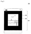
- Fig. 2 shows a state where the display area 104 is set up in the center of the area 102 which can be displayed of the display unit 100, and the image is displayed.
- the display area 104 is set up in the center of the area 102 which can be displayed to display the image
- the non-display area 106 is set around the display area 104, because the size of the image is smaller than the area 102 which can be displayed. It is favorable, considering a viewpoint of reduction of the power consumption and reduction of the degradation of the organic EL element constituting each pixel, that the luminance of the non-display area 106 is set zero, that is, blackout.
- the non-display area setting unit 36 displays the non-display area 106 in color of about from 30% to 35 % of white which is a guessed average luminance level of the general image to make the organic EL element in the non-display area 106 deteriorate to the same extent as the organic EL element in the display area 104.
- the degradation speed of the organic EL element in a whole screen can be averaged and the variation in the luminance and the phosphor burn-in phenomenon can be reduced.
- By reducing the variation in the luminance and phosphor burn-in it contributes also to an improvement of the life of the display unit 100.
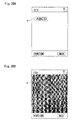
- Fig. 3 shows a state where an image having average luminance of a general image is set up to a non-display area.
- the image constituted by one color of about 30% of white is set up to the non-display area 106.
- the image which has arbitrary colors and patterns may be set as long as the average luminance thereof is about 30% of white.
- two or more images whose average luminance is about 30% of white should be prepared. The image should be replaced suitably and displayed to prevent the phosphor burn-in of the image.
- Fig. 4 shows a circuit structure of a single pixel of the display unit 100.
- This circuit comprises an organic light emitting element OLED, two transistors Tr1 and Tr2 for controlling the organic light emitting element OLED, a capacitor C, a scan line SL which transmits a scan signal, a data line DL which transmits a luminance data, and a power supply line Vdd which supplies current to the organic light emitting element.
- the power supply line Vdd supplies an electric current for making the organic light emitting element OLED emit.
- the data line DL transmits luminance data for controlling luminance of each of the organic light emitting elements OLED.
- the scanning line SL transmits scan signals for controlling the emitting timing of each of the organic light emitting elements OLED.
- the luminance data and the scan signal are supplied by the display control unit 38.
- a gate electrode of a first transistor Tr1 (hereinafter also referred to as “switching transistor") is connected to the scanning line SL.
- a drain electrode (or a source electrode) of the switching transistor Tr1 is connected to the data line DL.
- a source electrode (or a drain electrode) of the switching transistor Tr1 is connected to a gate electrode of a second transistor Tr2 (hereinafter also referred to as “driving transistor”).
- the switching transistor is a double-gate transistor having two gate electrodes.
- the switching transistor may be a single-gate transistor or a multi-gate transistor having three or more gate electrodes.
- the switching transistor Tr1 may be an n-channel transistor or a p-channel transistor.
- a source electrode (or a drain electrode) of the driving transistor Tr2 is connected to an anode of the organic light emitting element OLED.
- a drain electrode (or a source electrode) of the driving transistor Tr2 is connected to the power supply line Vdd. Similar to the switching transistor Tr1, the driving transistor Tr2 may be a single-gate transistor or a multi-gate transistor, and may be an n-channel transistor or a p-channel transistor.
- An anode of the organic light emitting element OLED is connected to the source electrode (or the drain electrode) of the driving transistor Tr2.
- a cathode of the organic light emitting element OLED is connected to ground potential.
- An electrode of the capacitor C is connected to the drain electrode (or the source electrode) of the switching transistor Tr1 and the gate electrode of the driving transistor Tr2.
- Another electrode of the capacitor C is connected to ground potential via a wire not shown in figures, or may be connected to the power supply line Vdd.
- the scan signal of the scanning line SL becomes high again, the switching transistor Tr1 turns on, then the new luminance data which is inputted to the data line DL is set in the driving transistor Tr2 and the capacitor C. Thereby, the organic light emitting element OLED emits corresponding to the new luminance data.
- the mobile terminal when the mobile terminal acquires the image to be displayed, the mobile terminal calculates average luminance of the image and selects an image to be displayed on the non-display area based on the average luminance.
- the internal structure of the mobile terminal according to this example is similar to the first example shown in Fig. 1. Hereinafter, a structure differing from that in the first embodiment will be mainly described.
- the non-display area setting unit 36 calculates the average luminance of the image acquired by the image acquiring unit 32.
- the average luminance may be calculated for every signal of R, G, and B.
- the non-display area setting unit 36 may calculate the average luminance of luminance signal Y.
- the non-display area setting unit 36 displays an image whose average luminance is substantially the same as the calculated average luminance.
- the image may be an image may be covered with the average luminosity value or an image with pattern which is prepared in the memory unit 40 beforehand. In the case of the patterned image, the phosphor burn-in of the image can be prevented by replacing two or more images suitably and displaying.
- an accumulated average luminance of images displayed on the display area and an accumulated average luminance of images displayed on the non-display area are stored, and the mobile terminal adjusts the images so that these accumulated average luminance values become almost the same for a long term.
- Fig. 5 shows an internal structure of the mobile terminal 10 according to the third example.
- the mobile terminal 10 of the present example further comprises an accumulated average luminance storing unit 44 in addition to the structure of the mobile terminal 10 of the first example shown in Fig. 1.
- a structure differing from that in the first embodiment will be mainly described.
- the non-display area setting unit 36 calculates the average luminance of the image.
- the non-display area setting unit 36 reads out the accumulated average luminance of the display area and the accumulated average luminance of the non-display area for the display area from the accumulated average luminance storing unit 44 according to the size of the image.
- the non-display area setting unit 36 selects an image to be displayed on the non-display area so that these accumulated average luminance values can approach. For example, when the accumulated average luminance of the display area is lower than the accumulated average luminance of the non-display area, the image whose average luminance is higher than the average luminance of the image to be displayed this time is set as the non-display area.
- the non-display area setting unit 36 recalculates the accumulated average luminance using the average luminance of the image displayed this time and the average luminance of the image displayed on the non-display area, and stores thus calculated accumulated average luminance in the accumulated average luminance storing unit 44.
- the accumulated average luminance may be calculated in consideration of display time.
- Fig. 6 shows an internal data of the accumulated average luminance storing unit 44.
- an area ID column 110 In the accumulated average luminance storing unit 44, an area ID column 110, a display area size column 112, a display area accumulated average luminance column 114, and a non-display area accumulated average luminance column 116.
- the size of the image acquired by the image acquiring unit 32 is 100 dots by 100 dots
- the information of the record of area ID "1" is read by the non-display area setting part 36.
- the non-display area setting unit 36 may adjust so that the accumulated average luminance of the display area and the non-display area may become equal by one display.
- the non-display area setting unit 36 may adjust so that the accumulated average luminance of the display area and the non-display area may become gradually equal by two or more displays.
- the flexibility of the image set as the non-display area spreads according to this method. For example, when displaying a photograph and the like, a frame may be displayed around the photograph. Surrounding image can be selected according to the kind or color of the image displayed or taste of a user.
- the image displayed on the non-display area may be fixed with the image set up first, and the accumulated average luminance of the display area and the non-display area may be calculated and stored when the display of the animation is completed. In the next display, the accumulated average luminance should just be adjusted so that they can approach.
- the variation in luminance of a display apparatus can be reduced and display quality can be improved according to this embodiment.
- the present embodiment relates to a mobile terminal comprising an organic EL (Electro Luminescence) display apparatus.
- organic EL Electro Luminescence
- an organic layer 213 is formed on a glass substrate 211 by arranging an organic hole transport layer 215 and an organic electron transport layer 216 on both sides of the organic luminescence layer 214.
- An organic EL panel is formed by arranging an anode 212 and a cathode 217 on both sides of the organic layer 213.
- the organic luminescence layer 214 emits light by applying a predetermined voltage between the anode 212 and the cathode 217.
- the anode 212 is made with transparent ITO (Indium Tin Oxide).
- the cathode 217 is made with Al-Li alloy for example. They are formed stripe type and arranged in the direction which crosses mutually configuring a matrix.
- the anode 212 is used for a data electrode
- the cathode 217 is used for a scanning electrode, for example.
- a voltage according to an input data is applied to each data electrode placed perpendicularly.
- the organic layer 213 emits light at the intersection of these electrodes and one line is displayed.
- the scanning electrode is scanned by switching perpendicularly one by one, and one field is displayed.
- An active matrix type driving mode is known as the driving mode of the organic EL display, in which luminescence of each pixel is continued over one vertical scanning term, other than the above-mentioned passive matrix type driving mode in which the time division driving is performed using the scanning electrode and the data electrode.
- each pixel 252 comprises an organic EL element 250 constituted by a part of the organic layer, a driving transistor TR2 which controls current supply to the organic EL element 250, a writing transistor TR1 which turns on by being applied a scanning voltage SCAN from the scanning electrode, and a capacitor element C which holds charge by being applied a data voltage DATA from the data electrode when the writing transistor TR1 turns on, as shown in Fig. 12.
- the output voltage of the capacitor C is applied to a gate of the driving transistor TR2.
- the operating state of the second transistor TR2 is determined by the charge quantity held in this capacitor C.
- the second transistor TR2 turns on, for example, current according to the data voltage is supplied to the organic EL element via the second transistor TR2. Consequently, The organic EL element 250 emits light with brightness according to the data voltage.
- the luminescence characteristic of the organic EL element deteriorates with progress of luminescence time, the luminance obtained by the same input current may decrease consequently.
- the luminescence frequency of pixels in a fixed area always becomes high when displaying a character of an e-mail on a screen. Thereby, the luminescence characteristic of these pixels deteriorate remarkably compared with other pixels. The problem so-called "phosphor burn-in" may arise as a result.
- the object of the present embodiment is to solve a problem of the "phosphor burn-in" with simple structure in a cellular phone comprising an organic EL display.
- the mobile terminal comprises an image processing circuit which can switch a display mode between a black character display mode in which a character part is displayed in black or a color with luminosity lower than that of a background part and the background part is displayed in white or a color with luminosity higher than that of the character part, and a white character display mode in which the background part is displayed in black or a color with luminosity lower than that of the character part and the character part is displayed in white or a color with luminosity higher than that of the background part, when displaying an electric mail on an organic electro-luminescence display apparatus; and a control circuit which controls an operation of said image processing circuit; wherein said control circuit alternately switches the display mode between the black character display mode and the white character display mode.
- the control circuit may instruct a mode switch between the black character display mode and the white character display mode in accordance with a predetermined rule in the concrete.
- a predetermined rule the rule of changing the mode between a display of transmitted mail and a display of received mail, and the rule of changing the mode with a fixed cycle are employable, for example.
- the control circuit may switch the mode at a random timing.
- the mode switching described above can be achieved by simple change of the control program.
- the black character display mode in which a character is displayed with lower luminance and the white character display mode in which a character is displayed with higher luminance can be switched with a predetermined cycle, at a predetermined timing according to an operation of a user, or at a random timing.
- the mobile telephone of the present embodiment comprises a transmission and reception circuit 202, an image processing circuit 203 for displaying an electronic mail received or to be transmitted by the transmission and reception circuit 202 on an organic EL display 201, a driving circuit 204 which drives the organic EL display 201 in response to an image signal from the image processing circuit 203, and a control circuit 205 consisted of a micro computer which controls operations of the transmission and reception circuit 202 and the image processing circuit 203.
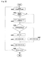
- Fig. 9 shows procedures performed in case the control circuit 205 displays an e-mail on the organic EL display 201. At first, it is judged whether an electronic mail to be displayed is transmitted mail or not, at the step S1.
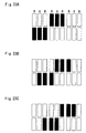
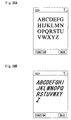
- a black character display mode in which a character part is displayed in black and a background part is displayed in white is set as shown in Fig. 8A, and the control circuit 205 supplies a mode switching signal to the image processing circuit 203, at the step S2.
- the control circuit 205 supplies a mode switching signal to the image processing circuit 203, at the step S3 of Fig. 9.
- the transmitted mail is displayed in the black character display mode on the organic EL display 201 as shown in Fig. 8A, and the received mail is displayed in the white character display mode on the organic EL display 201 as shown in Fig. 8B, consequently.
- Fig. 10 shows other procedures performed in case the control circuit 205 displays an e-mail on the organic EL display 201. At first, it is judged whether today is even-numbered day or not, at the step S11.
- a black character display mode in which a character part is displayed in black and a background part is displayed in white is set as shown in Fig. 8A, and the control circuit 205 supplies a mode switching signal to the image processing circuit 203, at the step S12.
- a white character display mode in which a character part is displayed in white and a background part is displayed in black is set, and the control circuit 205 supplies a mode switching signal to the image processing circuit 203, at the step S13 of Fig. 10.
- the transmitted mail and the received mail are displayed in the black character display mode on the organic EL display 201 at even-numbered day as shown in Fig. 8A, and displayed in the white character display mode on the organic EL display 201 at odd-numbered day as shown in Fig. 8B, consequently.
- the black character display mode and the white character display mode are switched by whether an E-mail is a transmitted mail or a received mail, or whether today is an even-numbered day or an odd-numbered day, the luminance of pixels which constitute the organic EL display 201 can be averaged in time over the whole screen, and deviation of the luminance can be reduced. Consequently, the "Phosphor burn-in" resulting from only some pixels carrying out age degradation early can be prevented.
- the power consumption of the organic EL display was large because the white background part occupies larger area than the black character part.
- the power consumption can be reduced because the black character display mode and the white character display mode can be switched.
- Various changing rules are employable, for example: a rule in which the black display mode and the white display mode are switched every time the power of the cellular phone is turned on; a rule in which the mode is switched every time a mail screen is displayed; a rule in which the mode is switched between a case of writing mail and a case of reading mail; a rule in which the mode is switched for every time or predetermined number of times on the occasion of a display of a mail at the time of mail creation; a rule in which the mode is switched for every time or predetermined number of times on the occasion of a display of a mail which has already been received or transmitted.
- the structure where the mode is switched at a random timing without following a predetermined rule can be adopted.
- the "phosphor burn-in" problem can be solved with simple component by a mobile terminal comprising an organic EL display according to the present embodiment.
- the present embodiment relates to a method for displaying a specific picture (a picture writing) called "PICT” like an antenna picture, a picture showing residual quantity of a battery, and the like, in a cellular phone comprising an organic EL (Electro Luminescence) display.
- PICT picture writing
- organic EL Electro Luminescence
- one color pixel is constituted by three kinds of organic EL elements (R luminescent element, G luminescent element, and B luminescent element) which emit R, G, and B light respectively.
- the luminescent elements deteriorates and luminance thereof decreases, if the color organic EL display is used over a long term. Especially, if large current is continuously supplied to the luminescent element, that is, the luminescent element continuously emits light with high luminance, the speed of reduction of luminance becomes high.
- the object of this embodiment is to provide a display method of a specific picture that can make hard to be conspicuous in luminance degradation with displaying the picture.
- a display method is a display method of a specific picture which is displayed on a color organic EL display and a lighting part thereof increases or decreases according to a situation, wherein the higher a probability of lighting of a part, the lower luminance of the part is set beforehand.
- a display method according to the second aspect of the present embodiment is a display method of the specific picture according to the first aspect, wherein the specific picture is a picture showing an antenna and/or a picture showing residual quantity of a battery.
- a display method is a display method of a specific picture which is displayed at areas which overlie each other on a color organic EL display, in which two or three kinds of the specific picture in roughly classification are switched and displayed according to a situation, wherein a dot which constitutes each specific picture is set up in a manner where a color of an emitting element turned on differs mutually among the two or three kinds of the specific picture.
- a display method is a display method of the specific picture according to the third aspect, wherein the specific picture is a picture of an antenna which is switched between a first picture showing an antenna bar and a second picture showing a character showing outside an area where an electric wave reaches.
- a display method is a display method of the specific picture according to the third aspect, wherein the specific picture is a picture showing residual quantity of a battery which is switched between a first picture showing a bar showing the residual quantity of the battery and a second picture showing a character showing a charge.
- a display method is a display method of a plurality of specific pictures which is displayed on a color organic EL display, wherein the higher a frequency of displaying a pixel is, the lower luminance of the pixel is set beforehand.
- Fig. 13 shows a schematic structure of a cellular phone.
- An MPU 3109 controls a cellular phone as a whole.
- An antenna 3101 transmits and receives an electric wave.
- a transmitter-receiver unit 3102 receives the electric wave and transmits the received content to the MPU 3109.
- the transmitter-receiver unit 3102 transmits a transmission signal outputted from the MPU 3109 with the electric wave.
- a microphone 3101 communicates an audio signal to the MPU 3109.
- a speaker 3104 outputs an audio signal outputted from the MPU 3109 as a sound.
- a first camera 3105 is a camera attached in the front of a main body of the cellular phone in which a color organic EL display 3114 is formed, and transmits shot image to the MPU 3109.
- a second camera 3106 is a camera attached in the back of the cellular phone, and transmits shot image to the MPU 3109. At a shooting mode, an image shot by the camera 3105 or 3106 is displayed on the color organic EL display 3114 instead of a display image at a normal mode.
- An operating unit 3108 is comprised in the main body of the cellular phone, includes various buttons and various switches.
- a flash memory 3110 data which should be saved when a power turns off are stored.
- a graphics memory 3112 image data to be displayed on the display is stored. Image data is written at the predetermined address in the graphics memory 3112 based on the image data and a write control signal outputted from the MPU 3109. Pixel data of the pixel corresponding with a display cycle of the color organic EL display is outputted from the graphics memory 3112 according to a scan timing.
- a timing control IC 3113 supplies a drive signal to the organic EL display 3114 with the image data, and displays an image on the color organic EL display 3114.
- a single color pixel is constituted with three kinds of organic EL elements (R luminescent element, G luminescent element, B luminescent element) which emit light in R, G, B, respectively.
- Such a color organic EL display 3114 includes the organic EL element for each color luminescence of RGB (R luminescent element, G luminescent element, B luminescent element).
- a battery residual quantity picture which shows residual quantity of a battery and an antenna picture which shows reception sensitivity are displayed on the upper part of the display screen of the color organic EL display 3114.
- the following three methods are proposed as the display method of such specific pictures.
- the first method is a display method of a specific picture which is displayed on a color organic EL display 314 and a lighting part thereof increases or decreases according to a situation, wherein the higher a probability of lighting of a part, the lower luminance of the part is set beforehand.
- the second method is a display method of a specific picture which is displayed at areas which overlie each other on a color organic EL display 3114, in which two or three kinds of the specific picture in roughly classification are switched and displayed according to a situation, wherein a dot which constitutes each specific picture is set up in a manner where a color of an emitting element turned on differs mutually among the two or three kinds of the specific picture.
- the third method is a display method of a plurality of specific pictures which is displayed on a color organic EL display 3114, wherein the higher a frequency of displaying a pixel is, the lower luminance of the pixel is set beforehand.
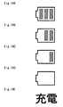
- a first picture showing a level of the residual quantity of the battery with 0 to 3 bars (Figs. 14A, 14B, 14C, 14D), and a second picture showing a character of "charge” (Fig. 14E) are prepared for displaying the battery residual quantity picture. This second picture is displayed when the residual quantity of the battery decreases extremely.
- the first picture consists of a battery frame figure imitated the battery and bars displayed in the battery frame figure. As shown in Figs. 14A, 14B, 14C, and 14D, the bars displayed in the battery frame figure change to four stages like 3, 2, 1, and 0. The more bars are displayed, the more residual quantity of the battery is left.
- Figs. 14A, 14B, 14C, 14D, and 14E Five kinds of images shown in Figs. 14A, 14B, 14C, 14D, and 14E are switched and displayed according to the battery residual quantity level.
- the first picture (bar) is displayed in green for example, and the second picture (character of "charge") is displayed in red.
- the higher a probability of lighting of a bar the lower the luminance of the bar is set beforehand.
- the probability of lighting of the rightmost bar is highest, the probability of lighting of the leftmost bar is lowest, and the probability of the middle bar is middle of the rightmost bar and the leftmost bar. Therefore, the display luminance of the rightmost bar 313 is set lowest, the display luminance of the leftmost bar 311 is set highest, and the display luminance of the middle bar 312 is set as the intermediate value thereof.
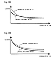
- Figs. 16A and 16B show a change over time of the display luminance of the rightmost bar which has high probability to light (solid line) and a change over time of the display luminance of the leftmost bar which has low probability to light (doted line).
- Fig. 16A shows a change over time of the display luminance in the case where the display luminance of the bar which has high probability to light is set low beforehand (the first method).
- Fig. 16B shows a change over time of the display luminance in the case where the display luminance of the bars are set as equal value beforehand (the conventional method).
- the reduction speed of the display luminance of the rightmost bar which has high probability of lighting is higher than that of the leftmost bar which has low probability of lighting. Thereby, the difference between the display luminance of these bars becomes gradually large when accumulated usage time of the cellular phone becomes long.
- the display luminance of the leftmost bar and the display luminance of the rightmost bar are gradually averaged and the difference between the display luminance of both becomes small as accumulative use time becomes large, because the display luminance of the bar which has higher probability of frequency of lighting is set lower beforehand. If it passes over the time when the difference between the display luminance of both becomes zero, the difference of the luminance spreads to the opposite direction. Use time can be extended until the difference of the luminance becomes incapable for visibility.
- the display luminance of each bars are gradually averaged and the differences between the display luminance values of each bars become small as accumulative use time becomes large, because the display luminance of the bar which has higher probability of frequency of lighting is set lower beforehand in the first method. If it passes over the time when the difference between the display luminance of each bars becomes zero, the difference of the luminance spreads to the opposite direction. Use time can be extended until the difference of the luminance becomes incapable for visibility.
- a first picture showing a receiving sensitivity with 0 to 3 bars (Figs. 17A, 17B, 17C, 17D), and a second picture showing a character of "outside" (Fig. 17E) are prepared for displaying the antenna picture. This second picture is displayed when the receiving sensitivity decreases extremely.
- the first picture consists of a antenna figure imitated the antenna and bars displayed right side of the antenna figure. As shown in Figs. 17A, 17B, 17C, and 17D, the bars displayed right side of the antenna figure change to four stages like 3, 2, 1, and 0. The more bars are displayed, the higher the receiving sensitivity of the antenna is.
- Figs. 17A-17E Five pictures shown in Figs. 17A-17E is switched and displayed according to receiving sensitivity.
- the first picture is displayed in green
- the second picture is displayed in red, for example.
- the higher a probability of lighting of a bar the lower the luminance of the bar is set beforehand.
- the probability of lighting of the leftmost bar is highest, the probability of lighting of the rightmost bar is lowest, and the probability of the middle bar is middle of the rightmost bar and the leftmost bar. Therefore, the display luminance of the leftmost bar 321 is set lowest, the display luminance of the rightmost bar 323 is set highest, and the display luminance of the middle bar 322 is set as the intermediate value thereof, as shown in Fig. 18.
- the display luminance of each bars are gradually averaged and the differences between the display luminance values of each bars become small as accumulative use time becomes large, because the display luminance of the bar which has higher probability of frequency of lighting is set lower beforehand in the first method. If it passes over the time when the difference between the display luminance of each bars becomes zero, the difference of the luminance spreads to the opposite direction. Use time can be extended until the difference of the luminance becomes incapable for visibility.
- a single color pixel is constituted with three kinds of organic EL elements (R luminescent element, G luminescent element, B luminescent element) which emit light in R, G, B, respectively. That is, the single color pixel is constituted with three dots.
- the first pictures showing residual quantity level of the battery with 0-3 bar(s) (Figs. 14A, 14B, 14C, 14D) and the second picture showing the character of "charge” (Fig. 14E) are switched and displayed according to the situation as mentioned above.
- the dots which constitute the first picture (bar) and the second picture (character of charge) are set in a manner where the kind of color of the emitting elements turned on when displaying these pictures differs each other.
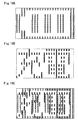
- Fig. 19A shows dots which constitute the picture (corresponding to the picture shown in Fig. 14A) in which the lighting pixels are most among the first pictures.
- Fig. 19B shows dots which constitute the second picture (corresponding to the picture shown in Fig. 14E).
- Fig. 19C shows a relation between the position of the dots which constitute the first picture and the position of the dots which constitute the second picture.
- the first picture is displayed only in green. All of the dots which constitute the first picture are G emitting elements.
- the second picture is displayed only in red. All of the dots which constitute the second picture are R emitting element.
- the dots which constitute either the first picture or the second picture may consist of the emitting elements of two colors (for example, R emitting element and G emitting element), and the dots which constitute another picture may consist of a color different from above-mentioned two colors (for example, B emitting element).
- the dots which constitute the first picture and the second picture are set in a manner where the kind of color of the emitting elements turned on when displaying these pictures differs each other.
- the one picture is not influenced by the degradation of the luminance of another picture among the first picture and the second picture, even if these pictures are displayed almost the same area.
- the second method can be also adopted to the first picture showing the receiving sensitivity with 0-3 bar(s) (Figs. 17A, 17B, 17C, 17D) and the second picture showing the character of "outside” (Fig. 17E) in the antenna picture.
- Fig. 20 shows pictures which can be displayed on upper part of the color organic EL display 3114.
- the higher a frequency of displaying the picture is, the lower luminance of the picture is set beforehand among these pictures 331-338.
- the picture 331 is a picture showing a state during a telephone call.
- the picture 331 is displayed only during the telephone call.
- the display luminance of thereof is set high beforehand because the frequency of a display of the picture 331 is low.
- the picture 332 is a picture showing residual quantity of the battery.
- the picture 332 is always displayed.
- the display luminance thereof is set low beforehand because the frequency of a display of the picture 332 is high.
- the picture 333 is a picture showing a state where a key of the cellular phone is locked.
- the picture 333 is only displayed when the key is locked.
- the display luminance thereof is set high beforehand because the frequency of a display of the picture 333 is low.
- the picture 334 is a picture showing a state where the cellular phone is in the manner mode.
- the picture 334 is only displayed when the cellular phone is in the manner mode.
- the display luminance thereof is set high beforehand because the frequency of a display of the picture 334 is low.
- the picture 335 is a picture showing a reception of a mail.
- the picture 334 is only displayed when the mail is received.
- the display luminance thereof is set high beforehand because the frequency of a display of the picture 335 is low.
- the picture 336 is a picture showing a state where a search on the web is performed.
- the picture 336 is only displayed when the search on the web is performed.
- the display luminance thereof is set high beforehand because the frequency of a display of the picture 336 is low.
- the picture 337 is a picture showing the antenna.
- the picture 337 is always displayed.
- the display luminance thereof is set low beforehand because the frequency of a display of the picture 337 is high.
- the picture 338 is a picture showing a state where the cellular phone is in the character input mode.
- the picture 338 is only displayed when the character is inputted.
- the display luminance thereof is set high beforehand because the frequency of a display of the picture 338 is low.
- the display luminance of the pictures 332 and 337 which are frequently displayed is set low among the pictures 331-338 in the example shown in Fig. 20.
- luminance degradation with displaying the specific picture can be made hard to be conspicuous.
- the present embodiment relates to a display apparatus and a display method, and it particularly relates to a technology for improving a display quality of the display apparatus and the display method.
- a liquid crystal display is mainly used as a display apparatus thereof.
- Organic EL (Electro Luminescence) display is expected as a next-generation flat display panel.
- the liquid crystal display the straitness of the view angle and the lateness of response speed still remain as a subject.
- the organic EL display can solve the above-mentioned subject and can achieve high luminosity and high efficiency.
- the organic EL display however, it can not be avoided a change with the passage of time, that is, degradation, of an optical element because of the characteristic thereof.
- a white balance may collapse or a variation of luminance may be arisen by continuous use, even if the white balance is adjusted at the time of manufacture.
- degradation of the optical element of the organic EL display is remarkable compared with that of the liquid crystal display, and it is recognized that it is a big problem in view of the quality of a product.
- the present embodiment has been made in view of the foregoing circumstances and an object thereof is to improve reduction of display quality caused by the above-mentioned variation of the luminance. Another object thereof is to avoid a phosphor burn-in of a display image caused by localizing the variation of the luminance.
- An aspect of the present embodiment relates to a display apparatus.
- This apparatus is a display apparatus comprising: an optical element; a luminance information storing unit which stores luminance information set to said optical element; and a display changing unit which changes a display image displayed on said display apparatus in a manner where a guessed value of degradation of each optical elements can be averaged based on the luminance information stored.
- the display apparatus means an apparatus comprising a display screen, for example, a cellular phone, a PDA (Personal Digital Assistant), a personal computer, and the like.
- An organic light emitting diode hereinafter, simply referred to as "OLED" as an optical element of an organic EL display deteriorates with passage of time as mentioned above. Cause of the deterioration is considered a current supplied to the OLED.
- the degradation of the OLED can be assumed by monitoring a luminance set to the OLED, for example, storing accumulated luminance set to the OLED, since the luminance of light emitted from the OLED is dependent on the current. If the degradation of the OLED is averaged, the variation of the luminance can be avoided.
- a specific character or a specific image is displayed on a specific position in the display screen of the cellular phone in many cases. It may cause the phosphor burn-in.
- the degradation of the OLED can be averaged by changing a display position, luminance, or color tone of the character and the image displayed.
- "average” may be a state almost equalized, and equalization should just be the grade where a user cannot recognize the variation of the luminance.
- the degradation speed of the OLEDs of R (Red), G (Green), and B (Blue) differs since the materials thereof differ each other. Thereby, there may be arisen a phenomenon that the display image is displayed in a little green for example as the display is used. Therefore, it is necessary to equalize the grade of degradation of the OLED of each color of R, G, and B.
- This apparatus is a display apparatus comprising: an optical element; and a display changing unit which changes a display image displayed on said display apparatus in a manner where a guessed value of degradation of each optical element can be averaged, maintaining an outline of the display image.
- This display apparatus is a display apparatus comprising: an optical element; a display screen which is composed of a plurality of display areas; and a display changing unit which changes a display image of each display area, maintaining an identity of a content of the display.
- a display screen of the cellular phone may be divided into a plurality of areas.
- a horizontally long and slender display area is set in the upper part of many cellular phones, and the picture which showing the residual quantity of a battery and the picture showing the intensity of an electric wave are displayed there. These pictures are always displayed. Thereby, if the display area of these pictures is burned in, there arises a possibility that a user can not recognize the residual quantity of the battery and the intensity of the electric wave. It is convenient that the picture displayed is changed for every divided area.
- the display changing unit may change the display image again, when a guessed value of degradation of the optical element reaches a predetermined value from the last change as a starting point.
- the display image may be changed when the accumulated value of the luminance set to the optical element exceeds a predetermined value, and the accumulated value of the luminance may be initialized in the case where the change is performed.
- the display changing unit may change the display image, when an absolute value of an accumulated difference of a luminance of neighboring pixels exceeds a predetermined value.
- the difference between the degradation of optical elements of neighboring pixels can be assumed by calculating the difference of the luminance thereof.
- the degradation of the pixel for a accumulating term can be assumed by accumulating the difference over the term.
- the display changing unit may change the display image, when a difference of a guessed value of degradation of the optical element in a row or a column of even number and odd number exceeds a predetermined value. That is, The display image may be changed when a difference between the accumulated luminance set to the even-numbered row and the accumulated luminance set to the odd-numbered row, or a difference between the accumulated luminance set to the even-numbered column and the accumulated luminance set to the odd-numbered column exceeds a predetermined value.
- the display image may be changed when following two conditions are fulfilled. First, the difference of the luminance set to the even-numbered and odd-numbered rows or columns in the image previously displayed is accumulated. The difference of the luminance set to the even-numbered and odd-numbered rows or columns in the image to be displayed next is accumulated. Then, the display image may be changed so that the degradation of the optical element can be averaged according to whether each accumulated value is positive or negative. Moreover, the luminance set to the even-numbered and odd-numbered rows or columns in the image previously displayed is accumulated. The luminance set to the even-numbered and odd-numbered rows or columns in the image to be displayed next is accumulated.
- the display image may be changed so that the degradation of the optical element can be averaged according to which of the accumulated values is greater.
- the display changing unit may change, when a power supply of the display apparatus is turned on or off, the display image in the process of turning the power on or off. For example, a user may not be noticed the change of the display image by changing the display image when the user does not see the display apparatus.
- the display changing unit may change, when an application displayed on the display apparatus is changed, the display image in the process of the change of the application.
- the display screen of the display apparatus can be opened and closed, the display apparatus may further comprise an opening-and-closing detecting unit which detects opening or closing of the display screen; and the display changing unit may change the display screen when opening and closing of the display screen are detected by the opening-and-closing detecting unit.
- An operating unit for operating the display apparatus may be slide-type; the display apparatus may further comprise a slide detecting unit which detects a slide of the operating unit; and the display changing unit may change the display screen when the slide of the operating unit is detected by the slide detecting unit.
- the display screen may be changed by operation of sliding out or closing of the operating unit.
- the display changing unit may change the display image by shifting a display position of the display image.
- the display changing unit may adjust a signal set up to each optical element according to a guessed value of degradation of the optical element.
- the degradation grade of the optical element may be assumed by accumulating the luminance set to the optical element as mentioned above.
- the luminance set to the optical element whose degradation is assumed large may be adjusted so that the variation of the luminance can be avoided based on the thus assumed value of degradation.
- the display changing unit may include an area detecting unit which detects a specific area, the display position thereof is to be shifted, among an area of the display image; and the display changing unit may change the display image by shifting the display position of the specific area detected.
- the display image can be relatively easily changed if the size and the display position is managed by an MPU or a memory comprised by the display apparatus.
- the display screen displayed on each may not be managed individually, but may be substantially managed as one display screen inside the display apparatus. Even in such a case, only a certain image displayed on the certain divided display screen may be shifted.
- a display screen of a cellular phone is exemplified.
- the display screen of the cellular phone comprises elongated display areas in top and bottom, and relatively large display area in middle.
- an image showing a state of an electric wave and an image showing residual quantity of a battery are displayed for example.
- an electric mail is displayed, or a background image is displayed when the cellular phone is not used.
- the display changing unit may determine an amount of compensation to be given to a signal according to a value of the signal, when adjusting the signal set up to said optical element. For example, if the same amount of compensation is given to the signal in the case where the low luminance is set to the optical element and in the case where the high luminance is set to the optical element, there is a possibility that the influence given to the display image in the case where the low luminance is set is larger. Thereby, a processing of reducing the amount of compensation given to the signal is performed when the low luminance is set.
- the display changing unit may determine an amount of compensation to be given to a signal based on the guessed value of degradation of the optical element of a surrounding pixel, when adjusting the signal set up to the optical element.
- the display changing unit may change the display image by changing a display color of each optical element.
- the display changing unit may change the display color for a predetermined cycle. As mentioned above, when the accumulated luminance is reached to a predetermined value, and there is not an input from a user for a predetermined term, in a case where the accumulated value of luminance of green is small for example, the whole display image may be changed to green.
- the change of the display color may be made by changing gradually a luminance ratio of the optical element corresponding to each color which constitutes a pixel.
- a display area needed for displaying an actual display image may be set up smaller than an effective display area which can be displayed in said display apparatus; and the display changing unit may shift the display area in the effective display area.
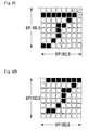
- the display area to be actually displayed may be 100*100 pixels, and five pixels of vertical and horizontal direction may be an area in which the image can be shifted.
- the optical element may correspond to a dot
- a pixel may include dots of a plurality of colors
- the display changing unit may shift the display image per dot, and may change combination of the optical elements which originally constitute one pixel.
- one pixel of the color display apparatus is generally constituted by dots of three colors of R, G, and B. Thereby, the display image may be shifted per pixel or per dot.
- the display changing unit may set a margin space which is originally set for displaying the character not to touch each other as an area in which the arbitrary character can be shifted.
- the font does not use one line in one side of the display area so that the font may not contact with a neighbor font, and the line is set as the margin area.
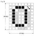
- the font In a case of the font of 16*16 pixels, for example, only 15*15 pixels are used actually. Thereby, each vertical and horizontal one line can be used as the display area of the font.
- the display changing unit may shift the display image to a direction in which influence for readability of the character is small when a user sees the character. For example, the display changing unit may scroll the character string horizontally when the user sees an e-mail on the display screen of the cellular phone.
- the display changing unit may scroll the display image or may perform a mosaic processing to the display image and displays it when there is no input from a user for predetermined period.
- a size of a block generated by the mosaic processing may be changed with passage of time.
- the display changing unit may select, when a background image which functions as a wallpaper is newly set up, the wallpaper according to grade of degradation of said optical element.
- set the wallpaper means both of a case where a new wallpaper is selected as the background image, and a case where a color of the displayed wallpaper is changed and set as the background image.
- the reduction of the luminance of each color can be averaged by changing the color of the wallpaper according to the grade of the assumed degradation of the optical element. Moreover, in a case where the reduction of the luminance of red is assumed large, the reduction of the luminance of each color can be averaged by setting an image in which green and blue is largely used as the wallpaper.
- the color tone of the wallpaper may be changed by adjusting the white balance of the selected wallpaper so that the degradation of the optical element corresponding to each color of RGB can be averaged. Since the advance degrees of degradation of the OLED of each color differ in the organic EL display especially, such a setup is highly effective.
- This method is a display method in a display apparatus which comprises an optical element, the method including: storing information of luminance set up to the optical element; and changing a display image displayed on the display apparatus in a manner where a guessed value of degradation of each optical element can be averaged based on the luminance information stored.
- This method is a display method in a display apparatus which comprises an optical element, the method including: changing a display image displayed on the display apparatus in a manner where a guessed value of degradation of each optical element can be averaged, maintaining an outline of the display image.
- Fig. 21 is a block diagram showing a basic structure of an organic EL display apparatus 410.
- the organic EL display apparatus 410 is constituted by an image source input unit 420, an organic EL driving circuit 430, and an organic EL panel 460.
- the organic EL driving circuit 430 comprises an image adjusting unit 432 which carries out various processings to a digital image signal inputted from the image source input unit 420, an MPU (Micro Processing Unit) 434 which calculates when these processings are carried out, and a DAC (Digital to Analog Converter) unit 442 which converts the image signal carried out processing to an analog signal.
- the organic EL driving circuit 430 further comprises a control signal generating unit which generates various timing control signals and a memory which functions a table when actual processing is carried out, which are not shown in the figure.
- the image adjusting unit 432 performs an offset adjusting to adjust a brightness, a gain adjusting to adjust a contrast, and a processing to adjust input image signal which is performed gamma correction to voltage-emitting luminance (V-T) characteristic of the organic EL panel.
- V-T voltage-emitting luminance
- the image adjusting unit 432 performs image adjusting processing like the offset adjusting and the gain adjusting.
- the digital signals are outputted from the DAC unit 442 as three kinds of analog signals R_out, G_out, and B_out to the organic EL panel 460.
- this structure can be realized by a CPU, a memory and other LSIs of an arbitrary computer.
- software it is realized by memory-loaded programs or the like, but drawn and described here are functional blocks that are realized in cooperation with those. Thus, it is understood by the skilled in the art that these functional blocks can be realized in a variety of forms by hardware only, software only or the combination thereof.
- luminance set to an OLED constituting each dot of a display screen is monitored.
- an accumulated value thereof reaches a predetermined condition, a part or the whole of a display image is shifted.
- the degradation of the OLED is averaged by averaging the luminance set to the OLED corresponding to each dot.
- a condition of the accumulated value for shifting the display image may be, for example, (1) when the accumulated value of the luminance in a predetermined term exceeds a predetermined value, (2) when the absolute value of the accumulated value of a difference between the luminance of neighboring pixels exceeds a predetermined value, (3) when a difference between the accumulated value of the luminance of an even-numbered column and that of an odd-numbered column exceeds a predetermined value.
- Fig. 22 shows a state where a character "0" is displayed on a display area of 9x8 pixels, and it is shifted one pixel to the right and down direction respectively.
- a character shown by black painting is a character before being shifted, and a character shown with slash is a character after being shifted.
- Figs. 23A, 23B, and 23C show an example in which a display image shifted per 1 dot.
- Fig. 23A shows an initial state before being shifted
- Fig. 23B shows a state where the display image is shifted one dot to right direction
- Fig. 23C shows a state where the display image is shifted 2dots to right direction.
- the initial state combination of colors of the dots which constitute a pixel is R, G, B in order from the left.
- the combination is G, B, R in order from the left.
- Fig. 24 shows a state where the display area A2 which is actually displayed is set up smaller than an effective display area A1 which can display the display picture.
- the effective display area A1 consists of 105x105 pixels.
- the display area A2 has an area in which the display image can be shifted 5 pixels in the length and the transverse direction each.
- Fig. 25 shows a state where a Japanese character is displayed on an area of 8x8 pixels. Pixels of the top line and the rightmost column are set up as a blank space area so that the character may not be touched with an adjoining character. This area is also used as a display area at the time of shifting a character.
- a character may shift 1 pixel to up, or 1 pixel to right, or not shift at all, for example. Thereby, phosphor burn-in can be reduced without spoiling display grace greatly.
- the above-mentioned shift of the display image may be carried out with a predetermined cycle.
- the shift can be performed without making a user conscious of the shift by shifting the display image when the user does not operate the display apparatus or the display screen is changed considerably.
- the timing of shifting may be, for example, (1) when the power of the display apparatus turns on or off, (2) when the display apparatus is opened or closed in a case where the display apparatus can be opened and closed like a fold-down type cellular phone, (3) when changing an application, (4) when there is no operation from a user for a predetermined term, (5) when an operating unit is slid out or closed in a case where the operating unit of the cellular phone is a slide type and can be opened and closed.
- Fig. 26 shows a structure of an organic EL display apparatus 4100 according to the present example.
- the basic structure is the same as the structure shown in Fig. 21 in the premise technology. Particularly characteristic structure in the present example will be explained.
- An organic EL driving circuit 430 includes a luminance accumulating unit 452 which acquires and stores luminance set to the OLED, a look-up table 343 which stores an above-mentioned condition about the accumulated luminance when shifting the display image and how to shift the display image, and a shift condition table 456 which stores above-mentioned timing of shifting.
- An image adjusting unit 432 includes an image shifting unit 450 which carries out processings for shifting and displaying the display image.
- the organic EL apparatus 4100 includes a mode switch detecting unit 470 which detects a timing of shifting the display image.
- the luminance accumulating unit 452 accumulates the luminance set to each OLED which constitutes each pixel and stores thus accumulated luminance.
- the image source input unit 420 includes an image changing unit 458 which carries out a mosaic processing and color change of the display image shown in examples 2-4 with reference to the accumulated luminance stored in the accumulated luminance storing unit 452.
- the mode detecting unit 470 detects the timing of shifting the display image, for example, when the application is changed and the like, and transmits the timing to the organic EL driving circuit 430.
- the MPU 434 refers to the shift condition table 456. If it is the timing to shift, the MPU 434 further refers to the look-up table 454 based on the accumulated luminance stored in the accumulated luminance storing unit 452. If the accumulated luminance is in the predetermined condition, the MPU 434 instructs to shift the display image to the image shifting unit 450.
- the degradation of specific OLED can be avoided and the phosphor burn-in of the display screen can be avoided by shifting the display image in accordance with the accumulated value of the luminance set to the OLED. Moreover, the degradation of the OLED in the whole display screen can be averaged and the variation of the luminance can be reduced.
- the display image is shifted per dot or per pixel under a predetermined condition.
- a predetermined time has passed after a user operation is completed, a part of the displayed image is scrolled horizontally or vertically, or is carried out a mosaic processing.
- Fig. 27A shows an initial display image, in which a white circle and a black triangle are displayed.
- Fig. 27B shows a state where images of the circle and the triangle are scrolled horizontally.
- Fig. 27C shows a state where images of the circle and the triangle are scrolled vertically.
- the degradation of the OLED is nearly equal in an area A3 where the image of the circle shown in Fig. 27B is scrolled.
- the average luminance in the whole display screen can be equaled by combination of the scroll to the horizontal direction and the scroll to the vertical direction.
- Figs. 28A and 28B show a state where the display image is carried out a mosaic processing. This processing is also carried out when a predetermined time has passed after completed the user operation.
- Fig. 28A shows a display image at an initial state.
- Fig. 28B shows a display image carried out the mosaic processing.
- the phosphor burn-in of the display screen can be further reduced by changing a size of a block generated by the mosaic processing with progress of time.
- the degradation of the OLED is averaged and the phosphor burn-in is reduced by shifting the display image.
- the degradation grade of the OLED emitting light of each color of R, G, and B is averaged by adjusting a signal set to the OLED corresponding to each dot and adjusting a color of the display image.
- the color may be adjusted only paying attention to a single pixel.
- the display image may be divided into blocks, 3*3 pixels for example, and the color may be adjusted so that balance in the block may be maintained.
- the blocks may be changed with progress of time.
- the amount of adjusting may be adjusted to make the color tone not change a lot.
- the adjusting may be made where the luminance ratio or R is made into 49%, and the luminance ratio of G and B are made into 51%, for example.
- Figs. 29A and 29B are schematic figures showing a state where a display color is changed at a fixed timing to average the emitting luminance of each color of RGB over time.
- the upper column shows an emitting color and the lower column shows amplitude of a signal. This change may be made per dot or may be performed to the whole display screen.
- Fig. 29A shows a state where only R is displayed among three colors of RGB.
- the amplitude of the signal set to the OLED is 0 except R.
- a predetermined time has passed after this state, only G is emitted as shown in Fig. 29B for example.
- RGB is emitted individually, but mixed colors may be emitted.
- the luminance ratio of RGB may be gradually changed as shown in Figs. 30A-30C.
- the signal amplitude of R becomes small and G emits light as shown in Fig. 30B.
- three colors of RGB emit light with the same signal amplitude as shown in Fig. 30C.
- Fig. 31 is a flowchart showing a procedure of a processing of the above-mentioned color change.
- the accumulated value is multiplied by a predetermined degradation rate and corrected (S418).
- the accumulated value of the luminance is inverted (S420).
- the signal for averaging the accumulated value in the display screen is outputted (S422). It subtracts from the inverted accumulated value according to the luminance set (S424) and the accumulated value of the luminance is updated (S426). If the updated accumulated value is averaged in the display screen (Y of S428), this color change processing is completed. If not averaged (N of S428), the steps S414 to S426 is repeated.
- the accumulated value is inverted and subtracted the set luminance, but the processing may not be restricted to this, the processing may be made as the maximum of the accumulated value is calculated, and the setup luminance is added to average the accumulated value.
- Fig. 32 is a flowchart showing a procedure of adjusting the display image according to the accumulated value of the luminance set to the OLED.
- the accumulated value of the luminance is acquired (S450).
- the accumulated value is multiplied by a predetermined degradation rate and corrected (S454).
- the accumulated value is updated reflecting the luminance set (S464). If the adjusting is continued (Y of S466), the steps S450 to S464 are repeated. If the adjusting is not continued (N of S466), the processing is ended.
- the gain is adjusted by multiplication of the signal, but the processing may not be restricted to this, the processing may be made by addition or subtraction of the signal.
- the processing may be made by addition or subtraction of the signal.
- color tone of the wallpaper is changed according to the grade of degradation of the OLED of each dot of a display screen.
- This change of the color tone may be made for vanishing the variation of the luminance caused by the degradation the OLED, or for averaging the grade of degradation of the OLED.
- the wallpaper is set up with the ratio of other G or the color of B being enlarged.
- the apparatus to realize this example can be realized with the structure shown in Fig. 26 of the first example.
- the same effect as the third example is acquired.
- Fig. 33 is a figure showing the display screen of the cellular phone.
- the display screen is divided into three areas of the first area L1, the second area L2, and the third area L3, in order from the top.
- a battery mark DM which is a picture showing residual quantity of the battery is displayed in left side
- an antenna mark AM which is a picture showing intensity of an electric wave is displayed in right side.
- the battery mark DM and the antenna mark AM are always displayed at a fixed position in many cellular phones. There is a probability of phosphor burn-in of these pictures. If the phosphor burn-in with a shape of the battery mark DM is arisen, there arises a probability that residual quantity of the battery cannot be shown properly to a user. Thereby, the battery mark DM and the antenna mark AM are shifted in only the first area L1.
- the horizontal scroll means shifting the battery mark DM and the antenna mark AM along a fixed direction.
- the horizontal swing means shifting the antenna mark DM and the antenna mark AM right and left by arbitrary number of pixels. That is, in the horizontal swing, the battery mark DM and the antenna mark AM is displayed swingingly.
- the visibility does not get worse so much by shifting the battery mark DM and the antenna mark AM only horizontally because the display position thereof can be roughly predicted.
- the picture displayed on the third area L3 is also shifted in the third area L3 maintaining visibility.
- the picture of a car displayed on the second area L2 (hereinafter simply referred to as a "car picture") TM may be scrolled arbitrary direction horizontally and vertically since the car picture is a background picture here, and the visibility thereof is not required from the user.
- the car picture TM displayed on the second area L2 in the middle once moves downward, then moves to down and right direction.
- Fig. 34 shows a state where the image displayed on the display screen shown in Fig. 33 is shifted.
- the battery mark DM and the antenna mark AM are scrolled right and left respectively. All the pictures displayed on the third area L3 are scrolled right.
- the car picture TM displayed on the second area L2 in middle is once shifted below, and shifted to right bottom after that.
- FIG. 35 is a figure showing the structure of the cellular phone 4200 according to the present example.
- the cellular phone 4200 comprises an MPU 434, a graphics memory 474, a timing control IC (Integrated Circuit) 476, a flash memory 472 and an organic EL panel 460.
- the cellular phone 4200 further comprises a speaker 462, a transmitter-receiver unit 464, and a microphone 466.
- the flash memory 472 stores data to be held when the power of the cellular phone 4200 is off.
- the graphics memory stores image data displayed on the organic EL panel 460.
- the image data is written in the graphics memory 474 when receiving the image data and a write position control of the image data from the MPU 434.
- the graphics memory 474 outputs the image in response to an input of a read control signal synchronized with the display from the timing control IC 476.
- the timing control IC 476 supplies the read control signal to the graphics memory 474 synchronizing with a scan timing of the organic EL panel 460 and reads the image data from the graphics memory 474.
- the timing control IC 476 supplies the thus read image data and a driving signal to the organic EL panel 460 and displays the display image on the organic EL panel 460.
- the timing control IC 476 also detects a vertically start point VS, a vertically end point VE, a horizontally start point HS, and a horizontally end point HE of the car picture TM displayed on the second area L2 shown in Fig. 33.
- Fig. 36 is a figure showing relation between the display image displayed on the organic EL panel 460 and not scrolled and the memory space.
- the display area of the organic EL panel 460 is constituted by 199*99 pixels.
- a left top position of this image corresponds to an address (0, 0) in the memory space and a right bottom position thereof corresponds to an address (199, 99).
- the image data is written at the address in which the display image corresponds one by one to the memory space in the graphics memory 474 by the MPU 434 as shown in Fig. 36.
- the scroll of the image in the organic EL panel 460 is performed by changing a timing of reading the image data by the timing control IC 476.
- the method of scrolling in the first area L1, the method of scrolling in the second area L2, and the method of scrolling in the third area L3 differ each other.
- the method of scrolling in the first area L1 and in the third area L3 may be the same.
- Reading the image data by the timing control IC 476 is explained based on Figs. 37A and 37B.
- Upper column shows the memory space and lower column shows the display image.
- Fig. 37A shows a procedure of reading the image data written in the memory space in the case without scroll.
- the image data written in the memory space is the same in Fig. 37A and in Fig. 37B.
- the read of the image data without scroll is carried out toward a horizontal direction one by one from the address (0, 0) S1 to the address (0, 99). Then, moving to the bottom of one line and the image data at the address (1, 0) is read. Similarly, the image data is sequentially read until the address (199, 99).
- the read of the image data with scroll is shown in Fig. 37B.
- the display image is scrolled only horizontally in the first area L1 and in the third area L3.
- the display image is shifted 50 pixels rightward.
- the display image is scrolled not only horizontally but vertically.
- the read of the image data is started at the address (0, 50).
- the image data is read sequentially.
- image data at the address (0, 99) moving back to the top of the line, image data from the address (0, 0) to the address (0, 49) is read.
- image data at the address (1, 50) in a lower row is read.
- the image data in the row is sequentially read.
- the car picture TM is displayed from the left top point GS.
- the image data is read from the address corresponding to the point GS. This address is referred to as the image start address M1 for convenience sake.
- the image data is read from the address M1. If the image data is read to the bottom row of the second area L2, the image data in the top row of the second area L2 is read. If the image data is read to the address just before the address M1, all of the image data in the second area L2 is read.
- the image data in the third area L3 is started. Similar to the display image in the first area L1, the display image in the third area L3 is shifted 50 pixels leftward. Therefore, read-out is started from the image data at the address moved horizontally 50. Read of the image data in the third area L3 is carried out like read of the image data in the first area L1.
- the MPU 434 is writing the image data in the graphics memory 474, the address of the start position GS of the image and the address of the end position GE of the image are grasped by the MPU 434. For this reason, the MPU 434 sets the read-out start address in the second area L2 so that the image may not be protruded from the organic EL panel 460.
- the scroll of the display image can be achieved by changing the address over time.
- the timing control IC 476 manages the size and the display position of the display image by detecting the image start position GS and the image end position GE of the display image.
- the MPU 434 writes the only required image data which is corrected from the last display image to the graphics memory 474 one after another. Thereby, the MPU 434 may be unable to manage the picture start position GS and the picture end position GE in the second area L2.
- the timing control IC 476 reads the image data from the memory
- the picture start position GS and the picture end position GE of the second area L2 can be detected.
- the MPU 434 can manage the display position of the image by notifying the detected picture start position GS and the picture end position GE to the MPU 434. Scrolling without a protrusion of the image can be realized by setting the read-out start address of the second area L2 to the timing control IC 476.
- the procedure of detecting the picture start position GS of the 2nd domain L2 by the timing control IC 476 and the picture end position GE is explained. It is assumed that a non-image area is covered with a single color as a premise.
- the address space of the second area L2 is known. If the data of the color which is not a non-image is outputted to the image data of the address in the second area L2, the timing control IC 476 detects the minimum address and the maximum address in horizontal and vertical for every frame.
- the detected addresses may be the picture start position GS and the picture end position GE in the second area L2.
- the non-image area means the area other than the car picture TM among the second area L2.
- generating of phosphor burn-in can be reduced by shifting independently the image displayed on the display screen of the cellular phone according to the divided area, without getting worse a user's visibility.
- the image shifting unit 450 which shifts a display image is comprised in the image adjusting unit 432, the image shifting unit 450 may be comprised in the image source input unit 420 and the display image inputted in the organic EL driving circuit may be changed.
- the above-mentioned three conditions of the accumulated value of luminance at the time of shifting the display image are exemplified, but not restricted with these.
- the difference of luminance set to the optical elements in the odd-numbered columns and the even-numbered columns may be accumulated until a certain time.
- the difference of luminance set to the OLEDs in the odd-numbered columns and the even-numbered columns in the image to be displayed next may be accumulated.
- the display image may be changed so that the degradation of the OLED may be averaged according to whether the accumulated value is positive or negative.
- the luminance set to the OLEDs in the odd-numbered columns and the even-numbered columns may be accumulated until a certain time.
- the luminance set to the OLEDs in the odd-numbered columns and the even-numbered columns in the image to be displayed next may be accumulated. Then, the display image may be changed so that the degradation of the OLED may be averaged according to which of the accumulated value is greater.
- the luminance set to the OLEDs in the even-numbered columns and the odd-numbered columns is compared, but the luminance set to the OLEDs in the even-numbered lines and the odd-numbered lines may be compared.
- the deterioration of display quality of the display apparatus can be suppressed according to the present embodiment. Particularly, the variation of the luminance in one screen and the deviation of the white balance can be mended. Moreover, the phosphor burn-in of a screen can be prevented in another viewpoint.
- the present embodiment relates to a display apparatus, and it particularly relates to a technology for improving a display quality of the display apparatus.
- a liquid crystal display is mainly used as a display apparatus thereof.
- Organic EL (Electro Luminescence) display is expected as a next-generation flat display panel.
- the liquid crystal display the straitness of the view angle and the lateness of response speed still remain as a subject.
- the organic EL display can solve the above-mentioned subject and can achieve high luminosity and high efficiency.
- the organic EL display however, it can not be avoided a change with the passage of time, that is, degradation, of an optical element because of the characteristic thereof.
- a white balance may collapse or a variation of luminance may be arisen by continuous use, even if the white balance is adjusted at the time of manufacture.
- degradation of the optical element of the organic EL display is remarkable compared with that of the liquid crystal display, and it is recognized that it is a big problem in view of the quality of a product.
- a specific character or a specific character string is continuously displayed on a specific place in many cases.
- both of a character and a character string are also referred to as a "character string.”
- a character string is set up so that it can be clearly distinguished from the color of the circumferences, such as a background picture. Therefore, a remarkable difference of advance of degradation between the optical elements of an area in which the character is displayed and the surrounding optical elements tends to appear.
- An object of the present embodiment is to improve reduction of display quality caused by the above-mentioned variation of the luminance. Another object of the present embodiment is to avoid a phosphor burn-in of a display image caused by localizing the variation of the luminance.
- An aspect of the present embodiment relates to a display apparatus.
- This display apparatus is a display apparatus comprising: an optical element; and a display changing unit which changes display form of a text data displayed on said display apparatus in a manner where a guessed value of degradation of each optical element can be averaged; wherein said display changing unit changes, when a power supply of said display apparatus is turned on or off, the display form of the text data in a process of turning the power on or off.
- the text data means a character.
- the display apparatus means an apparatus comprising a display screen, for example, a cellular phone, a PDA (Personal Digital Assistant), a personal computer, and the like.
- An organic light emitting diode hereinafter, simply referred to as "OLED" as an optical element of an organic EL display deteriorates with passage of time as mentioned above. Cause of the deterioration is considered a current supplied to the OLED.
- a specific character or a specific image is displayed on a specific position in the display screen of the cellular phone in many cases. It may cause the phosphor burn-in.
- the degradation of the OLED can be averaged by changing a display position, luminance, or color tone of the character and the image displayed.
- "average” may be a state almost equalized, and equalization should just be the grade where a user cannot recognize the variation of the luminance.
- the degradation speed of the OLEDs of R (Red), G (Green), and B (Blue) differs since the materials thereof differ each other. Thereby, there may be arisen a phenomenon that the display image is displayed in a little green for example as the display is used. Therefore, it is necessary to equalize the grade of degradation of the OLED of each color of R, G, and B.
- the change can be performed without making a user conscious by changing the display form of the text data when the user does not use the display apparatus.
- the form of the text data may be a kind, a size, a color, a brightness of the font for example. A color or a brightness of the background of the text data displayed may be changed.
- This display apparatus is a display apparatus comprising: an optical element; and a display changing unit which changes display form of a text data displayed on said display apparatus in a manner where a guessed value of degradation of each optical element can be averaged; wherein said display changing unit changes, when an application displayed on said display apparatus is changed, the display form of the text data in a process of the change of the application.
- the change of the application may be a change an application displayed on a display screen of a cellular phone from a web browser to an e-mail application for example.
- it is contained in the change of the application, in a case where the frame which displays a certain application is changed to another frame, even if the application is performed and displayed.
- the change of the frame which displays contents such as a homepage is included in the change of the application.
- E-mail software is displayed, for example, the change from the screen for selecting the E-mail received to the screen which displays the E-mail actually selected is included in the change of the application.
- This display apparatus is a display apparatus comprising: an optical element; and a display changing unit which changes display form of a text data displayed on said display apparatus in a manner where a guessed value of degradation of each optical element can be averaged; wherein said display changing unit changes, when an electric mail is displayed on said display apparatus, the display form of the text data for every electric mail. That is, the display form of the text data is changed according to the electric mail displayed when received electric mail is displayed or when the electric mail under creation or edit is displayed.
- This display apparatus is a display apparatus comprising an optical element, a display screen thereof can be opened and closed, the display apparatus comprising: a display changing unit which changes display form of a text data displayed on said display apparatus in a manner where a guessed value of degradation of each optical element can be averaged; and an opening-and-closing detecting unit which detects opening or closing of the display screen; wherein said display changing unit changes the display form of the text data when opening and closing of the display screen are detected by said opening-and-closing detecting unit.
- This display apparatus is a display apparatus comprising: an optical element; and a display changing unit which changes display form of a text data displayed on said display apparatus in a manner where a guessed value of degradation of each optical element can be averaged; wherein said display changing unit changes, while a character input means comprised in said display apparatus is operated for input of the character, the display form of the text data.
- the change of the display form of the text data is not limited to the change mentioned above, the color and the background color of the font may be reversed. The brightness of these colors may be adjusted according to the guessed value of the degradation of the optical element at the time of the reverse.
- This display apparatus is a display apparatus comprising: an optical element; and a display changing unit which changes display form of a text data displayed on said display apparatus in a manner where a guessed value of degradation of each optical element can be averaged; wherein said display changing unit changes, when an electric mail is displayed, the display form of the text data to be displayed according to whether the electric mail has already been read or has not been read yet. For example, a kind or size of a font of the electric mail which is already read or is not read yet when displaying the electric mail received.
- This display apparatus is a display apparatus comprising: an optical element; and a display changing unit which changes display form of a text data displayed on said display apparatus in a manner where a guessed value of degradation of each optical element can be averaged; wherein said display changing unit changes the display form of the text data according to the size of the text data to be displayed when an electric mail is displayed.
- the size of the font is set large in the case where the size of the text data is 10 characters, the size of the font is set small in the case where the size of the text data is 100 characters.
- the display changing unit may change the display form of the text data by changing a font type of the text data.
- the display changing unit may shift an arbitrary character included in the text data using a margin space which is originally set to avoid displaying the characters touching each other.
- the font does not use one line in one side of the display area so that the font may not contact with a neighbor font, and the line is set as the margin area.
- the line is set as the margin area.
- the font of 8*8 pixels for example, only 7*7 pixels are used actually. Thereby, each vertical and horizontal one line can be used as the display area of the font.
- This display apparatus is a display apparatus comprising: an optical element; and a display changing unit which changes display form of a text data displayed on said display apparatus in a manner where a guessed value of degradation of each optical element can be averaged; wherein said display changing unit sets a background color of a line in which the text data is not inputted as an intermediate color between a display color of the text data and an originally selected background color when an application for inputting the text data is executed.
- This display apparatus is a display apparatus comprising: an optical element; and a display changing unit which changes display form of a text data displayed on said display apparatus in a manner where a guessed value of degradation of each optical element can be averaged; wherein said display changing unit changes a luminance for displaying the text data according to a display position of the text data.
- a cellular phone comprising an organic EL display in a display screen as a display apparatus is considered.
- the phosphor burn-in of the organic EL display can be reduced by changing display form of a character string displayed on the cellular phone.
- the size or kind of the font of the character string to be displayed or the color thereof is changed when a user writes or reads an electric mail using the cellular phone.
- the font used for display is also changed when the power of the cellular phone is turned on or off.
- Figs. 38A and 38B show a display screen in which the phosphor burn-in is arisen.
- Fig. 38A four characters "ABCD" are displayed in an area A on the display screen. If these characters are displayed in the area A for a long term, the four characters "ABCD" are seen as if these characters are displayed there when an image in which all pixels are same color is displayed, even if these characters are not displayed. That is, the phosphor burn-in is arisen in the area A.
- the character string When a character string is displayed on the display screen of the cellular phone, the character string is generally displayed on the same part in many cases. Moreover, the character string is displayed from upper left of the display screen in many cases, and it is not often that the character string is displayed on lower part of the display screen. Then, the font type of the character displayed on the display screen is changed, or the luminance of the screen is changed according to the area of the display screen.
- the condition for changing the display form of the character string may be (1)when the power of the display apparatus is turned on or off, (2) when the display apparatus is opened or closed in a case where the display apparatus can be opened and closed like a fold-down type cellular phone, (3) when changing an application, (4) when a certain application, here, an e-mail application for example, is executed, (5) when there is no operation from a user for a predetermined term.
- the display form used may be changed according to whether the e-mail is already read or not, or the number of the characters included in the e-mail.
- Figs. 39A and 39B are figures showing a display screen in which a character string is displayed with two kinds of fonts different from each other.
- the font displayed in Fig. 39B is thin as a whole and inclines, compared with the font displayed in Fig. 39A.
- Fig. 39A five characters of the string are displayed on the fourth line, on the other hand, only one character of the string is displayed on the fourth line in Fig. 39B.
- An area where the character string is displayed may be changed by changing the font. That is, the phosphor burn-in of the display screen can be reduced by changing the kind of the font.
- Figs. 40A and 40B are figures showing a state where the size of the font used is changed when the number of the characters displayed on the display screen is different.
- fig. 40A 52 characters of alphabet from “A” to “Z” in a capital and small letter are displayed.
- Fig. 40B 26 characters of alphabet from “A” to “Z” in only capital letter are displayed.
- fig. 40B the number of the characters is decreased. If the font of the same size as the font displayed in Fig. 40A is used, the characters are displayed on only half of the display screen. Then, the character string can be displayed on the whole display screen by enlarging size of the font. Generally, when displaying a text and the like, the character string is displayed from the upper left of the display screen, and is not displayed on the bottom of the display screen in many cases. Then, text data can be displayed on the whole display screen by changing the size of the font.
- Fig. 41 is a figure showing a state where a color of an area where a character string is not displayed is gradually changed from a background color to a color same as the display color of the character string.
- the character string is displayed from the top to the fourth line.
- the character string is not displayed in the fifth to seventh lines.
- the color tone of these lines is gradually changed for every line so that the color may not be changed extremely. All the lines in which the character string is not displayed may be displayed in the same color, for example, an intermediate color between the color of the character and the color of the background.
- Figs. 42A and 42B are figures showing a state where a Japanese is displayed in an area of 8*8 pixels. The pixels of the top row and rightmost column of this area is set up as a margin space so that neighboring characters may not be touched. This area is also used as the display area at the time of shifting the character.
- Fig. 42A shows a state before the character is shifted
- Fig. 42B shows a state where the character string is shifted one pixel to up and right, respectively.
- a character may be shifted one pixel to up, another right, or further another not shifted, for example, depending on the character.
- the phosphor burn-in can be reduced without spoiling display quantity greatly.
- Fig. 43 is a block diagram showing a basic structure of an organic EL display apparatus 510.
- the organic EL display apparatus 510 is constituted by an image source input unit 520, an e-mail attribute acquiring unit 524, an open-close detecting unit 552, an operation detecting unit 554, an organic EL driving circuit 530, and an organic EL panel 560.
- the organic EL driving circuit 530 comprises an image adjusting unit 532 which carries out various processings to a digital image signal inputted from the image source input unit 520, an MPU (Micro Processing Unit) 534 which calculates when these processings are carried out, and a DAC (Digital to Analog Converter) unit 542 which converts the image signal carried out processing to an analog signal.
- the organic EL driving circuit 430 further comprises a text detecting unit 538, a luminance changing unit 544, and a color changing unit 546.
- the organic EL driving circuit 538 further comprises a control signal generating unit which generates various timing control signals and a memory which functions a table when actual processing is carried out, which are not shown in the figure.
- the image adjusting unit 532 performs an offset adjusting to adjust a brightness, a gain adjusting to adjust a contrast, and a processing to adjust input image signal which is performed gamma correction to voltage-emitting luminance (V-T) characteristic of the organic EL panel.
- V-T voltage-emitting luminance
- the image adjusting unit 532 When the display form of the character string is not changed, three kinds of the digital signals R_in, G_in, and B_in are inputted from the image source input unit 520 to the image adjusting unit 532.
- the image adjusting unit 532 performs image adjusting processing like the offset adjusting and the gain adjusting.
- the digital signals are outputted from the DAC unit 542 as three kinds of analog signals R_out, G_out, and B_out to the organic EL panel 560.
- the image adjusting unit 532 comprises a text shifting unit 536 which shifts the character to use an area where the character does not originally use among pixels which constitute the font as shown in Fig. 42.
- the text detecting unit 538 detects the character string from the inputted digital image signal.
- the text detecting unit 538 changes the display form of the detected character string in collaboration with the MPU 534 as shown in Figs. 39 and 40.
- the luminance changing unit 544 changes the luminance of the character according to a display position thereof.
- the luminance changing unit 544 also changes the luminance in an area where the character string is not inputted as shown in Fig. 41.
- the color changing unit 546 changes the color of the character and the color of an area where the character string is not inputted.
- the e-mail attribute acquiring unit 524 acquires an attribute of each e-mail when an e-mail application is executed.
- the attribute may be (1) whether the e-mail is already read or not, (2) the number of the characters included in the e-mail and the like.
- the image source input unit 520 further comprises a text form changing unit 522.
- the text form changing unit 522 changes the display form of the character string displayed in the e-mail based on the attribute acquired by the e-mail attribute acquiring unit 524.
- the change of the display form is also carried out by the text detecting unit 538, but the change here is carried out before the digital image signal is inputted to the organic EL driving circuit 524.
- the text detecting unit 538 may change the display form of the character string based on the attribute of the e-mail acquired by the e-mail attribute acquiring unit 524.
- the open-close detecting unit 552 detects open or close of the display screen in a case where the display screen of the cellular phone is a fold-down type.
- the open-close detecting unit 552 instructs the MPU 534 to change the display form of the character string used in the cellular phone when detecting.
- the operation detecting unit 554 instructs the MPU 534 to change the display form of the character string used in the cellular phone when there is no operation to the cellular phone for a predetermined term.
- this structure can be realized by a CPU, a memory and other LSIs of an arbitrary computer.
- software it is realized by memory-loaded programs or the like having a function of controlling display, but drawn and described here are functional blocks that are realized in cooperation with those.
- these functional blocks can be realized in a variety of forms by hardware only, software only or the combination thereof.
- the generation of the luminance variation in the display screen can be reduced by changing the display form of the character string and by changing the background color of the display screen according to whether the character string is displayed or not. Moreover, the phosphor burn-in of the display screen caused by the concentration of the luminance variation can be reduced.
- the present invention can be utilized for a display apparatus such as an organic EL display apparatus.
Landscapes
- Engineering & Computer Science (AREA)
- Physics & Mathematics (AREA)
- Computer Hardware Design (AREA)
- General Physics & Mathematics (AREA)
- Theoretical Computer Science (AREA)
- Signal Processing (AREA)
- Control Of Indicators Other Than Cathode Ray Tubes (AREA)
- Control Of El Displays (AREA)
- Electroluminescent Light Sources (AREA)
- Image Processing (AREA)
- Controls And Circuits For Display Device (AREA)
Abstract
A technology for reducing the so-called "phosphor
burn-in" phenomenon where the variation of luminance arises
by reducing display luminance of a certain pixel caused by
deterioration in a display apparatus constituted by an
organic electro-luminescence element is provided. In the
display apparatus (10), when displaying an image acquired by
an image acquiring unit (32), luminance substantially same
as average luminance of the acquired image is set to a non-display
area where the image is not displayed. Thereby,
degradation speed of the display elements in the whole
display screen can be averaged.
Description
The present invention relates to a display method
and a display apparatus, and it particularly relates to a
technology for averaging degradations of each optical
element in an active matrix type organic electro-luminescence
display apparatus and reducing variation of
luminance thereof.
Organic electro-luminescent displays (hereinafter,
also referred to as "organic EL displays" or "organic EL
panels") are attracting attention as new flat-type
displays. In particular, active matrix type organic EL
displays having thin film transistors (hereinafter, also
referred to as "TFTs") as switching elements are regarded
as sweeping out the currently prevailing liquid crystal
displays in the near future, and are in a fierce
development race for practical use.
Unlike liquid crystal displays, organic EL displays
have self-luminous elements. This eliminates the need
for a backlight which is indispensable to liquid crystal
displays, promising apparatuses of yet lower profile and
lighter weight. Moreover, organic EL panels are expected
for application as a light emitting devices such as the
backlight of liquid crystal displays using a self-luminous
characteristic.
It is known that, as for the organic EL element,
degradation progresses with luminescence and luminance
thereof gradually decreases. Development of the organic
luminescent material which does not deteriorate easily is
important for providing the organic EL panel with high
display quality and long life, of course, but it is
unescapable that degradation with the passage of time
arises for the organic EL element. The first thing to do
is development of the technology for suppressing the
influence of the degradation to the minimum at a present
stage.
The present invention has been made in view of the
foregoing circumstances and an object thereof is to
provide a technology for improving display quality of a
display apparatus.
An embodiment of the present invention relates to a
display method. In this display method, when displaying
an image on a display area narrower than an area which
can be displayed, luminance data of a non-displaying area
which does not display the image among the area which can
be displayed is set as a guessed value of an average
luminance of the image. "An area which can be displayed"
means a whole display screen in the display apparatus,
and "a display area" means an area where an image as an
object of display is actually displayed among the area
which can be displayed. "A non-displaying area" means an
area other than the display area among the area which can
be displayed. "Non-displaying" means that the image as
an object of display is not displayed, and does not
necessarily mean that nothing is displayed. The
degradation speed of the display element which
constitutes each pixel can be averaged over the whole
screen and the variation in the display luminance
resulting from the variation in degradation speed can be
reduced, by making the average luminance of the image
displayed on the display area and the average luminance
of the image displayed on the non-displaying area become
almost the same.
Another embodiment of the present invention relates
to a display apparatus. This display apparatus
comprising: an acquisition unit which acquires a first
image to be displayed; a first setting unit which sets a
first area in which the first image is displayed and
places the first image on the first area; and a second
setting unit which sets, when the first area is smaller
than an area which can be displayed, a second image to be
displayed on a second area in which the first image is
not displayed; wherein said second setting unit sets the
second image in a manner where a guessed value of an
average luminosity of the first image is substantially
same as a guessed value of an average luminosity of the
second image. The average luminance of a general image
may be guessed beforehand, and thus guessed average
luminance may be made become almost the same as the
average luminance of the second image. The luminance of
more than 30% and less than 40%, or more favorably more
than 30% and less than 35%, for example, of the maximum
luminance may be adapted as the average luminance of the
general picture.
The second setting unit may calculate the average
luminance of the first image and may set the second image
whose average luminance is substantially same as
calculated average luminance of the first image to the
second area. The degradation speed of the display
elements can be averaged with higher accuracy by
selecting the second image according to the average
luminance of the first image whenever the first image is
displayed.
Further another embodiment of the present invention
also relates to a display apparatus. This display
apparatus comprising: an acquisition unit which acquires
a first image to be displayed; a first setting unit which
sets a first area in which the first image is displayed
and places the first image on the first area; a second
setting unit which sets, when the first area is smaller
than an area which can be displayed, a second image to be
displayed on a second area in which the first image is
not displayed; a first storing unit which stores an
accumulative average luminance of the first image
previously displayed on the first area; and a second
storing unit which stores an accumulative average
luminance of the second image previously displayed on the
second area; wherein said second setting unit sets the
second image in a manner where the accumulative average
luminance of the second image approaches the accumulative
average luminance of the first image. Though the average
luminance of each first image differs from the average
luminance of each second image somewhat, it does not
necessarily lead to the variation in the display
luminance immediately. These average luminance should
just become almost the same for long term. The
accumulative average luminance of the first images and
second images may be stored, and the second image may be
adjusted to make these accumulative average luminance
values become almost the same for long term. The
variation in the display luminance can be reduced by this
method. According to this method, grater flexibility of
a display can be achieved. For example, the second image
can be selected based on the color or theme of the first
image.
The second image may be an image in which all
pixels have the almost same luminance data. That is, the
second image may be an image which consisted of only one
color. In this specification, the word an "image" is
used, even if the image consists of only one color.
Optional combinations of the aforementioned constituting
elements, and implementations of the invention in the
form of methods, apparatuses and systems may also be
practiced as additional modes of the present invention.
It is to be understood that any combinations of the
foregoing components, and expressions of the present
invention having their methods, apparatuses, systems,
recording media, computer programs, and the like
converted mutually are also intended to constitute
applicable aspects of the present invention.
The object described above, other objects,
characteristics and advantages will be appreciated by
referring to the preferred embodiments and associated
drawings.
In the present embodiment, in order to average
degradation speed of display elements which constitute
pixels of a display apparatus on the whole screen, and to
reduce variation in display luminosity resulting from
variation in degradation speed, when displaying an image, an
area where the image is not displayed is displayed in a
color of about 30% of white which is assumed as average
luminance of a general image.
Fig.1 shows an internal structure of a mobile terminal
10, as an example of a display apparatus of the present
embodiment. The mobile terminal 10 mainly comprises a
communication unit 20, a control unit 30, a memory unit 40,
a display unit 100, an input unit 50, a microphone 60, and a
speaker 70. The communication unit 20 includes an antenna
22 which transmits and receives a signal, a receiving unit
24 which decodes received signal, and a transmitting unit 26
which modulates and transmits data. The communication unit
20 controls communication with other apparatus via a
cellular phone network. The display unit 100 displays text
information, image information and the like. In this
embodiment, an organic EL panel is used as the display unit
100. The display unit 100 may be an inorganic EL panel or a
liquid crystal panel and the like. The technology of this
embodiment is especially suitable for the organic EL panel
with which degradation of the display element poses a
problem. The input unit 50 receives input information from
outside via a keyboard, mouse, button, and the like. The
microphone 60 inputs audio information from outside. The
speaker 70 outputs audio information to outside.
The control unit 30 controls of the mobile terminal 10
as a whole and performs various processings required for a
display. In terms of hardware, this structure can be
realized by a CPU, a memory and other LSIs of an arbitrary
computer. In terms of software, it is realized by memory-loaded
programs or the like having a function of controlling
display, but drawn and described here are functional blocks
that are realized in cooperation with those. Thus, it is
understood by the skilled in the art that these functional
blocks can be realized in a variety of forms by hardware
only, software only or the combination thereof.
The image acquiring unit 32 acquires an image to be
displayed from outside via the communication unit 20 or by
reading out the image stored in the memory unit 40. The
display area setting unit 34 sets an area to display the
image inside an area which can be displayed in the display
unit 100 according to the size of the acquired image. The
non-display area setting unit 36 sets an image to be
displayed on an area other than the display area among the
area which can be displayed, that is, a non-display area in
which the acquired image is not displayed. The display
control unit 38 places the image acquired by the image
acquiring unit 32 on the area set by the display area
setting unit 34, and sets the image set by the non-display
area setting unit 36 to the non-display area around the
display area. The display control unit 38 thus generates
the image data of the display screen and writes it to the
graphics memory 42. Then, the display control unit 38
outputs the image data and the driving signal to each pixel
of the display unit 100 at the predetermined timing.
Fig. 2 shows a state where the display area 104 is set
up in the center of the area 102 which can be displayed of
the display unit 100, and the image is displayed. In the
example shown in Fig. 2, the display area 104 is set up in
the center of the area 102 which can be displayed to display
the image, and the non-display area 106 is set around the
display area 104, because the size of the image is smaller
than the area 102 which can be displayed. It is favorable,
considering a viewpoint of reduction of the power
consumption and reduction of the degradation of the organic
EL element constituting each pixel, that the luminance of
the non-display area 106 is set zero, that is, blackout. If
an image is displayed on the display area 104 for a long
time, however, since the time in which the pixel of the
display area 104 is on becomes long as compared with the
pixel of the non-displaying area 106, degradation of the
organic EL element in the display area 104 will progress
earlier, and luminance will decrease. As a result thereof,
even if the whole screen is displayed with the same
luminance data, the luminance of the organic EL element near
center of the screen will become lower than the luminance of
the organic EL element near end of the screen, and a part
near center of the screen will be displayed darkly.
Especially, when displaying the image of the same size
frequently, as a result of continuing displaying an image on
the same display area 104 for a long time, the pixel in the
display area 104 deteriorates earlier than surrounding
pixels and the luminance thereof decreases. Consequently,
the so-called "phosphor burn-in" phenomenon will happen in
which the rectangle of the display area 104 is seen when
displaying an image on the whole screen.
In this embodiment, to reduce generating such a
phenomenon, the non-display area setting unit 36 displays
the non-display area 106 in color of about from 30% to 35 %
of white which is a guessed average luminance level of the
general image to make the organic EL element in the non-display
area 106 deteriorate to the same extent as the
organic EL element in the display area 104. Thereby, the
degradation speed of the organic EL element in a whole
screen can be averaged and the variation in the luminance
and the phosphor burn-in phenomenon can be reduced. By
reducing the variation in the luminance and phosphor burn-in,
it contributes also to an improvement of the life of the
display unit 100.
Fig. 3 shows a state where an image having average
luminance of a general image is set up to a non-display area.
In this example, the image constituted by one color of about
30% of white is set up to the non-display area 106. However,
the image which has arbitrary colors and patterns may be set
as long as the average luminance thereof is about 30% of
white. In the case where the patterned image is displayed
on the non-display area 106, two or more images whose
average luminance is about 30% of white should be prepared.
The image should be replaced suitably and displayed to
prevent the phosphor burn-in of the image.
Fig. 4 shows a circuit structure of a single pixel of
the display unit 100. This circuit comprises an organic
light emitting element OLED, two transistors Tr1 and Tr2 for
controlling the organic light emitting element OLED, a
capacitor C, a scan line SL which transmits a scan signal, a
data line DL which transmits a luminance data, and a power
supply line Vdd which supplies current to the organic light
emitting element.
The power supply line Vdd supplies an electric current
for making the organic light emitting element OLED emit.
The data line DL transmits luminance data for controlling
luminance of each of the organic light emitting elements
OLED. The scanning line SL transmits scan signals for
controlling the emitting timing of each of the organic light
emitting elements OLED. The luminance data and the scan
signal are supplied by the display control unit 38.
A gate electrode of a first transistor Tr1
(hereinafter also referred to as "switching transistor") is
connected to the scanning line SL. A drain electrode (or a
source electrode) of the switching transistor Tr1 is
connected to the data line DL. A source electrode (or a
drain electrode) of the switching transistor Tr1 is
connected to a gate electrode of a second transistor Tr2
(hereinafter also referred to as "driving transistor"). In
this embodiment, the switching transistor is a double-gate
transistor having two gate electrodes. In another
embodiment, the switching transistor may be a single-gate
transistor or a multi-gate transistor having three or more
gate electrodes. The switching transistor Tr1 may be an n-channel
transistor or a p-channel transistor.
A source electrode (or a drain electrode) of the
driving transistor Tr2 is connected to an anode of the
organic light emitting element OLED. A drain electrode (or
a source electrode) of the driving transistor Tr2 is
connected to the power supply line Vdd. Similar to the
switching transistor Tr1, the driving transistor Tr2 may be
a single-gate transistor or a multi-gate transistor, and may
be an n-channel transistor or a p-channel transistor.
An anode of the organic light emitting element OLED is
connected to the source electrode (or the drain electrode)
of the driving transistor Tr2. A cathode of the organic
light emitting element OLED is connected to ground potential.
An electrode of the capacitor C is connected to the drain
electrode (or the source electrode) of the switching
transistor Tr1 and the gate electrode of the driving
transistor Tr2. Another electrode of the capacitor C is
connected to ground potential via a wire not shown in
figures, or may be connected to the power supply line Vdd.
An operation of the circuit structured as described
above is explained hereinbelow. As the scan signal of the
scanning line SL goes high for writing the luminance data to
the organic light emitting element OLED, the switching
transistor Tr1 turns on, the luminance data which is being
inputted to the data line DL is set in the driving
transistor Tr2 and the capacitor C. A current which
corresponds to the luminance data thus flows between the
source electrode and the drain electrode of the driving
transistor Tr2, and this current flows in the organic light
emitting element OLED, so that the organic light emitting
element OLED emits. When the scan signal of the scanning
line SL becomes low, the switching transistor Tr1 turns off,
but the gate voltage of the driving transistor Tr2 is
maintained, so that the organic light emitting element OLED
continues emitting according to the set luminance data.
At the next emitting timing, the scan signal of the
scanning line SL becomes high again, the switching
transistor Tr1 turns on, then the new luminance data which
is inputted to the data line DL is set in the driving
transistor Tr2 and the capacitor C. Thereby, the organic
light emitting element OLED emits corresponding to the new
luminance data.
In this example, when the mobile terminal acquires the
image to be displayed, the mobile terminal calculates
average luminance of the image and selects an image to be
displayed on the non-display area based on the average
luminance. The internal structure of the mobile terminal
according to this example is similar to the first example
shown in Fig. 1. Hereinafter, a structure differing from
that in the first embodiment will be mainly described.
The non-display area setting unit 36 calculates the
average luminance of the image acquired by the image
acquiring unit 32. The average luminance may be calculated
for every signal of R, G, and B. The non-display area
setting unit 36 may calculate the average luminance of
luminance signal Y. The non-display area setting unit 36
displays an image whose average luminance is substantially
the same as the calculated average luminance. The image may
be an image may be covered with the average luminosity value
or an image with pattern which is prepared in the memory
unit 40 beforehand. In the case of the patterned image, the
phosphor burn-in of the image can be prevented by replacing
two or more images suitably and displaying.
In this example, an accumulated average luminance of
images displayed on the display area and an accumulated
average luminance of images displayed on the non-display
area are stored, and the mobile terminal adjusts the images
so that these accumulated average luminance values become
almost the same for a long term.
Fig. 5 shows an internal structure of the mobile
terminal 10 according to the third example. The mobile
terminal 10 of the present example further comprises an
accumulated average luminance storing unit 44 in addition to
the structure of the mobile terminal 10 of the first example
shown in Fig. 1. Hereinafter, a structure differing from
that in the first embodiment will be mainly described.
When the image acquiring unit 32 acquires an image to
be displayed, the non-display area setting unit 36
calculates the average luminance of the image. The non-display
area setting unit 36 reads out the accumulated
average luminance of the display area and the accumulated
average luminance of the non-display area for the display
area from the accumulated average luminance storing unit 44
according to the size of the image. The non-display area
setting unit 36 selects an image to be displayed on the non-display
area so that these accumulated average luminance
values can approach. For example, when the accumulated
average luminance of the display area is lower than the
accumulated average luminance of the non-display area, the
image whose average luminance is higher than the average
luminance of the image to be displayed this time is set as
the non-display area. Thereby, the average luminance of the
display area and the non-display area can be averaged in a
long term. The non-display area setting unit 36 recalculates
the accumulated average luminance using the
average luminance of the image displayed this time and the
average luminance of the image displayed on the non-display
area, and stores thus calculated accumulated average
luminance in the accumulated average luminance storing unit
44. When a display image is a still image, the accumulated
average luminance may be calculated in consideration of
display time.
Fig. 6 shows an internal data of the accumulated
average luminance storing unit 44. In the accumulated
average luminance storing unit 44, an area ID column 110, a
display area size column 112, a display area accumulated
average luminance column 114, and a non-display area
accumulated average luminance column 116. For example, when
the size of the image acquired by the image acquiring unit
32 is 100 dots by 100 dots, the information of the record of
area ID "1" is read by the non-display area setting part 36.
Since the accumulated average luminance of the display area
of area ID "1" is "70.5" and the accumulated average
luminance of the non-display area is "70.3", the average
luminance of the non-display area should just set up higher
than the average luminance of the display area in this time.
The non-display area setting unit 36 may adjust so that the
accumulated average luminance of the display area and the
non-display area may become equal by one display. The non-display
area setting unit 36 may adjust so that the
accumulated average luminance of the display area and the
non-display area may become gradually equal by two or more
displays.
The flexibility of the image set as the non-display
area spreads according to this method. For example, when
displaying a photograph and the like, a frame may be
displayed around the photograph. Surrounding image can be
selected according to the kind or color of the image
displayed or taste of a user. When displaying an animation
on the display area, if the average luminance of a
surrounding image is changed according to change of the
average luminance of the animation, there is a possibility
that the screen becomes hard to see. In this case, the
image displayed on the non-display area may be fixed with
the image set up first, and the accumulated average
luminance of the display area and the non-display area may
be calculated and stored when the display of the animation
is completed. In the next display, the accumulated average
luminance should just be adjusted so that they can approach.
Above-mentioned embodiments are only exemplary. It is
understood by those skilled in the art that there exist
other various modifications to the combination of each
component and process described above and that such
modifications are encompassed by the scope of the present
invention.
In this embodiment, explanation is made taking the
case of the mobile terminal as the display apparatus. The
technology of the present invention is not limited in this,
however, and can also be applied to the arbitrary display
apparatus like the television, the display of the computer.
The variation in luminance of a display apparatus can
be reduced and display quality can be improved according to
this embodiment.
The present embodiment relates to a mobile terminal
comprising an organic EL (Electro Luminescence) display
apparatus.
In recent years, development of an organic EL display
is progressing. For example, adopting the organic EL
display as a display of a cellular phone is in the air.
As shown in Fig. 11, an organic layer 213 is formed on
a glass substrate 211 by arranging an organic hole transport
layer 215 and an organic electron transport layer 216 on
both sides of the organic luminescence layer 214. An
organic EL panel is formed by arranging an anode 212 and a
cathode 217 on both sides of the organic layer 213. The
organic luminescence layer 214 emits light by applying a
predetermined voltage between the anode 212 and the cathode
217.
The anode 212 is made with transparent ITO (Indium Tin
Oxide). The cathode 217 is made with Al-Li alloy for
example. They are formed stripe type and arranged in the
direction which crosses mutually configuring a matrix.
The anode 212 is used for a data electrode, and the
cathode 217 is used for a scanning electrode, for example.
In the state where one scanning electrode placed
horizontally is selected, a voltage according to an input
data is applied to each data electrode placed
perpendicularly. Then the organic layer 213 emits light at
the intersection of these electrodes and one line is
displayed. The scanning electrode is scanned by switching
perpendicularly one by one, and one field is displayed.
An active matrix type driving mode is known as the
driving mode of the organic EL display, in which
luminescence of each pixel is continued over one vertical
scanning term, other than the above-mentioned passive matrix
type driving mode in which the time division driving is
performed using the scanning electrode and the data
electrode.
In the active matrix type organic EL display, each
pixel 252 comprises an organic EL element 250 constituted by
a part of the organic layer, a driving transistor TR2 which
controls current supply to the organic EL element 250, a
writing transistor TR1 which turns on by being applied a
scanning voltage SCAN from the scanning electrode, and a
capacitor element C which holds charge by being applied a
data voltage DATA from the data electrode when the writing
transistor TR1 turns on, as shown in Fig. 12. The output
voltage of the capacitor C is applied to a gate of the
driving transistor TR2.
At first, a voltage is applied to each scanning
electrode, then the first transistors Tr1 connected to this
scanning electrode turns on. The data voltage (input
signal) is applied to each data electrode synchronizing with
this scan. The data voltage is held in the capacitor C at
this time, because the first transistor TR1 is on.
The operating state of the second transistor TR2 is
determined by the charge quantity held in this capacitor C.
When the second transistor TR2 turns on, for example,
current according to the data voltage is supplied to the
organic EL element via the second transistor TR2.
Consequently, The organic EL element 250 emits light with
brightness according to the data voltage.
By the way, in the organic EL display, the
luminescence characteristic of the organic EL element
deteriorates with progress of luminescence time, the
luminance obtained by the same input current may decrease
consequently. In a cellular phone comprising the organic EL
display, the luminescence frequency of pixels in a fixed
area always becomes high when displaying a character of an
e-mail on a screen. Thereby, the luminescence
characteristic of these pixels deteriorate remarkably
compared with other pixels. The problem so-called "phosphor
burn-in" may arise as a result.
The object of the present embodiment is to solve a
problem of the "phosphor burn-in" with simple structure in a
cellular phone comprising an organic EL display.
The mobile terminal according to this embodiment
comprises an image processing circuit which can switch a
display mode between a black character display mode in which
a character part is displayed in black or a color with
luminosity lower than that of a background part and the
background part is displayed in white or a color with
luminosity higher than that of the character part, and a
white character display mode in which the background part is
displayed in black or a color with luminosity lower than
that of the character part and the character part is
displayed in white or a color with luminosity higher than
that of the background part, when displaying an electric
mail on an organic electro-luminescence display apparatus;
and a control circuit which controls an operation of said
image processing circuit; wherein said control circuit
alternately switches the display mode between the black
character display mode and the white character display mode.
The control circuit may instruct a mode switch between
the black character display mode and the white character
display mode in accordance with a predetermined rule in the
concrete. As a predetermined rule, the rule of changing the
mode between a display of transmitted mail and a display of
received mail, and the rule of changing the mode with a
fixed cycle are employable, for example.
The control circuit may switch the mode at a random
timing.
The mode switching described above can be achieved by
simple change of the control program.
In the mobile terminal according to the present
invention, the black character display mode in which a
character is displayed with lower luminance and the white
character display mode in which a character is displayed
with higher luminance can be switched with a predetermined
cycle, at a predetermined timing according to an operation
of a user, or at a random timing. Thereby, the situation
where only the pixel in a fixed area always emits light with
high luminance can be avoided, and the problem of "phosphor
burn-in" can be solved.
Hereinafter, an embodiment in which the present
invention is carried out to the cellular phone will be
concretely explained making reference to drawings.
As shown in Fig. 7, the mobile telephone of the
present embodiment comprises a transmission and reception
circuit 202, an image processing circuit 203 for displaying
an electronic mail received or to be transmitted by the
transmission and reception circuit 202 on an organic EL
display 201, a driving circuit 204 which drives the organic
EL display 201 in response to an image signal from the image
processing circuit 203, and a control circuit 205 consisted
of a micro computer which controls operations of the
transmission and reception circuit 202 and the image
processing circuit 203.
Fig. 9 shows procedures performed in case the control
circuit 205 displays an e-mail on the organic EL display 201.
At first, it is judged whether an electronic mail to be
displayed is transmitted mail or not, at the step S1.
If the mail to be displayed is a transmitted mail, a
black character display mode in which a character part is
displayed in black and a background part is displayed in
white is set as shown in Fig. 8A, and the control circuit
205 supplies a mode switching signal to the image processing
circuit 203, at the step S2.
On the other hand, if the mail to be displayed is a
received mail, a white character display mode in which a
character part is displayed in white and a background part
is displayed in black is set, and the control circuit 205
supplies a mode switching signal to the image processing
circuit 203, at the step S3 of Fig. 9.
The transmitted mail is displayed in the black
character display mode on the organic EL display 201 as
shown in Fig. 8A, and the received mail is displayed in the
white character display mode on the organic EL display 201
as shown in Fig. 8B, consequently.
Fig. 10 shows other procedures performed in case the
control circuit 205 displays an e-mail on the organic EL
display 201. At first, it is judged whether today is even-numbered
day or not, at the step S11.
If today is even-numbered day, a black character
display mode in which a character part is displayed in black
and a background part is displayed in white is set as shown
in Fig. 8A, and the control circuit 205 supplies a mode
switching signal to the image processing circuit 203, at the
step S12.
On the other hand, if today is odd-numbered day, a
white character display mode in which a character part is
displayed in white and a background part is displayed in
black is set, and the control circuit 205 supplies a mode
switching signal to the image processing circuit 203, at the
step S13 of Fig. 10.
The transmitted mail and the received mail are
displayed in the black character display mode on the organic
EL display 201 at even-numbered day as shown in Fig. 8A, and
displayed in the white character display mode on the organic
EL display 201 at odd-numbered day as shown in Fig. 8B,
consequently.
In the mobile telephone of the present embodiment,
since the black character display mode and the white
character display mode are switched by whether an E-mail is
a transmitted mail or a received mail, or whether today is
an even-numbered day or an odd-numbered day, the luminance
of pixels which constitute the organic EL display 201 can be
averaged in time over the whole screen, and deviation of the
luminance can be reduced. Consequently, the "Phosphor burn-in"
resulting from only some pixels carrying out age
degradation early can be prevented.
Moreover, in a conventional mobile telephone which
always displays a character part in black and a background
part in white, the power consumption of the organic EL
display was large because the white background part occupies
larger area than the black character part. In the mobile
telephone of the present embodiment, however, the power
consumption can be reduced because the black character
display mode and the white character display mode can be
switched.
Each component of the present invention is not limited
to the above-mentioned embodiment. Various changes can be
made without departing from the scope of the technology
which is described in the claims.
Various changing rules are employable, for example: a
rule in which the black display mode and the white display
mode are switched every time the power of the cellular phone
is turned on; a rule in which the mode is switched every
time a mail screen is displayed; a rule in which the mode is
switched between a case of writing mail and a case of
reading mail; a rule in which the mode is switched for every
time or predetermined number of times on the occasion of a
display of a mail at the time of mail creation; a rule in
which the mode is switched for every time or predetermined
number of times on the occasion of a display of a mail which
has already been received or transmitted. Moreover, the
structure where the mode is switched at a random timing
without following a predetermined rule can be adopted.
The "phosphor burn-in" problem can be solved with
simple component by a mobile terminal comprising an organic
EL display according to the present embodiment.
The present embodiment relates to a method for
displaying a specific picture (a picture writing) called
"PICT" like an antenna picture, a picture showing residual
quantity of a battery, and the like, in a cellular phone
comprising an organic EL (Electro Luminescence) display.
In a color organic EL display, one color pixel is
constituted by three kinds of organic EL elements (R
luminescent element, G luminescent element, and B
luminescent element) which emit R, G, and B light
respectively. The luminescent elements deteriorates and
luminance thereof decreases, if the color organic EL display
is used over a long term. Especially, if large current is
continuously supplied to the luminescent element, that is,
the luminescent element continuously emits light with high
luminance, the speed of reduction of luminance becomes high.
The object of this embodiment is to provide a display
method of a specific picture that can make hard to be
conspicuous in luminance degradation with displaying the
picture.
A display method according to the first aspect of the
present embodiment is a display method of a specific picture
which is displayed on a color organic EL display and a
lighting part thereof increases or decreases according to a
situation, wherein the higher a probability of lighting of a
part, the lower luminance of the part is set beforehand.
A display method according to the second aspect of the
present embodiment is a display method of the specific
picture according to the first aspect, wherein the specific
picture is a picture showing an antenna and/or a picture
showing residual quantity of a battery.
A display method according to the third aspect of the
present embodiment is a display method of a specific picture
which is displayed at areas which overlie each other on a
color organic EL display, in which two or three kinds of the
specific picture in roughly classification are switched and
displayed according to a situation, wherein a dot which
constitutes each specific picture is set up in a manner
where a color of an emitting element turned on differs
mutually among the two or three kinds of the specific
picture.
A display method according to the fourth aspect of the
present embodiment is a display method of the specific
picture according to the third aspect, wherein the specific
picture is a picture of an antenna which is switched between
a first picture showing an antenna bar and a second picture
showing a character showing outside an area where an
electric wave reaches.
A display method according to the fifth aspect of the
present embodiment is a display method of the specific
picture according to the third aspect, wherein the specific
picture is a picture showing residual quantity of a battery
which is switched between a first picture showing a bar
showing the residual quantity of the battery and a second
picture showing a character showing a charge.
A display method according to the sixth aspect of the
present embodiment is a display method of a plurality of
specific pictures which is displayed on a color organic EL
display, wherein the higher a frequency of displaying a
pixel is, the lower luminance of the pixel is set beforehand.
Hereinafter, an example where the present invention is
adopted to a cellular phone comprising a color organic EL
display will be explained with reference to drawings.
Fig. 13 shows a schematic structure of a cellular
phone. An MPU 3109 controls a cellular phone as a whole. An
antenna 3101 transmits and receives an electric wave. A
transmitter-receiver unit 3102 receives the electric wave
and transmits the received content to the MPU 3109. The
transmitter-receiver unit 3102 transmits a transmission
signal outputted from the MPU 3109 with the electric wave.
A microphone 3101 communicates an audio signal to the
MPU 3109. A speaker 3104 outputs an audio signal outputted
from the MPU 3109 as a sound. A first camera 3105 is a
camera attached in the front of a main body of the cellular
phone in which a color organic EL display 3114 is formed,
and transmits shot image to the MPU 3109. A second camera
3106 is a camera attached in the back of the cellular phone,
and transmits shot image to the MPU 3109. At a shooting
mode, an image shot by the camera 3105 or 3106 is displayed
on the color organic EL display 3114 instead of a display
image at a normal mode.
An operating unit 3108 is comprised in the main body
of the cellular phone, includes various buttons and various
switches. In a flash memory 3110, data which should be
saved when a power turns off are stored.
In a graphics memory 3112, image data to be displayed
on the display is stored. Image data is written at the
predetermined address in the graphics memory 3112 based on
the image data and a write control signal outputted from the
MPU 3109. Pixel data of the pixel corresponding with a
display cycle of the color organic EL display is outputted
from the graphics memory 3112 according to a scan timing.
A timing control IC 3113 supplies a drive signal to
the organic EL display 3114 with the image data, and
displays an image on the color organic EL display 3114.
In the color organic EL display 3114, a single color
pixel is constituted with three kinds of organic EL elements
(R luminescent element, G luminescent element, B luminescent
element) which emit light in R, G, B, respectively. Such a
color organic EL display 3114 includes the organic EL
element for each color luminescence of RGB (R luminescent
element, G luminescent element, B luminescent element).
In such a cellular phone, a battery residual quantity
picture which shows residual quantity of a battery and an
antenna picture which shows reception sensitivity are
displayed on the upper part of the display screen of the
color organic EL display 3114. In the present embodiment,
the following three methods are proposed as the display
method of such specific pictures.
The first method is a display method of a specific
picture which is displayed on a color organic EL display 314
and a lighting part thereof increases or decreases according
to a situation, wherein the higher a probability of lighting
of a part, the lower luminance of the part is set beforehand.
The second method is a display method of a specific
picture which is displayed at areas which overlie each other
on a color organic EL display 3114, in which two or three
kinds of the specific picture in roughly classification are
switched and displayed according to a situation, wherein a
dot which constitutes each specific picture is set up in a
manner where a color of an emitting element turned on
differs mutually among the two or three kinds of the
specific picture.
The third method is a display method of a plurality of
specific pictures which is displayed on a color organic EL
display 3114, wherein the higher a frequency of displaying a
pixel is, the lower luminance of the pixel is set beforehand.
Hereinafter, these method will be explained more
concretely.
As shown in Figs. 14A-14E, a first picture showing a
level of the residual quantity of the battery with 0 to 3
bars (Figs. 14A, 14B, 14C, 14D), and a second picture
showing a character of "charge" (Fig. 14E) are prepared for
displaying the battery residual quantity picture. This
second picture is displayed when the residual quantity of
the battery decreases extremely.
The first picture consists of a battery frame figure
imitated the battery and bars displayed in the battery frame
figure. As shown in Figs. 14A, 14B, 14C, and 14D, the bars
displayed in the battery frame figure change to four stages
like 3, 2, 1, and 0. The more bars are displayed, the more
residual quantity of the battery is left.
Five kinds of images shown in Figs. 14A, 14B, 14C, 14D,
and 14E are switched and displayed according to the battery
residual quantity level. The first picture (bar) is
displayed in green for example, and the second picture
(character of "charge") is displayed in red.
In the first method, the higher a probability of
lighting of a bar, the lower the luminance of the bar is set
beforehand. The probability of lighting of the rightmost
bar is highest, the probability of lighting of the leftmost
bar is lowest, and the probability of the middle bar is
middle of the rightmost bar and the leftmost bar. Therefore,
the display luminance of the rightmost bar 313 is set lowest,
the display luminance of the leftmost bar 311 is set highest,
and the display luminance of the middle bar 312 is set as
the intermediate value thereof.
Figs. 16A and 16B show a change over time of the
display luminance of the rightmost bar which has high
probability to light (solid line) and a change over time of
the display luminance of the leftmost bar which has low
probability to light (doted line).
Fig. 16A shows a change over time of the display
luminance in the case where the display luminance of the bar
which has high probability to light is set low beforehand
(the first method). Fig. 16B shows a change over time of
the display luminance in the case where the display
luminance of the bars are set as equal value beforehand (the
conventional method).
The reduction speed of the display luminance of the
rightmost bar which has high probability of lighting is
higher than that of the leftmost bar which has low
probability of lighting. Thereby, the difference between
the display luminance of these bars becomes gradually large
when accumulated usage time of the cellular phone becomes
long.
The display luminance of the leftmost bar and the
display luminance of the rightmost bar are gradually
averaged and the difference between the display luminance of
both becomes small as accumulative use time becomes large,
because the display luminance of the bar which has higher
probability of frequency of lighting is set lower beforehand.
If it passes over the time when the difference between the
display luminance of both becomes zero, the difference of
the luminance spreads to the opposite direction. Use time
can be extended until the difference of the luminance
becomes incapable for visibility.
Considering three bars, the display luminance of each
bars are gradually averaged and the differences between the
display luminance values of each bars become small as
accumulative use time becomes large, because the display
luminance of the bar which has higher probability of
frequency of lighting is set lower beforehand in the first
method. If it passes over the time when the difference
between the display luminance of each bars becomes zero, the
difference of the luminance spreads to the opposite
direction. Use time can be extended until the difference of
the luminance becomes incapable for visibility.
As shown in Figs. 17A-17E, a first picture showing a
receiving sensitivity with 0 to 3 bars (Figs. 17A, 17B, 17C,
17D), and a second picture showing a character of "outside"
(Fig. 17E) are prepared for displaying the antenna picture.
This second picture is displayed when the receiving
sensitivity decreases extremely.
The first picture consists of a antenna figure
imitated the antenna and bars displayed right side of the
antenna figure. As shown in Figs. 17A, 17B, 17C, and 17D,
the bars displayed right side of the antenna figure change
to four stages like 3, 2, 1, and 0. The more bars are
displayed, the higher the receiving sensitivity of the
antenna is.
Five pictures shown in Figs. 17A-17E is switched and
displayed according to receiving sensitivity. The first
picture is displayed in green, the second picture is
displayed in red, for example.
In the first method, the higher a probability of
lighting of a bar, the lower the luminance of the bar is set
beforehand. The probability of lighting of the leftmost bar
is highest, the probability of lighting of the rightmost bar
is lowest, and the probability of the middle bar is middle
of the rightmost bar and the leftmost bar. Therefore, the
display luminance of the leftmost bar 321 is set lowest, the
display luminance of the rightmost bar 323 is set highest,
and the display luminance of the middle bar 322 is set as
the intermediate value thereof, as shown in Fig. 18.
Also in this case, the display luminance of each bars
are gradually averaged and the differences between the
display luminance values of each bars become small as
accumulative use time becomes large, because the display
luminance of the bar which has higher probability of
frequency of lighting is set lower beforehand in the first
method. If it passes over the time when the difference
between the display luminance of each bars becomes zero, the
difference of the luminance spreads to the opposite
direction. Use time can be extended until the difference of
the luminance becomes incapable for visibility.
A display method of a specific picture which is
displayed at areas which overlie each other on a color
organic EL display, in which two or three kinds of the
specific picture in roughly classification are switched and
displayed according to a situation, wherein a dot which
constitutes each specific picture is set up in a manner
where a color of an emitting element turned on differs
mutually among the two or three kinds of the specific
picture.
As mentioned above, in the color organic EL display
3114, a single color pixel is constituted with three kinds
of organic EL elements (R luminescent element, G luminescent
element, B luminescent element) which emit light in R, G, B,
respectively. That is, the single color pixel is
constituted with three dots.
As the battery residual quantity picture, the first
pictures showing residual quantity level of the battery with
0-3 bar(s) (Figs. 14A, 14B, 14C, 14D) and the second picture
showing the character of "charge" (Fig. 14E) are switched
and displayed according to the situation as mentioned above.
In the second method, the dots which constitute the
first picture (bar) and the second picture (character of
charge) are set in a manner where the kind of color of the
emitting elements turned on when displaying these pictures
differs each other.
Fig. 19A shows dots which constitute the picture
(corresponding to the picture shown in Fig. 14A) in which
the lighting pixels are most among the first pictures. Fig.
19B shows dots which constitute the second picture
(corresponding to the picture shown in Fig. 14E). Fig. 19C
shows a relation between the position of the dots which
constitute the first picture and the position of the dots
which constitute the second picture.
In this example, the first picture is displayed only
in green. All of the dots which constitute the first
picture are G emitting elements. On the other hand, the
second picture is displayed only in red. All of the dots
which constitute the second picture are R emitting element.
The dots which constitute either the first picture or
the second picture may consist of the emitting elements of
two colors (for example, R emitting element and G emitting
element), and the dots which constitute another picture may
consist of a color different from above-mentioned two colors
(for example, B emitting element).
In the second method, the dots which constitute the
first picture and the second picture are set in a manner
where the kind of color of the emitting elements turned on
when displaying these pictures differs each other.
Therefore, the one picture is not influenced by the
degradation of the luminance of another picture among the
first picture and the second picture, even if these pictures
are displayed almost the same area.
The second method can be also adopted to the first
picture showing the receiving sensitivity with 0-3 bar(s)
(Figs. 17A, 17B, 17C, 17D) and the second picture showing
the character of "outside" (Fig. 17E) in the antenna picture.
Fig. 20 shows pictures which can be displayed on upper
part of the color organic EL display 3114.
In the third method, the higher a frequency of
displaying the picture is, the lower luminance of the
picture is set beforehand among these pictures 331-338.
Concretely, the picture 331 is a picture showing a
state during a telephone call. The picture 331 is displayed
only during the telephone call. The display luminance of
thereof is set high beforehand because the frequency of a
display of the picture 331 is low.
The picture 332 is a picture showing residual quantity
of the battery. The picture 332 is always displayed. The
display luminance thereof is set low beforehand because the
frequency of a display of the picture 332 is high.
The picture 333 is a picture showing a state where a
key of the cellular phone is locked. The picture 333 is
only displayed when the key is locked. The display
luminance thereof is set high beforehand because the
frequency of a display of the picture 333 is low.
The picture 334 is a picture showing a state where the
cellular phone is in the manner mode. The picture 334 is
only displayed when the cellular phone is in the manner mode.
The display luminance thereof is set high beforehand because
the frequency of a display of the picture 334 is low.
The picture 335 is a picture showing a reception of a
mail. The picture 334 is only displayed when the mail is
received. The display luminance thereof is set high
beforehand because the frequency of a display of the picture
335 is low.
The picture 336 is a picture showing a state where a
search on the web is performed. The picture 336 is only
displayed when the search on the web is performed. The
display luminance thereof is set high beforehand because the
frequency of a display of the picture 336 is low.
The picture 337 is a picture showing the antenna. The
picture 337 is always displayed. The display luminance
thereof is set low beforehand because the frequency of a
display of the picture 337 is high.
The picture 338 is a picture showing a state where the
cellular phone is in the character input mode. The picture
338 is only displayed when the character is inputted. The
display luminance thereof is set high beforehand because the
frequency of a display of the picture 338 is low.
That is, the display luminance of the pictures 332 and
337 which are frequently displayed is set low among the
pictures 331-338 in the example shown in Fig. 20.
According to the present embodiment, luminance
degradation with displaying the specific picture can be made
hard to be conspicuous.
The present embodiment relates to a display apparatus
and a display method, and it particularly relates to a
technology for improving a display quality of the display
apparatus and the display method.
Notebook type personal computers and mobile terminals
are spreading widely. A liquid crystal display is mainly
used as a display apparatus thereof. Organic EL (Electro
Luminescence) display is expected as a next-generation flat
display panel. As for the liquid crystal display, the
straitness of the view angle and the lateness of response
speed still remain as a subject. On the other hand, the
organic EL display can solve the above-mentioned subject and
can achieve high luminosity and high efficiency.
As for the organic EL display, however, it can not be
avoided a change with the passage of time, that is,
degradation, of an optical element because of the
characteristic thereof. A white balance may collapse or a
variation of luminance may be arisen by continuous use, even
if the white balance is adjusted at the time of manufacture.
It is known that degradation of the optical element of the
organic EL display is remarkable compared with that of the
liquid crystal display, and it is recognized that it is a
big problem in view of the quality of a product.
The present embodiment has been made in view of the
foregoing circumstances and an object thereof is to improve
reduction of display quality caused by the above-mentioned
variation of the luminance. Another object thereof is to
avoid a phosphor burn-in of a display image caused by
localizing the variation of the luminance.
An aspect of the present embodiment relates to a
display apparatus. This apparatus is a display apparatus
comprising: an optical element; a luminance information
storing unit which stores luminance information set to said
optical element; and a display changing unit which changes a
display image displayed on said display apparatus in a
manner where a guessed value of degradation of each optical
elements can be averaged based on the luminance information
stored.
Here, the display apparatus means an apparatus
comprising a display screen, for example, a cellular phone,
a PDA (Personal Digital Assistant), a personal computer, and
the like. An organic light emitting diode (hereinafter,
simply referred to as "OLED") as an optical element of an
organic EL display deteriorates with passage of time as
mentioned above. Cause of the deterioration is considered a
current supplied to the OLED. The degradation of the OLED
can be assumed by monitoring a luminance set to the OLED,
for example, storing accumulated luminance set to the OLED,
since the luminance of light emitted from the OLED is
dependent on the current. If the degradation of the OLED is
averaged, the variation of the luminance can be avoided.
Generally, a specific character or a specific image is
displayed on a specific position in the display screen of
the cellular phone in many cases. It may cause the phosphor
burn-in. The degradation of the OLED can be averaged by
changing a display position, luminance, or color tone of the
character and the image displayed. Here, "average" may be a
state almost equalized, and equalization should just be the
grade where a user cannot recognize the variation of the
luminance.
In the case of color display in the organic EL display,
the degradation speed of the OLEDs of R (Red), G (Green),
and B (Blue) differs since the materials thereof differ each
other. Thereby, there may be arisen a phenomenon that the
display image is displayed in a little green for example as
the display is used. Therefore, it is necessary to equalize
the grade of degradation of the OLED of each color of R, G,
and B.
Another aspect of the present embodiment also relates
to a display apparatus. This apparatus is a display
apparatus comprising: an optical element; and a display
changing unit which changes a display image displayed on
said display apparatus in a manner where a guessed value of
degradation of each optical element can be averaged,
maintaining an outline of the display image.
Further another aspect of the present embodiment also
relates to a display apparatus. This display apparatus is a
display apparatus comprising: an optical element; a display
screen which is composed of a plurality of display areas;
and a display changing unit which changes a display image of
each display area, maintaining an identity of a content of
the display.
A display screen of the cellular phone, for example,
may be divided into a plurality of areas. A horizontally
long and slender display area is set in the upper part of
many cellular phones, and the picture which showing the
residual quantity of a battery and the picture showing the
intensity of an electric wave are displayed there. These
pictures are always displayed. Thereby, if the display area
of these pictures is burned in, there arises a possibility
that a user can not recognize the residual quantity of the
battery and the intensity of the electric wave. It is
convenient that the picture displayed is changed for every
divided area.
The display changing unit may change the display image
again, when a guessed value of degradation of the optical
element reaches a predetermined value from the last change
as a starting point. For example, the display image may be
changed when the accumulated value of the luminance set to
the optical element exceeds a predetermined value, and the
accumulated value of the luminance may be initialized in the
case where the change is performed. The display changing
unit may change the display image, when an absolute value of
an accumulated difference of a luminance of neighboring
pixels exceeds a predetermined value.
That is, the difference between the degradation of
optical elements of neighboring pixels can be assumed by
calculating the difference of the luminance thereof. The
degradation of the pixel for a accumulating term can be
assumed by accumulating the difference over the term.
The display changing unit may change the display image,
when a difference of a guessed value of degradation of the
optical element in a row or a column of even number and odd
number exceeds a predetermined value. That is, The display
image may be changed when a difference between the
accumulated luminance set to the even-numbered row and the
accumulated luminance set to the odd-numbered row, or a
difference between the accumulated luminance set to the
even-numbered column and the accumulated luminance set to
the odd-numbered column exceeds a predetermined value.
The display image may be changed when following two
conditions are fulfilled. First, the difference of the
luminance set to the even-numbered and odd-numbered rows or
columns in the image previously displayed is accumulated.
The difference of the luminance set to the even-numbered and
odd-numbered rows or columns in the image to be displayed
next is accumulated. Then, the display image may be changed
so that the degradation of the optical element can be
averaged according to whether each accumulated value is
positive or negative. Moreover, the luminance set to the
even-numbered and odd-numbered rows or columns in the image
previously displayed is accumulated. The luminance set to
the even-numbered and odd-numbered rows or columns in the
image to be displayed next is accumulated. Then, the
display image may be changed so that the degradation of the
optical element can be averaged according to which of the
accumulated values is greater. In the case of these two
conditions, it is not necessary to prepare a memory storing
a predetermined value which is a threshold value at the time
of changing the display image in a circuit.
The display changing unit may change, when a power
supply of the display apparatus is turned on or off, the
display image in the process of turning the power on or off.
For example, a user may not be noticed the change of the
display image by changing the display image when the user
does not see the display apparatus. The display changing
unit may change, when an application displayed on the
display apparatus is changed, the display image in the
process of the change of the application.
The display screen of the display apparatus can be
opened and closed, the display apparatus may further
comprise an opening-and-closing detecting unit which detects
opening or closing of the display screen; and the display
changing unit may change the display screen when opening and
closing of the display screen are detected by the opening-and-closing
detecting unit. An operating unit for operating
the display apparatus may be slide-type; the display
apparatus may further comprise a slide detecting unit which
detects a slide of the operating unit; and the display
changing unit may change the display screen when the slide
of the operating unit is detected by the slide detecting
unit. For example, in the case where the operating unit
like a keyboard is normally hidden under the display screen
and is slid out when operating in the cellular phone, the
display screen may be changed by operation of sliding out or
closing of the operating unit.
The display changing unit may change the display image
by shifting a display position of the display image. The
display changing unit may adjust a signal set up to each
optical element according to a guessed value of degradation
of the optical element. For example, the degradation grade
of the optical element may be assumed by accumulating the
luminance set to the optical element as mentioned above.
The luminance set to the optical element whose degradation
is assumed large may be adjusted so that the variation of
the luminance can be avoided based on the thus assumed value
of degradation.
The display changing unit may include an area
detecting unit which detects a specific area, the display
position thereof is to be shifted, among an area of the
display image; and the display changing unit may change the
display image by shifting the display position of the
specific area detected. The display image can be relatively
easily changed if the size and the display position is
managed by an MPU or a memory comprised by the display
apparatus. On the other hand, although a display screen
appears to be divided into plurality, the display screen
displayed on each may not be managed individually, but may
be substantially managed as one display screen inside the
display apparatus. Even in such a case, only a certain
image displayed on the certain divided display screen may be
shifted.
For example, a display screen of a cellular phone is
exemplified. The display screen of the cellular phone
comprises elongated display areas in top and bottom, and
relatively large display area in middle. In the top and
bottom area, an image showing a state of an electric wave
and an image showing residual quantity of a battery are
displayed for example. In the middle area, an electric mail
is displayed, or a background image is displayed when the
cellular phone is not used.
Only the background image displayed in the middle
display area may be shifted since there is a possibility of
phosphor burn-in if the same image is always displayed.
When three areas are managed as one display screen, only the
image displayed in the middle needs to be taken out and
shifted. When the image is constituted by the background
image of a single color and an image such as an illustration
in it, Only the illustration is taken out and shifted.
The display changing unit may determine an amount of
compensation to be given to a signal according to a value of
the signal, when adjusting the signal set up to said optical
element. For example, if the same amount of compensation is
given to the signal in the case where the low luminance is
set to the optical element and in the case where the high
luminance is set to the optical element, there is a
possibility that the influence given to the display image in
the case where the low luminance is set is larger. Thereby,
a processing of reducing the amount of compensation given to
the signal is performed when the low luminance is set.
The display changing unit may determine an amount of
compensation to be given to a signal based on the guessed
value of degradation of the optical element of a surrounding
pixel, when adjusting the signal set up to the optical
element.
The display changing unit may change the display image
by changing a display color of each optical element. The
display changing unit may change the display color for a
predetermined cycle. As mentioned above, when the
accumulated luminance is reached to a predetermined value,
and there is not an input from a user for a predetermined
term, in a case where the accumulated value of luminance of
green is small for example, the whole display image may be
changed to green. The change of the display color may be
made by changing gradually a luminance ratio of the optical
element corresponding to each color which constitutes a
pixel.
A display area needed for displaying an actual display
image may be set up smaller than an effective display area
which can be displayed in said display apparatus; and the
display changing unit may shift the display area in the
effective display area. For example, in the case where the
display screen is constituted by 105*105 pixels, the display
area to be actually displayed may be 100*100 pixels, and
five pixels of vertical and horizontal direction may be an
area in which the image can be shifted.
The optical element may correspond to a dot, a pixel
may include dots of a plurality of colors, and the display
changing unit may shift the display image per dot, and may
change combination of the optical elements which originally
constitute one pixel. As mentioned above, one pixel of the
color display apparatus is generally constituted by dots of
three colors of R, G, and B. Thereby, the display image may
be shifted per pixel or per dot.
In a case where the display image to be shifted
includes a character, the display changing unit may set a
margin space which is originally set for displaying the
character not to touch each other as an area in which the
arbitrary character can be shifted. Generally, the font
does not use one line in one side of the display area so
that the font may not contact with a neighbor font, and the
line is set as the margin area. In a case of the font of
16*16 pixels, for example, only 15*15 pixels are used
actually. Thereby, each vertical and horizontal one line
can be used as the display area of the font.
In a case where the display image to be shifted
includes a character, the display changing unit may shift
the display image to a direction in which influence for
readability of the character is small when a user sees the
character. For example, the display changing unit may
scroll the character string horizontally when the user sees
an e-mail on the display screen of the cellular phone.
The display changing unit may scroll the display image
or may perform a mosaic processing to the display image and
displays it when there is no input from a user for
predetermined period. A size of a block generated by the
mosaic processing may be changed with passage of time.
The display changing unit may select, when a
background image which functions as a wallpaper is newly set
up, the wallpaper according to grade of degradation of said
optical element. Here, "set the wallpaper" means both of a
case where a new wallpaper is selected as the background
image, and a case where a color of the displayed wallpaper
is changed and set as the background image.
The reduction of the luminance of each color can be
averaged by changing the color of the wallpaper according to
the grade of the assumed degradation of the optical element.
Moreover, in a case where the reduction of the luminance of
red is assumed large, the reduction of the luminance of each
color can be averaged by setting an image in which green and
blue is largely used as the wallpaper.
The color tone of the wallpaper may be changed by
adjusting the white balance of the selected wallpaper so
that the degradation of the optical element corresponding to
each color of RGB can be averaged. Since the advance
degrees of degradation of the OLED of each color differ in
the organic EL display especially, such a setup is highly
effective.
Another aspect of the present embodiment relates to a
display method. This method is a display method in a
display apparatus which comprises an optical element, the
method including: storing information of luminance set up to
the optical element; and changing a display image displayed
on the display apparatus in a manner where a guessed value
of degradation of each optical element can be averaged based
on the luminance information stored.
Further another aspect of the present embodiment also
relates to a display method. This method is a display
method in a display apparatus which comprises an optical
element, the method including: changing a display image
displayed on the display apparatus in a manner where a
guessed value of degradation of each optical element can be
averaged, maintaining an outline of the display image.
Optional combinations of the aforementioned
constituting elements, and implementations of the invention
in the form of methods, apparatuses and systems may also be
practiced as additional aspects of the present invention.
In advance of explanation of the present embodiment, a
structure of an organic EL display as the premise technology
of the present embodiment is explained. Fig. 21 is a block
diagram showing a basic structure of an organic EL display
apparatus 410. The organic EL display apparatus 410 is
constituted by an image source input unit 420, an organic EL
driving circuit 430, and an organic EL panel 460.
The organic EL driving circuit 430 comprises an image
adjusting unit 432 which carries out various processings to
a digital image signal inputted from the image source input
unit 420, an MPU (Micro Processing Unit) 434 which
calculates when these processings are carried out, and a DAC
(Digital to Analog Converter) unit 442 which converts the
image signal carried out processing to an analog signal.
The organic EL driving circuit 430 further comprises a
control signal generating unit which generates various
timing control signals and a memory which functions a table
when actual processing is carried out, which are not shown
in the figure.
The image adjusting unit 432 performs an offset
adjusting to adjust a brightness, a gain adjusting to adjust
a contrast, and a processing to adjust input image signal
which is performed gamma correction to voltage-emitting
luminance (V-T) characteristic of the organic EL panel.
Operation by the above structure is explained briefly.
Three kinds of the digital signals R_in, G_in, and B_in are
inputted from the image source input unit 420 to the image
adjusting unit 432. The image adjusting unit 432 performs
image adjusting processing like the offset adjusting and the
gain adjusting. The digital signals are outputted from the
DAC unit 442 as three kinds of analog signals R_out, G_out,
and B_out to the organic EL panel 460.
In terms of hardware, this structure can be realized
by a CPU, a memory and other LSIs of an arbitrary computer.
In terms of software, it is realized by memory-loaded
programs or the like, but drawn and described here are
functional blocks that are realized in cooperation with
those. Thus, it is understood by the skilled in the art
that these functional blocks can be realized in a variety of
forms by hardware only, software only or the combination
thereof.
In a first example, luminance set to an OLED
constituting each dot of a display screen is monitored.
When an accumulated value thereof reaches a predetermined
condition, a part or the whole of a display image is shifted.
The degradation of the OLED is averaged by averaging the
luminance set to the OLED corresponding to each dot.
A condition of the accumulated value for shifting the
display image may be, for example, (1) when the accumulated
value of the luminance in a predetermined term exceeds a
predetermined value, (2) when the absolute value of the
accumulated value of a difference between the luminance of
neighboring pixels exceeds a predetermined value, (3) when a
difference between the accumulated value of the luminance of
an even-numbered column and that of an odd-numbered column
exceeds a predetermined value.
Fig. 22 shows a state where a character "0" is
displayed on a display area of 9x8 pixels, and it is shifted
one pixel to the right and down direction respectively. A
character shown by black painting is a character before
being shifted, and a character shown with slash is a
character after being shifted.
Figs. 23A, 23B, and 23C show an example in which a
display image shifted per 1 dot. Fig. 23A shows an initial
state before being shifted, Fig. 23B shows a state where the
display image is shifted one dot to right direction, and Fig.
23C shows a state where the display image is shifted 2dots
to right direction. In the initial state, combination of
colors of the dots which constitute a pixel is R, G, B in
order from the left. In the state where the display image
is shifted one dot to right direction, for example, the
combination is G, B, R in order from the left.
Fig. 24 shows a state where the display area A2 which
is actually displayed is set up smaller than an effective
display area A1 which can display the display picture. For
example, when the display area A2 consists of 100x100 pixels,
the effective display area A1 consists of 105x105 pixels.
The display area A2 has an area in which the display image
can be shifted 5 pixels in the length and the transverse
direction each.
Fig. 25 shows a state where a Japanese character is
displayed on an area of 8x8 pixels. Pixels of the top line
and the rightmost column are set up as a blank space area so
that the character may not be touched with an adjoining
character. This area is also used as a display area at the
time of shifting a character. When the character sequence
consists of two or more characters, a character may shift 1
pixel to up, or 1 pixel to right, or not shift at all, for
example. Thereby, phosphor burn-in can be reduced without
spoiling display grace greatly.
The above-mentioned shift of the display image may be
carried out with a predetermined cycle. The shift can be
performed without making a user conscious of the shift by
shifting the display image when the user does not operate
the display apparatus or the display screen is changed
considerably.
The timing of shifting may be, for example, (1) when
the power of the display apparatus turns on or off, (2) when
the display apparatus is opened or closed in a case where
the display apparatus can be opened and closed like a fold-down
type cellular phone, (3) when changing an application,
(4) when there is no operation from a user for a
predetermined term, (5) when an operating unit is slid out
or closed in a case where the operating unit of the cellular
phone is a slide type and can be opened and closed.
Fig. 26 shows a structure of an organic EL display
apparatus 4100 according to the present example. The basic
structure is the same as the structure shown in Fig. 21 in
the premise technology. Particularly characteristic
structure in the present example will be explained.
An organic EL driving circuit 430 includes a luminance
accumulating unit 452 which acquires and stores luminance
set to the OLED, a look-up table 343 which stores an above-mentioned
condition about the accumulated luminance when
shifting the display image and how to shift the display
image, and a shift condition table 456 which stores above-mentioned
timing of shifting. An image adjusting unit 432
includes an image shifting unit 450 which carries out
processings for shifting and displaying the display image.
The organic EL apparatus 4100 includes a mode switch
detecting unit 470 which detects a timing of shifting the
display image.
The luminance accumulating unit 452 accumulates the
luminance set to each OLED which constitutes each pixel and
stores thus accumulated luminance. The image source input
unit 420 includes an image changing unit 458 which carries
out a mosaic processing and color change of the display
image shown in examples 2-4 with reference to the
accumulated luminance stored in the accumulated luminance
storing unit 452.
Operation about the shift of the display image by the
above structure is explained briefly. The mode detecting
unit 470 detects the timing of shifting the display image,
for example, when the application is changed and the like,
and transmits the timing to the organic EL driving circuit
430. The MPU 434 refers to the shift condition table 456.
If it is the timing to shift, the MPU 434 further refers to
the look-up table 454 based on the accumulated luminance
stored in the accumulated luminance storing unit 452. If
the accumulated luminance is in the predetermined condition,
the MPU 434 instructs to shift the display image to the
image shifting unit 450.
According to the first example, the degradation of
specific OLED can be avoided and the phosphor burn-in of the
display screen can be avoided by shifting the display image
in accordance with the accumulated value of the luminance
set to the OLED. Moreover, the degradation of the OLED in
the whole display screen can be averaged and the variation
of the luminance can be reduced.
In the first example, the display image is shifted per
dot or per pixel under a predetermined condition. In the
second example, when a predetermined time has passed after a
user operation is completed, a part of the displayed image
is scrolled horizontally or vertically, or is carried out a
mosaic processing.
Fig. 27A shows an initial display image, in which a
white circle and a black triangle are displayed. Fig. 27B
shows a state where images of the circle and the triangle
are scrolled horizontally. Fig. 27C shows a state where
images of the circle and the triangle are scrolled
vertically.
For example, the degradation of the OLED is nearly
equal in an area A3 where the image of the circle shown in
Fig. 27B is scrolled. The average luminance in the whole
display screen can be equaled by combination of the scroll
to the horizontal direction and the scroll to the vertical
direction.
Figs. 28A and 28B show a state where the display image
is carried out a mosaic processing. This processing is also
carried out when a predetermined time has passed after
completed the user operation. Fig. 28A shows a display
image at an initial state. Fig. 28B shows a display image
carried out the mosaic processing. The phosphor burn-in of
the display screen can be further reduced by changing a size
of a block generated by the mosaic processing with progress
of time.
The above-mentioned scroll processing and mosaic
processing can be achieved by the structure of the apparatus
shown in Fig. 25 in the first example. According to the
second example, the same effect as the first example can be
acquired.
In the first example and the second example, the
degradation of the OLED is averaged and the phosphor burn-in
is reduced by shifting the display image. In the third
example, the degradation grade of the OLED emitting light of
each color of R, G, and B is averaged by adjusting a signal
set to the OLED corresponding to each dot and adjusting a
color of the display image.
In the case of adjusting the color, the color may be
adjusted only paying attention to a single pixel. The
display image may be divided into blocks, 3*3 pixels for
example, and the color may be adjusted so that balance in
the block may be maintained. The blocks may be changed with
progress of time.
In the case where the color tone of the adjusted image
is changed remarkably from the display image before adjusted,
the amount of adjusting may be adjusted to make the color
tone not change a lot. For example, when the luminance
ratio of R, G, and B is 50% in white respectively, the
adjusting may be made where the luminance ratio or R is made
into 49%, and the luminance ratio of G and B are made into
51%, for example.
Figs. 29A and 29B are schematic figures showing a
state where a display color is changed at a fixed timing to
average the emitting luminance of each color of RGB over
time. The upper column shows an emitting color and the
lower column shows amplitude of a signal. This change may
be made per dot or may be performed to the whole display
screen.
Fig. 29A shows a state where only R is displayed among
three colors of RGB. The amplitude of the signal set to the
OLED is 0 except R. When a predetermined time has passed
after this state, only G is emitted as shown in Fig. 29B for
example. Here, RGB is emitted individually, but mixed
colors may be emitted.
Moreover, when changing the emitting color, the
luminance ratio of RGB may be gradually changed as shown in
Figs. 30A-30C. At first, only R is emitting light as shown
in Fig. 30A, then the signal amplitude of R becomes small
and G emits light as shown in Fig. 30B. Furthermore, with
progress of time, three colors of RGB emit light with the
same signal amplitude as shown in Fig. 30C.
Above-mentioned processing can be realized with the
structure shown in Fig. 26 of the first example. However,
in this example, since a display image is not shifted, the
image shifting unit 450 is unnecessary.
Fig. 31 is a flowchart showing a procedure of a
processing of the above-mentioned color change. After a
predetermined time has passed from end of the user operation
(Y of S410), when the mode is changed (Y of S412), the
accumulated value of the luminance set to the OLED
constituting the display screen is acquired (S414). In the
case where the mode is not changed (N of S412), the
procedure is returned to the processing of S410.
In the case where the degradation of the OLED
corresponding to RGB is taken into consideration (Y of S416),
the accumulated value is multiplied by a predetermined
degradation rate and corrected (S418). In the case where
the degradation rate is not taken into consideration (N of
S416) and after correction in S418, the accumulated value of
the luminance is inverted (S420). The signal for averaging
the accumulated value in the display screen is outputted
(S422). It subtracts from the inverted accumulated value
according to the luminance set (S424) and the accumulated
value of the luminance is updated (S426). If the updated
accumulated value is averaged in the display screen (Y of
S428), this color change processing is completed. If not
averaged (N of S428), the steps S414 to S426 is repeated.
In S420 and S424, the accumulated value is inverted
and subtracted the set luminance, but the processing may not
be restricted to this, the processing may be made as the
maximum of the accumulated value is calculated, and the setup
luminance is added to average the accumulated value.
Fig. 32 is a flowchart showing a procedure of
adjusting the display image according to the accumulated
value of the luminance set to the OLED. The accumulated
value of the luminance is acquired (S450). In the case
where the degradation of the OLED corresponding to RGB is
taken into consideration (Y of S452), the accumulated value
is multiplied by a predetermined degradation rate and
corrected (S454).
In the case where the degradation rate is not taken
into consideration (N of S452) and after correction in S454,
it is checked whether the accumulated value of the luminance
is averaged in the display screen. If averaged (Y of S456),
the inputted signal is outputted as it is (S462). If not
averaged (N of S456), the gain of the luminance set to each
OLED is adjusted not to arise the variation of the luminance
(S458), and thus adjusted signal is outputted (S460).
After the signal is outputted in S460 or S462, the
accumulated value is updated reflecting the luminance set
(S464). If the adjusting is continued (Y of S466), the
steps S450 to S464 are repeated. If the adjusting is not
continued (N of S466), the processing is ended.
When adjusting the signal in S458, the gain is
adjusted by multiplication of the signal, but the processing
may not be restricted to this, the processing may be made by
addition or subtraction of the signal. As mentioned above,
according to the third example, the same effect as the first
example and the second example is acquired, and the adjust
of the display image in consideration of the variation of
the luminance can be carried out.
In this example, when the background image which
functions as a wallpaper is newly set up, color tone of the
wallpaper is changed according to the grade of degradation
of the OLED of each dot of a display screen. This change of
the color tone may be made for vanishing the variation of
the luminance caused by the degradation the OLED, or for
averaging the grade of degradation of the OLED. For example,
when it is presumed that the grade of degradation of the
OLED of R is large on the whole display screen, the
wallpaper is set up with the ratio of other G or the color
of B being enlarged.
The apparatus to realize this example can be realized
with the structure shown in Fig. 26 of the first example.
As mentioned above, according to the fourth example, the
same effect as the third example is acquired.
In the present example, display screen of the cellular
phone is divided into three areas of upper, middle, and
lower, and the display image is shifted in each divided area
independently. Fig. 33 is a figure showing the display
screen of the cellular phone. The display screen is divided
into three areas of the first area L1, the second area L2,
and the third area L3, in order from the top.
In the first area L1, a battery mark DM which is a
picture showing residual quantity of the battery is
displayed in left side, and an antenna mark AM which is a
picture showing intensity of an electric wave is displayed
in right side. The battery mark DM and the antenna mark AM
are always displayed at a fixed position in many cellular
phones. There is a probability of phosphor burn-in of these
pictures. If the phosphor burn-in with a shape of the
battery mark DM is arisen, there arises a probability that
residual quantity of the battery cannot be shown properly to
a user. Thereby, the battery mark DM and the antenna mark
AM are shifted in only the first area L1. Since the first
area L1 is horizontally long, horizontal scrolling,
horizontal swing and the like are illustrated as the method
of shifting the battery mark DM and the antenna mark AM.
The horizontal scroll means shifting the battery mark DM and
the antenna mark AM along a fixed direction. The horizontal
swing means shifting the antenna mark DM and the antenna
mark AM right and left by arbitrary number of pixels. That
is, in the horizontal swing, the battery mark DM and the
antenna mark AM is displayed swingingly.
The visibility does not get worse so much by shifting
the battery mark DM and the antenna mark AM only
horizontally because the display position thereof can be
roughly predicted. Similarly, the picture displayed on the
third area L3 is also shifted in the third area L3
maintaining visibility. The picture of a car displayed on
the second area L2 (hereinafter simply referred to as a "car
picture") TM may be scrolled arbitrary direction
horizontally and vertically since the car picture is a
background picture here, and the visibility thereof is not
required from the user. The car picture TM displayed on the
second area L2 in the middle once moves downward, then moves
to down and right direction.
Fig. 34 shows a state where the image displayed on the
display screen shown in Fig. 33 is shifted. The battery
mark DM and the antenna mark AM are scrolled right and left
respectively. All the pictures displayed on the third area
L3 are scrolled right. The car picture TM displayed on the
second area L2 in middle is once shifted below, and shifted
to right bottom after that.
A structure of the cellular phone for shifting the
display image for every divided area. Fig. 35 is a figure
showing the structure of the cellular phone 4200 according
to the present example. The cellular phone 4200 comprises
an MPU 434, a graphics memory 474, a timing control IC
(Integrated Circuit) 476, a flash memory 472 and an organic
EL panel 460. The cellular phone 4200 further comprises a
speaker 462, a transmitter-receiver unit 464, and a
microphone 466.
The flash memory 472 stores data to be held when the
power of the cellular phone 4200 is off. The graphics
memory stores image data displayed on the organic EL panel
460. The image data is written in the graphics memory 474
when receiving the image data and a write position control
of the image data from the MPU 434. The graphics memory 474
outputs the image in response to an input of a read control
signal synchronized with the display from the timing control
IC 476.
The timing control IC 476 supplies the read control
signal to the graphics memory 474 synchronizing with a scan
timing of the organic EL panel 460 and reads the image data
from the graphics memory 474. The timing control IC 476
supplies the thus read image data and a driving signal to
the organic EL panel 460 and displays the display image on
the organic EL panel 460. The timing control IC 476 also
detects a vertically start point VS, a vertically end point
VE, a horizontally start point HS, and a horizontally end
point HE of the car picture TM displayed on the second area
L2 shown in Fig. 33.
Fig. 36 is a figure showing relation between the
display image displayed on the organic EL panel 460 and not
scrolled and the memory space. The display area of the
organic EL panel 460 is constituted by 199*99 pixels. A
left top position of this image corresponds to an address (0,
0) in the memory space and a right bottom position thereof
corresponds to an address (199, 99).
The image data is written at the address in which the
display image corresponds one by one to the memory space in
the graphics memory 474 by the MPU 434 as shown in Fig. 36.
The scroll of the image in the organic EL panel 460 is
performed by changing a timing of reading the image data by
the timing control IC 476. The method of scrolling in the
first area L1, the method of scrolling in the second area L2,
and the method of scrolling in the third area L3 differ each
other. The method of scrolling in the first area L1 and in
the third area L3 may be the same.
Reading the image data by the timing control IC 476 is
explained based on Figs. 37A and 37B. Upper column shows
the memory space and lower column shows the display image.
Fig. 37A shows a procedure of reading the image data written
in the memory space in the case without scroll. The image
data written in the memory space is the same in Fig. 37A and
in Fig. 37B.
The read of the image data without scroll is carried
out toward a horizontal direction one by one from the
address (0, 0) S1 to the address (0, 99). Then, moving to
the bottom of one line and the image data at the address (1,
0) is read. Similarly, the image data is sequentially read
until the address (199, 99).
On the other hand, the read of the image data with
scroll is shown in Fig. 37B. In this figure, the display
image is scrolled only horizontally in the first area L1 and
in the third area L3. The display image is shifted 50
pixels rightward. In the second area L2, the display image
is scrolled not only horizontally but vertically.
The read of the image data is started at the address
(0, 50). The image data is read sequentially. When the
image data at the address (0, 99) is read, moving back to
the top of the line, image data from the address (0, 0) to
the address (0, 49) is read. Then, image data at the address (1, 50) in a lower row is read. Similarly, the image data in the row is sequentially read.
the address (0, 49) is read. Then, image data at the address (1, 50) in a lower row is read. Similarly, the image data in the row is sequentially read.
Next, read of the image data in the first area L1 is
completed, then read of the image data in the second area L2
is started. In the second area L2, the car picture TM is
displayed from the left top point GS. The image data is
read from the address corresponding to the point GS. This
address is referred to as the image start address M1 for
convenience sake. The image data is read from the address
M1. If the image data is read to the bottom row of the
second area L2, the image data in the top row of the second
area L2 is read. If the image data is read to the address
just before the address M1, all of the image data in the
second area L2 is read.
Then, the image data in the third area L3 is started.
Similar to the display image in the first area L1, the
display image in the third area L3 is shifted 50 pixels
leftward. Therefore, read-out is started from the image
data at the address moved horizontally 50. Read of the
image data in the third area L3 is carried out like read of
the image data in the first area L1.
If the size and the display position of the display
image are known when scrolling in the second area L2, it is
possible to display the display image so that the display
image may not be protruded from the organic EL panel 460.
Since the MPU 434 is writing the image data in the graphics
memory 474, the address of the start position GS of the
image and the address of the end position GE of the image
are grasped by the MPU 434. For this reason, the MPU 434
sets the read-out start address in the second area L2 so
that the image may not be protruded from the organic EL
panel 460. The scroll of the display image can be achieved
by changing the address over time.
On the other hand, if the MPU 434 does not manage the
size and the display position of the display image, the
timing control IC 476 manages the size and the display
position of the display image by detecting the image start
position GS and the image end position GE of the display
image.
The MPU 434 writes the only required image data which
is corrected from the last display image to the graphics
memory 474 one after another. Thereby, the MPU 434 may be
unable to manage the picture start position GS and the
picture end position GE in the second area L2. However,
when the timing control IC 476 reads the image data from the
memory, the picture start position GS and the picture end
position GE of the second area L2 can be detected. The MPU
434 can manage the display position of the image by
notifying the detected picture start position GS and the
picture end position GE to the MPU 434. Scrolling without a
protrusion of the image can be realized by setting the read-out
start address of the second area L2 to the timing
control IC 476.
The procedure of detecting the picture start position
GS of the 2nd domain L2 by the timing control IC 476 and the
picture end position GE is explained. It is assumed that a
non-image area is covered with a single color as a premise.
The address space of the second area L2 is known. If the
data of the color which is not a non-image is outputted to
the image data of the address in the second area L2, the
timing control IC 476 detects the minimum address and the
maximum address in horizontal and vertical for every frame.
The detected addresses may be the picture start position GS
and the picture end position GE in the second area L2. Here,
the non-image area means the area other than the car picture
TM among the second area L2.
As mentioned above, according to the fifth example,
generating of phosphor burn-in can be reduced by shifting
independently the image displayed on the display screen of
the cellular phone according to the divided area, without
getting worse a user's visibility.
These embodiments have been given solely by way of
illustration. It will be understood by those skilled in the
art that various modifications may be made to combinations
of the foregoing components and processes, and all such
modifications are also intended to fall within the scope of
the present invention. Such modifications are given below.
In this embodiment, the image shifting unit 450 which
shifts a display image is comprised in the image adjusting
unit 432, the image shifting unit 450 may be comprised in
the image source input unit 420 and the display image
inputted in the organic EL driving circuit may be changed.
In this embodiment, the above-mentioned three
conditions of the accumulated value of luminance at the time
of shifting the display image are exemplified, but not
restricted with these. For example, the difference of
luminance set to the optical elements in the odd-numbered
columns and the even-numbered columns may be accumulated
until a certain time. And the difference of luminance set
to the OLEDs in the odd-numbered columns and the even-numbered
columns in the image to be displayed next may be
accumulated. Then, the display image may be changed so that
the degradation of the OLED may be averaged according to
whether the accumulated value is positive or negative. The
luminance set to the OLEDs in the odd-numbered columns and
the even-numbered columns may be accumulated until a certain
time. And the luminance set to the OLEDs in the odd-numbered
columns and the even-numbered columns in the image
to be displayed next may be accumulated. Then, the display
image may be changed so that the degradation of the OLED may
be averaged according to which of the accumulated value is
greater. Here, the luminance set to the OLEDs in the even-numbered
columns and the odd-numbered columns is compared,
but the luminance set to the OLEDs in the even-numbered
lines and the odd-numbered lines may be compared.
The deterioration of display quality of the display
apparatus can be suppressed according to the present
embodiment. Particularly, the variation of the luminance in
one screen and the deviation of the white balance can be
mended. Moreover, the phosphor burn-in of a screen can be
prevented in another viewpoint.
The present embodiment relates to a display apparatus,
and it particularly relates to a technology for improving a
display quality of the display apparatus.
Notebook type personal computers and mobile terminals
are spreading widely. A liquid crystal display is mainly
used as a display apparatus thereof. Organic EL (Electro
Luminescence) display is expected as a next-generation flat
display panel. As for the liquid crystal display, the
straitness of the view angle and the lateness of response
speed still remain as a subject. On the other hand, the
organic EL display can solve the above-mentioned subject and
can achieve high luminosity and high efficiency.
As for the organic EL display, however, it can not be
avoided a change with the passage of time, that is,
degradation, of an optical element because of the
characteristic thereof. A white balance may collapse or a
variation of luminance may be arisen by continuous use, even
if the white balance is adjusted at the time of manufacture.
It is known that degradation of the optical element of the
organic EL display is remarkable compared with that of the
liquid crystal display, and it is recognized that it is a
big problem in view of the quality of a product.
In the organic EL display comprised in a cellular
phone especially, a specific character or a specific
character string is continuously displayed on a specific
place in many cases. Hereafter, both of a character and a
character string are also referred to as a "character
string." Generally, in consideration of a user's visibility,
such a character string is set up so that it can be clearly
distinguished from the color of the circumferences, such as
a background picture. Therefore, a remarkable difference of
advance of degradation between the optical elements of an
area in which the character is displayed and the surrounding
optical elements tends to appear.
Moreover, since a character string is displayed from
the upper part of a display screen when the character string
contained in texts such as an E-mail is displayed, advance
of degradation of an optical element differs in the upper
part and a lower part of a display screen. The variation of
luminance may be arisen thereby.
An object of the present embodiment is to improve
reduction of display quality caused by the above-mentioned
variation of the luminance. Another object of the present
embodiment is to avoid a phosphor burn-in of a display image
caused by localizing the variation of the luminance.
An aspect of the present embodiment relates to a
display apparatus. This display apparatus is a display
apparatus comprising: an optical element; and a display
changing unit which changes display form of a text data
displayed on said display apparatus in a manner where a
guessed value of degradation of each optical element can be
averaged; wherein said display changing unit changes, when a
power supply of said display apparatus is turned on or off,
the display form of the text data in a process of turning
the power on or off. Here, the text data means a character.
Here, the display apparatus means an apparatus
comprising a display screen, for example, a cellular phone,
a PDA (Personal Digital Assistant), a personal computer, and
the like. An organic light emitting diode (hereinafter,
simply referred to as "OLED") as an optical element of an
organic EL display deteriorates with passage of time as
mentioned above. Cause of the deterioration is considered a
current supplied to the OLED.
As mentioned above, a specific character or a specific
image is displayed on a specific position in the display
screen of the cellular phone in many cases. It may cause
the phosphor burn-in. The degradation of the OLED can be
averaged by changing a display position, luminance, or color
tone of the character and the image displayed. Here,
"average" may be a state almost equalized, and equalization
should just be the grade where a user cannot recognize the
variation of the luminance.
In the case of color display in the organic EL display,
the degradation speed of the OLEDs of R (Red), G (Green),
and B (Blue) differs since the materials thereof differ each
other. Thereby, there may be arisen a phenomenon that the
display image is displayed in a little green for example as
the display is used. Therefore, it is necessary to equalize
the grade of degradation of the OLED of each color of R, G,
and B.
The change can be performed without making a user
conscious by changing the display form of the text data when
the user does not use the display apparatus. The form of
the text data may be a kind, a size, a color, a brightness
of the font for example. A color or a brightness of the
background of the text data displayed may be changed.
Further another aspect of the present embodiment also
relates to a display apparatus. This display apparatus is a
display apparatus comprising: an optical element; and a
display changing unit which changes display form of a text
data displayed on said display apparatus in a manner where a
guessed value of degradation of each optical element can be
averaged; wherein said display changing unit changes, when
an application displayed on said display apparatus is
changed, the display form of the text data in a process of
the change of the application. The change of the
application may be a change an application displayed on a
display screen of a cellular phone from a web browser to an
e-mail application for example. Moreover, it is contained
in the change of the application, in a case where the frame
which displays a certain application is changed to another
frame, even if the application is performed and displayed.
For example, in the case where the web browser is displayed,
for example, the change of the frame which displays contents
such as a homepage is included in the change of the
application. Moreover, in the case where E-mail software is
displayed, for example, the change from the screen for
selecting the E-mail received to the screen which displays
the E-mail actually selected is included in the change of
the application.
Further another aspect of the present embodiment also
relates to a display apparatus. This display apparatus is a
display apparatus comprising: an optical element; and a
display changing unit which changes display form of a text
data displayed on said display apparatus in a manner where a
guessed value of degradation of each optical element can be
averaged; wherein said display changing unit changes, when
an electric mail is displayed on said display apparatus, the
display form of the text data for every electric mail. That
is, the display form of the text data is changed according
to the electric mail displayed when received electric mail
is displayed or when the electric mail under creation or
edit is displayed.
Further another aspect of the present embodiment also
relates to a display apparatus. This display apparatus is a
display apparatus comprising an optical element, a display
screen thereof can be opened and closed, the display
apparatus comprising: a display changing unit which changes
display form of a text data displayed on said display
apparatus in a manner where a guessed value of degradation
of each optical element can be averaged; and an opening-and-closing
detecting unit which detects opening or closing of
the display screen; wherein said display changing unit
changes the display form of the text data when opening and
closing of the display screen are detected by said opening-and-closing
detecting unit.
Further another aspect of the present embodiment also
relates to a display apparatus. This display apparatus is a
display apparatus comprising: an optical element; and a
display changing unit which changes display form of a text
data displayed on said display apparatus in a manner where a
guessed value of degradation of each optical element can be
averaged; wherein said display changing unit changes, while
a character input means comprised in said display apparatus
is operated for input of the character, the display form of
the text data. The change of the display form of the text
data is not limited to the change mentioned above, the color
and the background color of the font may be reversed. The
brightness of these colors may be adjusted according to the
guessed value of the degradation of the optical element at
the time of the reverse.
Further another aspect of the present embodiment also
relates to a display apparatus. This display apparatus is a
display apparatus comprising: an optical element; and a
display changing unit which changes display form of a text
data displayed on said display apparatus in a manner where a
guessed value of degradation of each optical element can be
averaged; wherein said display changing unit changes, when
an electric mail is displayed, the display form of the text
data to be displayed according to whether the electric mail
has already been read or has not been read yet. For example,
a kind or size of a font of the electric mail which is
already read or is not read yet when displaying the electric
mail received.
Further another aspect of the present embodiment also
relates to a display apparatus. This display apparatus is a
display apparatus comprising: an optical element; and a
display changing unit which changes display form of a text
data displayed on said display apparatus in a manner where a
guessed value of degradation of each optical element can be
averaged; wherein said display changing unit changes the
display form of the text data according to the size of the
text data to be displayed when an electric mail is displayed.
For example, the size of the font is set large in the case
where the size of the text data is 10 characters, the size
of the font is set small in the case where the size of the
text data is 100 characters.
The display changing unit may change the display form
of the text data by changing a font type of the text data.
The display changing unit may shift an arbitrary
character included in the text data using a margin space
which is originally set to avoid displaying the characters
touching each other.
Generally, the font does not use one line in one side
of the display area so that the font may not contact with a
neighbor font, and the line is set as the margin area. In a
case of the font of 8*8 pixels, for example, only 7*7 pixels
are used actually. Thereby, each vertical and horizontal
one line can be used as the display area of the font.
Further another aspect of the present embodiment also
relates to a display apparatus. This display apparatus is a
display apparatus comprising: an optical element; and a
display changing unit which changes display form of a text
data displayed on said display apparatus in a manner where a
guessed value of degradation of each optical element can be
averaged; wherein said display changing unit sets a
background color of a line in which the text data is not
inputted as an intermediate color between a display color of
the text data and an originally selected background color
when an application for inputting the text data is executed.
Further another aspect of the present embodiment also
relates to a display apparatus. This display apparatus is a
display apparatus comprising: an optical element; and a
display changing unit which changes display form of a text
data displayed on said display apparatus in a manner where a
guessed value of degradation of each optical element can be
averaged; wherein said display changing unit changes a
luminance for displaying the text data according to a
display position of the text data.
Optional combinations of the aforementioned
constituting elements, and implementations of the invention
in the form of methods, apparatuses and systems may also be
practiced as additional aspects of the present invention.
In the present embodiment, a cellular phone comprising
an organic EL display in a display screen as a display
apparatus is considered. The phosphor burn-in of the
organic EL display can be reduced by changing display form
of a character string displayed on the cellular phone. The
size or kind of the font of the character string to be
displayed or the color thereof is changed when a user writes
or reads an electric mail using the cellular phone. The
font used for display is also changed when the power of the
cellular phone is turned on or off.
Figs. 38A and 38B show a display screen in which the
phosphor burn-in is arisen. In Fig. 38A, four characters
"ABCD" are displayed in an area A on the display screen. If
these characters are displayed in the area A for a long term,
the four characters "ABCD" are seen as if these characters
are displayed there when an image in which all pixels are
same color is displayed, even if these characters are not
displayed. That is, the phosphor burn-in is arisen in the
area A.
When a character string is displayed on the display
screen of the cellular phone, the character string is
generally displayed on the same part in many cases.
Moreover, the character string is displayed from upper left
of the display screen in many cases, and it is not often
that the character string is displayed on lower part of the
display screen. Then, the font type of the character
displayed on the display screen is changed, or the luminance
of the screen is changed according to the area of the
display screen.
The condition for changing the display form of the
character string may be (1)when the power of the display
apparatus is turned on or off, (2) when the display
apparatus is opened or closed in a case where the display
apparatus can be opened and closed like a fold-down type
cellular phone, (3) when changing an application, (4) when a
certain application, here, an e-mail application for example,
is executed, (5) when there is no operation from a user for
a predetermined term. In a case where the e-mail
application is executed, the display form used may be
changed according to whether the e-mail is already read or
not, or the number of the characters included in the e-mail.
Figs. 39A and 39B are figures showing a display screen
in which a character string is displayed with two kinds of
fonts different from each other. The font displayed in Fig.
39B is thin as a whole and inclines, compared with the font
displayed in Fig. 39A. In Fig. 39A, five characters of the
string are displayed on the fourth line, on the other hand,
only one character of the string is displayed on the fourth
line in Fig. 39B. An area where the character string is
displayed may be changed by changing the font. That is, the
phosphor burn-in of the display screen can be reduced by
changing the kind of the font.
Figs. 40A and 40B are figures showing a state where
the size of the font used is changed when the number of the
characters displayed on the display screen is different.
In fig. 40A, 52 characters of alphabet from "A" to "Z"
in a capital and small letter are displayed. On the other
hand, in Fig. 40B, 26 characters of alphabet from "A" to "Z"
in only capital letter are displayed. In fig. 40B, the
number of the characters is decreased. If the font of the
same size as the font displayed in Fig. 40A is used, the
characters are displayed on only half of the display screen.
Then, the character string can be displayed on the whole
display screen by enlarging size of the font. Generally,
when displaying a text and the like, the character string is
displayed from the upper left of the display screen, and is
not displayed on the bottom of the display screen in many
cases. Then, text data can be displayed on the whole
display screen by changing the size of the font.
Thereby, the case where only a part of the display
screen is used frequently can be reduced, and the phosphor
burn-in can be reduced.
Fig. 41 is a figure showing a state where a color of
an area where a character string is not displayed is
gradually changed from a background color to a color same as
the display color of the character string. The character
string is displayed from the top to the fourth line. On the
other hand, the character string is not displayed in the
fifth to seventh lines. The color tone of these lines is
gradually changed for every line so that the color may not
be changed extremely. All the lines in which the character
string is not displayed may be displayed in the same color,
for example, an intermediate color between the color of the
character and the color of the background.
Figs. 42A and 42B are figures showing a state where a
Japanese is displayed in an area of 8*8 pixels. The pixels
of the top row and rightmost column of this area is set up
as a margin space so that neighboring characters may not be
touched. This area is also used as the display area at the
time of shifting the character. Fig. 42A shows a state
before the character is shifted, and Fig. 42B shows a state
where the character string is shifted one pixel to up and
right, respectively. In the case where the character string
consists of two or more characters, a character may be
shifted one pixel to up, another right, or further another
not shifted, for example, depending on the character. The
phosphor burn-in can be reduced without spoiling display
quantity greatly.
The apparatus for realizing the above-mentioned change
of the display form of the character string and its
operation are shown hereinafter.
Fig. 43 is a block diagram showing a basic structure
of an organic EL display apparatus 510. The organic EL
display apparatus 510 is constituted by an image source
input unit 520, an e-mail attribute acquiring unit 524, an
open-close detecting unit 552, an operation detecting unit
554, an organic EL driving circuit 530, and an organic EL
panel 560.
The organic EL driving circuit 530 comprises an image
adjusting unit 532 which carries out various processings to
a digital image signal inputted from the image source input
unit 520, an MPU (Micro Processing Unit) 534 which
calculates when these processings are carried out, and a DAC
(Digital to Analog Converter) unit 542 which converts the
image signal carried out processing to an analog signal.
The organic EL driving circuit 430 further comprises a text
detecting unit 538, a luminance changing unit 544, and a
color changing unit 546. The organic EL driving circuit 538
further comprises a control signal generating unit which
generates various timing control signals and a memory which
functions a table when actual processing is carried out,
which are not shown in the figure.
The image adjusting unit 532 performs an offset
adjusting to adjust a brightness, a gain adjusting to adjust
a contrast, and a processing to adjust input image signal
which is performed gamma correction to voltage-emitting
luminance (V-T) characteristic of the organic EL panel.
When the display form of the character string is not
changed, three kinds of the digital signals R_in, G_in, and
B_in are inputted from the image source input unit 520 to
the image adjusting unit 532. The image adjusting unit 532
performs image adjusting processing like the offset
adjusting and the gain adjusting. The digital signals are
outputted from the DAC unit 542 as three kinds of analog
signals R_out, G_out, and B_out to the organic EL panel 560.
When the display form of the character string is
changed, the change is carried out by the structure shown
below. The image adjusting unit 532 comprises a text
shifting unit 536 which shifts the character to use an area
where the character does not originally use among pixels
which constitute the font as shown in Fig. 42.
The text detecting unit 538 detects the character
string from the inputted digital image signal. The text
detecting unit 538 changes the display form of the detected
character string in collaboration with the MPU 534 as shown
in Figs. 39 and 40. The luminance changing unit 544 changes
the luminance of the character according to a display
position thereof. The luminance changing unit 544 also
changes the luminance in an area where the character string
is not inputted as shown in Fig. 41. Similarly, the color
changing unit 546 changes the color of the character and the
color of an area where the character string is not inputted.
The e-mail attribute acquiring unit 524 acquires an
attribute of each e-mail when an e-mail application is
executed. The attribute may be (1) whether the e-mail is
already read or not, (2) the number of the characters
included in the e-mail and the like.
The image source input unit 520 further comprises a
text form changing unit 522. The text form changing unit
522 changes the display form of the character string
displayed in the e-mail based on the attribute acquired by
the e-mail attribute acquiring unit 524. The change of the
display form is also carried out by the text detecting unit
538, but the change here is carried out before the digital
image signal is inputted to the organic EL driving circuit
524. The text detecting unit 538 may change the display
form of the character string based on the attribute of the
e-mail acquired by the e-mail attribute acquiring unit 524.
The open-close detecting unit 552 detects open or
close of the display screen in a case where the display
screen of the cellular phone is a fold-down type. The open-close
detecting unit 552 instructs the MPU 534 to change the
display form of the character string used in the cellular
phone when detecting. The operation detecting unit 554
instructs the MPU 534 to change the display form of the
character string used in the cellular phone when there is no
operation to the cellular phone for a predetermined term.
In terms of hardware, this structure can be realized
by a CPU, a memory and other LSIs of an arbitrary computer.
In terms of software, it is realized by memory-loaded
programs or the like having a function of controlling
display, but drawn and described here are functional blocks
that are realized in cooperation with those. Thus, it is
understood by the skilled in the art that these functional
blocks can be realized in a variety of forms by hardware
only, software only or the combination thereof.
As mentioned-above, ccording to this embodiment, the
generation of the luminance variation in the display screen
can be reduced by changing the display form of the character
string and by changing the background color of the display
screen according to whether the character string is
displayed or not. Moreover, the phosphor burn-in of the
display screen caused by the concentration of the luminance
variation can be reduced.
These embodiments have been given solely by way of
illustration. It will be understood by those skilled in the
art that various modifications may be made to combinations
of the foregoing components and processes, and all such
modifications are also intended to fall within the scope of
the present invention.
According to this embodiment, reduction of
deterioration of the display quality caused by the luminance
variation is expectable. Moreover, reduction of the
phosphor burn-in of the display screen caused by the
concentration of the luminance variation is also expected in
another view point.
As has been described, the present invention can be
utilized for a display apparatus such as an organic EL
display apparatus.
Claims (56)
- A display method, wherein when displaying an image on a display area narrower than an area which can be displayed, luminance data of a non-display area which does not display the image among the area which can be displayed is set as a guessed value of an average luminance of the image.
- A display apparatus comprising:wherein said second setting unit sets the second image in a manner where a guessed value of an average luminance of the first image is substantially same as a guessed value of an average luminance of the second image.an acquiring unit which acquires a first image to be displayed;a first setting unit which sets a first area in which the first image is displayed and places the first image on the first area; anda second setting unit which sets, when the first area is smaller than an area which can be displayed, a second image to be displayed on a second area in which the first image is not displayed;
- The display apparatus according to Claim 2, wherein said second setting unit calculates the average luminance of the first image and sets the second image whose average luminance is substantially same as calculated average luminance of the first image on the second area.
- A display apparatus comprising:wherein said second setting unit sets the second image in a manner where the accumulated average luminance of the second image approaches the accumulated average luminance of the first image.an acquiring unit which acquires a first image to be displayed;a first setting unit which sets a first area in which the first image is displayed and places the first image on the first area;a second setting unit which sets, when the first area is smaller than an area which can be displayed, a second image to be displayed on a second area in which the first image is not displayed;a first storing unit which stores an accumulated average luminance of the first image previously displayed on the first area; anda second storing unit which stores an accumulated average luminance of the second image previously displayed on the second area;
- The display apparatus according to any one of Claims 2 to 4, wherein the second image is an image in which all pixels have substantially same luminance data.
- A mobile terminal which comprises an organic electro-luminescence display apparatus and can display an electric mail received or to be sent, the mobile terminal comprising:wherein said control circuit alternately switches the display mode between the black character display mode and the white character display mode.an image processing circuit which can switch a display mode between a black character display mode in which a character part is displayed in black or a color with luminance lower than that of a background part and the background part is displayed in white or a color with luminance higher than that of the character part, and a white character display mode in which the background part is displayed in black or a color with luminance lower than that of the character part and the character part is displayed in white or a color with luminance higher than that of the background part; anda control circuit which controls an operation of said image processing circuit;
- The mobile terminal according to Claim 6, wherein said control circuit instructs a mode switch between the black character display mode and the white character display mode in accordance with a predetermined rule.
- The mobile terminal according to Claim 6 or 7, wherein said control circuit switches the mode between a display of a mail at the time of mail creation, and a display of a mail which has already been received or transmitted.
- The mobile terminal according to Claim 6 or 7, wherein said control circuit switches the mode for every one time or predetermined number of times on the occasion of a display of a mail at the time of mail creation.
- The mobile terminal according to Claim 6 or 7, wherein said control circuit switches the mode for every one time or predetermined number of times on the occasion of a display of a mail which has already been received or transmitted.
- The mobile terminal according to Claim 6 or 7, wherein said control circuit switches the mode between a display of a mail which has already been received, and a display of a mail which has already been transmitted.
- The mobile terminal according to Claim 6 or 7, wherein said control circuit switches the mode with a predetermined cycle.
- The mobile terminal according to Claim 6, wherein said control circuit switches the mode at a random timing.
- A display method of a specific picture which is displayed on a color organic EL display and a lighting part thereof increases or decreases according to a situation, wherein the higher a probability of lighting of a part, the lower luminance of the part is set beforehand.
- The display method of the specific picture according to Claim 14, wherein the specific picture is a picture showing an antenna and/or a picture showing residual quantity of a battery.
- A display method of a specific picture which is displayed at areas which overlie each other on a color organic EL display, in which two or three kinds of the specific picture in roughly classification are switched and displayed according to a situation, wherein a dot which constitutes each specific picture is set up in a manner where a color of an emitting element turned on differs mutually among the two or three kinds of the specific picture.
- The display method of the specific picture according to Claim 16, wherein the specific picture is a picture of an antenna which is switched between a first picture showing an antenna bar and a second picture showing a character showing outside an area where an electric wave reaches according to a the situation.
- The display method of the specific picture according to Claim 16, wherein the specific picture is a picture showing residual quantity of a battery which is switched between a first picture showing a bar showing the residual quantity of the battery and a second picture showing a character showing a charge according to the situation.
- A display method of a plurality of specific pictures which is displayed on a color organic EL display, wherein the higher a frequency of displaying a pixel is, the lower luminance of the pixel is set beforehand.
- A display apparatus comprising:an optical element;a luminance information storing unit which stores luminance information set to said optical element; anda display changing unit which changes a display image displayed on said display apparatus in a manner where a guessed value of degradation of each optical element can be averaged based on the luminance information stored.
- A display apparatus comprising:an optical element; anda display changing unit which changes a display image displayed on said display apparatus in a manner where a guessed value of degradation of each optical element can be averaged, maintaining an outline of the display image.
- A display apparatus comprising:an optical element;a display screen which is composed of a plurality of display areas; anda display changing unit which changes a display image of each display area, maintaining an identity of a content of the display.
- The display apparatus according to any one of Claims 20 to 22, wherein said display changing unit changes the display image again, when a guessed value of degradation of said optical element reaches a predetermined value from the last change as a starting point.
- The display apparatus according to any one of Claims 20 to 22, wherein said display changing unit changes the display image, when an absolute value of an accumulated difference of a luminance of neighboring pixels exceeds a predetermined value.
- The display apparatus according to any one of Claims 20 to 22, wherein said display changing unit changes the display image, when a difference of a guessed value of degradation of said optical element in a row or a column of even number and odd number exceeds a predetermined value.
- The display apparatus according to any one of Claims 20 to 25, wherein said display changing unit changes, when a power supply of said display apparatus is turned on or off, the display image in a process of turning the power on or off.
- The display apparatus according to any one of Claims 20 to 25, wherein said display changing unit changes, when an application displayed on said display apparatus is changed, the display image in a process of the change of the application.
- The display apparatus according to any one of Claims 20 to 25, wherein the display screen of said display apparatus can be opened and closed,
said display apparatus further comprising an opening-and-closing detecting unit which detects opening or closing of the display screen;
wherein said display changing unit changes the display screen when opening and closing of the display screen are detected by said opening-and-closing detecting unit. - The display apparatus according to any one of Claims 20 to 25, wherein an operating unit for operating said display apparatus is slide-type;
said display apparatus further comprising a slide detecting unit which detects a slide of the operating unit;
wherein said display changing unit changes the display screen when the slide of the operating unit is detected by said slide detecting unit. - The display apparatus according to any one of Claims 20 to 29, wherein said display changing unit changes the display image by shifting a display position of the display image.
- The display apparatus according to any one of Claims 20 to 29, wherein said display changing unit includes an area detecting unit which detects a specific area, the display position thereof is to be shifted, among an area of the display image; and
said display changing unit changes the display image by shifting the display position of the specific area detected. - The display apparatus according to any one of Claims 20 to 29, wherein said display changing unit adjusts a signal set up to each optical element according to a guessed value of degradation of said optical element.
- The display apparatus according to Claim 32, wherein said display changing unit determines an amount of compensation to be given to a signal according to a value of the signal, when adjusting the signal set up to said optical element.
- The display apparatus according to Claim 32 or 33, wherein said display changing unit determines an amount of compensation to be given to the signal based on the guessed value of degradation of said optical element of a surrounding pixel, when adjusting the signal set up to said optical element.
- The display apparatus according to any one of Claims 20 to 30, wherein said display changing unit changes the display image by changing a display color of each optical element.
- The display apparatus according to Claim 35, wherein said display changing unit changes the display image by gradually changing luminosity ratio of said optical element corresponding to each color which constitutes a pixel.
- The display apparatus according to Claim 30 or 31, wherein a display area needed for displaying an actual display image is set up smaller than an effective display area which can be displayed in said display apparatus; and
said display changing unit shifts the display area in the effective display area. - The display apparatus according to Claim 30 or 31, wherein said optical element corresponds to a dot, and a pixel includes dots of a plurality of colors, and
said display changing unit shifts the display image per dot, and changes combination of said optical elements which originally constitute one pixel. - The display apparatus according to Claim 30 or 31, wherein in a case where the display image to be shifted includes a character, said display changing unit sets a margin space which is originally set for displaying the character not to touch each other as an area in which the arbitrary character can be shifted.
- The display apparatus according to Claim 30 or 31, wherein in a case where the display image to be shifted includes a character, said display changing unit shifts the display image to a direction in which influence for readability of the character is small when a user sees the character.
- The display apparatus according to Claim 30 or 31, wherein said display changing unit scrolls the display image when there is no input from a user for predetermined period.
- The display apparatus according to any one of Claims 20 to 25, wherein said display changing unit performs a mosaic processing to the display image and displays it when there is no input from a user for predetermined period.
- The display apparatus according to any one of Claims 20 to 25, wherein said display changing unit selects, when a background image which functions as a wallpaper is newly set up, the wallpaper according to grade of degradation of said optical element.
- A display method in a display apparatus which comprises an optical element, the method including:storing information of luminance set up to the optical element; andchanging a display image displayed on the display apparatus in a manner where a guessed value of degradation of each optical element can be averaged based on the luminance information stored.
- A display method in a display apparatus which comprises an optical element, the method including:changing a display image displayed on the display apparatus in a manner where a guessed value of degradation of each optical element can be averaged, maintaining an outline of the display image.
- A display apparatus comprising:wherein said display changing unit changes, when a power supply of said display apparatus is turned on or off, the display form of the text data in a process of turning the power on or off.an optical element; anda display changing unit which changes display form of a text data displayed on said display apparatus in a manner where a guessed value of degradation of each optical element can be averaged;
- A display apparatus comprising:wherein said display changing unit changes, when an application displayed on said display apparatus is changed, the display form of the text data in a process of the change of the application.an optical element; anda display changing unit which changes display form of a text data displayed on said display apparatus in a manner where a guessed value of degradation of each optical element can be averaged;
- A display apparatus comprising an optical element, a display screen thereof can be opened and closed, the display apparatus comprising:wherein said display changing unit changes the display form of the text data when opening and closing of the display screen are detected by said opening-and-closing detecting unit.a display changing unit which changes display form of a text data displayed on said display apparatus in a manner where a guessed value of degradation of each optical element can be averaged; andan opening-and-closing detecting unit which detects opening or closing of the display screen;
- A display apparatus comprising:wherein said display changing unit changes, when an electric mail is displayed on said display apparatus, the display form of the text data for every electric mail.an optical element; anda display changing unit which changes display form of a text data displayed on said display apparatus in a manner where a guessed value of degradation of each optical element can be averaged;
- A display apparatus comprising:wherein said display changing unit changes, while a character input means comprised in said display apparatus is operated for input of the character, the display form of the text data.an optical element; anda display changing unit which changes display form of a text data displayed on said display apparatus in a manner where a guessed value of degradation of each optical element can be averaged;
- A display apparatus comprising:wherein said display changing unit changes, when an electric mail is displayed, the display form of the text data to be displayed according to whether the electric mail has already been read or has not been read yet.an optical element; anda display changing unit which changes display form of a text data displayed on said display apparatus in a manner where a guessed value of degradation of each optical element can be averaged;
- A display apparatus comprising:wherein said display changing unit changes the display form of the text data according to the number of the character to be displayed when an electric mail is displayed.an optical element; anda display changing unit which changes display form of a text data displayed on said display apparatus in a manner where a guessed value of degradation of each optical element can be averaged;
- The display apparatus according to any one of Claims 46 to 52, wherein said display changing unit changes the display form of the text data by changing a font type of the text data.
- The display apparatus according to any one of Claims 46 to 52, wherein said display changing unit shifts an arbitrary character included in the text data using a margin space which is originally set to avoid displaying the characters touching each other.
- A display apparatus comprising:wherein said display changing unit sets a background color of a line in which the text data is not inputted as an intermediate color between a display color of the text data and an originally selected background color when an application for inputting the text data is executed.an optical element; anda display changing unit which changes display form of a text data displayed on said display apparatus in a manner where a guessed value of degradation of each optical element can be averaged;
- A display apparatus comprising:wherein said display changing unit changes a luminance for displaying the text data according to a display position of the text data.an optical element; anda display changing unit which changes display form of a text data displayed on said display apparatus in a manner where a guessed value of degradation of each optical element can be averaged;
Applications Claiming Priority (13)
| Application Number | Priority Date | Filing Date | Title |
|---|---|---|---|
| JP2002057467 | 2002-03-04 | ||
| JP2002057467 | 2002-03-04 | ||
| JP2002079418 | 2002-03-20 | ||
| JP2002079418 | 2002-03-20 | ||
| JP2002090017 | 2002-03-27 | ||
| JP2002089126 | 2002-03-27 | ||
| JP2002090017 | 2002-03-27 | ||
| JP2002089127 | 2002-03-27 | ||
| JP2002089707 | 2002-03-27 | ||
| JP2002089126 | 2002-03-27 | ||
| JP2002089127 | 2002-03-27 | ||
| JP2002089707 | 2002-03-27 | ||
| PCT/JP2003/002503 WO2003075255A1 (en) | 2002-03-04 | 2003-03-04 | Organic electroluminescence display and its application |
Publications (2)
| Publication Number | Publication Date |
|---|---|
| EP1489589A1 true EP1489589A1 (en) | 2004-12-22 |
| EP1489589A4 EP1489589A4 (en) | 2009-11-04 |
Family
ID=27792357
Family Applications (1)
| Application Number | Title | Priority Date | Filing Date |
|---|---|---|---|
| EP03707198A Withdrawn EP1489589A4 (en) | 2002-03-04 | 2003-03-04 | ORGANIC ELECTROLUMINESCENT DISPLAY AND ITS APPLICATION |
Country Status (7)
| Country | Link |
|---|---|
| US (4) | US7561127B2 (en) |
| EP (1) | EP1489589A4 (en) |
| JP (3) | JPWO2003075255A1 (en) |
| KR (1) | KR100799886B1 (en) |
| CN (3) | CN101251981B (en) |
| AU (1) | AU2003211470A1 (en) |
| WO (1) | WO2003075255A1 (en) |
Cited By (12)
| Publication number | Priority date | Publication date | Assignee | Title |
|---|---|---|---|---|
| EP1696416A3 (en) * | 2005-02-24 | 2007-03-21 | NEC Display Solutions Ltd | Display device, and large-sized display apparatus emloying the same |
| EP1772849A1 (en) * | 2005-10-06 | 2007-04-11 | Vestel Elektronik Sanayi ve Ticaret A.S. | Method and apparatus for preventing pixel burn-in |
| EP1843315A1 (en) * | 2006-04-04 | 2007-10-10 | LG Electronics Inc. | Plasma display apparatus and method of driving the same |
| WO2008002786A3 (en) * | 2006-06-29 | 2008-04-10 | Scientific Atlanta | Filling blank spaces of a display screen |
| WO2008101552A1 (en) * | 2007-02-23 | 2008-08-28 | Sony Ericsson Mobile Communications Ab | Prolonged display lifetime |
| WO2009023804A1 (en) * | 2007-08-16 | 2009-02-19 | Motorola, Inc. | Burn-in compensation for display |
| WO2009073090A1 (en) * | 2007-11-28 | 2009-06-11 | Eastman Kodak Company | Electroluminescent display with interleaved 3t1c compensation |
| WO2009145881A1 (en) * | 2008-05-29 | 2009-12-03 | Eastman Kodak Company | Compensation scheme for multi-color electroluminescent display |
| US8436518B2 (en) | 2004-10-29 | 2013-05-07 | Semiconductor Energy Laboratory Co., Ltd. | Method for manufacturing light emitting device |
| EP1687795B1 (en) * | 2003-11-25 | 2015-02-25 | Global OLED Technology LLC | Ageing compensation in an oled display |
| US9047822B2 (en) | 2005-07-29 | 2015-06-02 | Semiconductor Energy Laboratory Co., Ltd. | Display device where supply of clock signal to driver circuit is controlled |
| US9824631B2 (en) | 2005-08-12 | 2017-11-21 | Semiconductor Energy Laboratory Co., Ltd. | Display device |
Families Citing this family (111)
| Publication number | Priority date | Publication date | Assignee | Title |
|---|---|---|---|---|
| KR100806901B1 (en) * | 2001-09-03 | 2008-02-22 | 삼성전자주식회사 | LCD for wide viewing angle mode and driving method thereof |
| CN101251981B (en) * | 2002-03-04 | 2011-03-16 | 三洋电机株式会社 | Organic electroluminescence display device and its application |
| JP2005107023A (en) * | 2003-09-29 | 2005-04-21 | Tdk Corp | Display method of flat panel display |
| JP5264020B2 (en) * | 2003-11-27 | 2013-08-14 | 株式会社半導体エネルギー研究所 | Display device |
| JP4534548B2 (en) * | 2004-03-26 | 2010-09-01 | ソニー株式会社 | Burn-in correction device, display device, image processing device, program, and recording medium |
| JP4590896B2 (en) * | 2004-03-26 | 2010-12-01 | ソニー株式会社 | Burn-in correction device, display device, image processing device, program, and recording medium |
| US7595796B2 (en) * | 2004-04-23 | 2009-09-29 | Hewlett-Packard Development Company, L.P. | Optimizing lifetime of a display |
| JP2006047617A (en) * | 2004-08-04 | 2006-02-16 | Hitachi Displays Ltd | Electroluminescence display device and driving method thereof |
| JP4788137B2 (en) * | 2004-12-09 | 2011-10-05 | 株式会社日立製作所 | Video display device |
| JP2006235324A (en) * | 2005-02-25 | 2006-09-07 | Sony Corp | Burn-in phenomenon correction method, self-luminous device, burn-in phenomenon correction apparatus, and program |
| JP4770267B2 (en) | 2005-05-23 | 2011-09-14 | セイコーエプソン株式会社 | Display method and display device |
| JP5058462B2 (en) * | 2005-07-28 | 2012-10-24 | 京セラ株式会社 | Display device and display control method |
| KR100690824B1 (en) * | 2005-08-22 | 2007-03-09 | 엘지전자 주식회사 | Standby screen display device and method of mobile communication terminal having organic EL |
| KR20070030514A (en) * | 2005-09-13 | 2007-03-16 | 엘지전자 주식회사 | Organic EL device and driving method thereof |
| US20070096767A1 (en) * | 2005-10-28 | 2007-05-03 | Chang-Hung Tsai | Method of preventing display panel from burn-in defect |
| US8115708B2 (en) * | 2005-12-02 | 2012-02-14 | Intel Corporation | System and method for the prevention of display burn-in |
| JP2007178481A (en) * | 2005-12-27 | 2007-07-12 | Kyocera Corp | Display device and display method |
| KR101217226B1 (en) * | 2006-01-27 | 2012-12-31 | 삼성전자주식회사 | Display device capable of reducing afterimage and afterimage reduction method thereof |
| JP2007286296A (en) * | 2006-04-17 | 2007-11-01 | Sony Corp | Menu screen display control device, self-luminous display device, and program |
| US20080002070A1 (en) * | 2006-06-29 | 2008-01-03 | Eastman Kodak Company | Driving oled display with improved uniformity |
| US20080042938A1 (en) * | 2006-08-15 | 2008-02-21 | Cok Ronald S | Driving method for el displays with improved uniformity |
| KR100755975B1 (en) * | 2006-08-23 | 2007-09-06 | 삼성전자주식회사 | Information display method of mobile terminal |
| US8098261B2 (en) * | 2006-09-05 | 2012-01-17 | Apple Inc. | Pillarboxing correction |
| KR101203658B1 (en) * | 2006-10-11 | 2012-11-23 | 삼성전자주식회사 | Display device having the enlarged apparent size and methods for enlarging the apparent size of the display panel |
| US8715634B2 (en) * | 2006-10-24 | 2014-05-06 | L'oreal | Volumizing compositions |
| JPWO2008053537A1 (en) * | 2006-10-31 | 2010-02-25 | パナソニック株式会社 | Image display device |
| KR20080042997A (en) * | 2006-11-13 | 2008-05-16 | 삼성전자주식회사 | Display device and method |
| JP4869964B2 (en) * | 2007-01-30 | 2012-02-08 | 京セラ株式会社 | Portable electronic devices |
| CN101647057B (en) * | 2007-03-26 | 2012-03-21 | 日本电气株式会社 | Mobile phone terminal, image display control method, program, and program recording medium |
| JP2008256916A (en) * | 2007-04-04 | 2008-10-23 | Sony Corp | Driving method of organic electroluminescence light emitting unit |
| JP5178045B2 (en) * | 2007-04-26 | 2013-04-10 | 京セラ株式会社 | Mobile terminal device |
| TW200912848A (en) * | 2007-04-26 | 2009-03-16 | Sony Corp | Display correction circuit of organic EL panel |
| JP4450012B2 (en) * | 2007-05-11 | 2010-04-14 | ソニー株式会社 | Display correction circuit for organic EL panel |
| JP2008292834A (en) * | 2007-05-25 | 2008-12-04 | Hitachi Displays Ltd | Display device |
| JP2009049512A (en) * | 2007-08-14 | 2009-03-05 | Toshiba Corp | Screen display processing apparatus and method |
| US8471787B2 (en) * | 2007-08-24 | 2013-06-25 | Canon Kabushiki Kaisha | Display method of emission display apparatus |
| JP2009058858A (en) * | 2007-09-03 | 2009-03-19 | Canon Inc | Display device and imaging device |
| JP2009222834A (en) * | 2008-03-14 | 2009-10-01 | Seiko Epson Corp | Display, image processing method, and program |
| US8917293B2 (en) * | 2008-06-27 | 2014-12-23 | Sharp Kabushiki Kaisha | Control device for liquid crystal display device, liquid crystal display device, method for controlling liquid crystal display device, program, and storage medium |
| US8237750B2 (en) * | 2008-10-23 | 2012-08-07 | Motorola Mobility, Inc. | Method of correcting emissive display burn-in |
| JP5369619B2 (en) * | 2008-10-31 | 2013-12-18 | 富士通モバイルコミュニケーションズ株式会社 | Information processing device |
| JP2011002520A (en) * | 2009-06-16 | 2011-01-06 | Sony Corp | Self-luminous display device, power consumption reduction method, and program |
| KR101117646B1 (en) * | 2009-08-27 | 2012-03-16 | 삼성모바일디스플레이주식회사 | Organic light emitting display device and the driving method thereof |
| US20110069089A1 (en) * | 2009-09-23 | 2011-03-24 | Microsoft Corporation | Power management for organic light-emitting diode (oled) displays |
| JP2011107410A (en) * | 2009-11-17 | 2011-06-02 | Sony Corp | Image display device and image display method |
| KR101056434B1 (en) * | 2010-02-05 | 2011-08-11 | 삼성모바일디스플레이주식회사 | Display device and driving method thereof |
| JP2011242536A (en) * | 2010-05-17 | 2011-12-01 | Canon Inc | Display device |
| US8487951B2 (en) * | 2010-06-24 | 2013-07-16 | Motorola Mobility Llc | Devices and methods of user interfaces to generate a high current drain impact user notification relating to a wallpaper image |
| EP2695049A1 (en) * | 2011-05-10 | 2014-02-12 | NDS Limited | Adaptive presentation of content |
| US9886899B2 (en) * | 2011-05-17 | 2018-02-06 | Ignis Innovation Inc. | Pixel Circuits for AMOLED displays |
| JP5842263B2 (en) * | 2011-06-08 | 2016-01-13 | 株式会社Joled | Display element, display device, and electronic device |
| JP5619683B2 (en) * | 2011-06-15 | 2014-11-05 | シャープ株式会社 | Display device and image forming apparatus |
| JP5814705B2 (en) * | 2011-09-06 | 2015-11-17 | キヤノン株式会社 | Display device |
| JP2013057912A (en) * | 2011-09-09 | 2013-03-28 | Canon Inc | Display device and display method |
| CN102568383A (en) * | 2012-02-14 | 2012-07-11 | 天津七一二通信广播有限公司 | Method for improving nonuniformity of brightness of OLED (organic light-emitting diode) display panel |
| CN103226934B (en) * | 2013-03-14 | 2016-01-13 | 东莞宇龙通信科技有限公司 | A kind of method of mobile terminal and use mobile terminal display information |
| US8988763B2 (en) * | 2013-05-08 | 2015-03-24 | Microsoft Technology Licensing, Llc | Predictive electrophoretic display |
| CN104903952B (en) * | 2013-06-19 | 2017-07-14 | 东莞宇龙通信科技有限公司 | Smart watch and display method of smart watch |
| JP2015025978A (en) * | 2013-07-26 | 2015-02-05 | 株式会社ジャパンディスプレイ | Drive circuit, display device, and drive method |
| JP2015040987A (en) * | 2013-08-22 | 2015-03-02 | 株式会社ジャパンディスプレイ | Organic EL display device |
| KR102083486B1 (en) * | 2013-10-04 | 2020-05-28 | 삼성디스플레이 주식회사 | Image sticking controller and method for operating the same |
| CN104850372B (en) * | 2014-02-18 | 2018-11-09 | 腾讯科技(深圳)有限公司 | page display method and device |
| KR102250844B1 (en) * | 2014-06-09 | 2021-05-13 | 삼성디스플레이 주식회사 | Organic light emitting display device |
| US10170039B2 (en) * | 2014-08-08 | 2019-01-01 | Joled Inc. | Method for correcting display device and correction device for display device |
| KR102250449B1 (en) * | 2014-09-19 | 2021-05-12 | 삼성디스플레이 주식회사 | Display device and method for correcting image of display device |
| KR102270460B1 (en) * | 2014-09-19 | 2021-06-29 | 삼성디스플레이 주식회사 | Organic Light Emitting Display And Compensation Method Of Degradation |
| KR102279373B1 (en) * | 2014-12-12 | 2021-07-19 | 엘지디스플레이 주식회사 | Apparatus and method for compensating degradation and display device including the same |
| KR102336685B1 (en) * | 2015-01-20 | 2021-12-08 | 삼성디스플레이 주식회사 | Organic Light Emitting Display Device and Driving Method Thereof |
| EP3255627A4 (en) * | 2015-03-16 | 2018-02-21 | Huawei Technologies Co. Ltd. | Image display method and device |
| CN106157929B (en) * | 2015-04-22 | 2018-06-26 | 上海和辉光电有限公司 | The adjustment system and its luminance regulating method of brightness of display screen attenuation |
| CN105118435B (en) * | 2015-09-16 | 2017-10-03 | 青岛海信电器股份有限公司 | Self-emitting display and self-emitting display display methods |
| TWI610292B (en) * | 2015-11-19 | 2018-01-01 | 瑞鼎科技股份有限公司 | Driving circuit and operating method thereof |
| KR102537608B1 (en) * | 2016-01-28 | 2023-05-30 | 삼성디스플레이 주식회사 | Display device and method for displaying image thereof |
| CN105489165B (en) * | 2016-01-29 | 2018-05-11 | 深圳市华星光电技术有限公司 | Pixel compensation circuit, method, scan drive circuit and flat display apparatus |
| DE102016002452B4 (en) | 2016-02-29 | 2022-01-20 | e.solutions GmbH | Technology for shifting a pixel graphic on a display unit and motor vehicle with a system comprising a control device for carrying out the technology and a display unit |
| CN105702203B (en) * | 2016-03-31 | 2019-07-23 | Oppo广东移动通信有限公司 | A display method, device and terminal for controlling background color |
| TWI584258B (en) | 2016-05-27 | 2017-05-21 | 瑞鼎科技股份有限公司 | Driving circuit and operating method thereof |
| KR102529270B1 (en) | 2016-07-08 | 2023-05-09 | 삼성디스플레이 주식회사 | Display device and method for displaying image using display device |
| KR102549919B1 (en) * | 2016-07-08 | 2023-07-04 | 삼성디스플레이 주식회사 | Display device and method for displaying image using display device |
| KR102510708B1 (en) * | 2016-07-25 | 2023-03-16 | 삼성전자주식회사 | Electronic device and method for diplaying image |
| KR102578563B1 (en) | 2016-07-28 | 2023-09-15 | 삼성전자주식회사 | Electronic device and operation control method of the electronic device |
| KR102561188B1 (en) | 2016-09-22 | 2023-07-28 | 삼성디스플레이 주식회사 | Display Device |
| KR102516371B1 (en) * | 2016-10-25 | 2023-04-03 | 엘지디스플레이 주식회사 | Display device and method of driving the same |
| KR102734508B1 (en) * | 2016-11-21 | 2024-11-25 | 엘지디스플레이 주식회사 | Gate driving circuit and display panel using the same |
| KR102709910B1 (en) | 2016-12-07 | 2024-09-27 | 삼성디스플레이 주식회사 | Display device and driving method thereof |
| KR102740962B1 (en) * | 2017-01-10 | 2024-12-12 | 삼성디스플레이 주식회사 | Display device and driving method thereof |
| US10796642B2 (en) | 2017-01-11 | 2020-10-06 | Samsung Display Co., Ltd. | Display device |
| KR102388981B1 (en) * | 2017-03-24 | 2022-04-22 | 삼성전자주식회사 | Display and electronic device including the same |
| JP2018206710A (en) | 2017-06-09 | 2018-12-27 | 株式会社Joled | Organic EL display panel and organic EL display panel manufacturing method |
| CN107086027A (en) * | 2017-06-23 | 2017-08-22 | 青岛海信移动通信技术股份有限公司 | Character displaying method and device, mobile terminal and storage medium |
| JP6965051B2 (en) * | 2017-07-21 | 2021-11-10 | Tvs Regza株式会社 | Electronic devices and display methods |
| KR102400350B1 (en) * | 2017-09-19 | 2022-05-20 | 삼성디스플레이 주식회사 | Display device and display method of display device |
| US11315521B2 (en) * | 2017-09-21 | 2022-04-26 | Samsung Electronics Co., Ltd. | Electronic device and method for brightness control of electronic device |
| KR102563828B1 (en) * | 2017-09-21 | 2023-08-07 | 삼성전자주식회사 | Electronic device and method for preventing deterioration of pixel |
| KR102544910B1 (en) * | 2017-10-27 | 2023-06-19 | 엘지디스플레이 주식회사 | Organic light emitting diode display |
| CN108011418B (en) * | 2017-12-04 | 2021-02-23 | 广州市金特电子科技有限公司 | Method and device for displaying information and electronic equipment |
| US10850595B2 (en) * | 2018-03-07 | 2020-12-01 | Magna Electronics Inc. | Vehicular sensing system with attenuation of reflected-refracted light off of precipitation using light polarization |
| JP2019204063A (en) * | 2018-05-25 | 2019-11-28 | 株式会社デンソー | Video display device |
| JP2020076863A (en) * | 2018-11-07 | 2020-05-21 | キヤノン株式会社 | Display device and electronic equipment |
| US10818268B2 (en) * | 2018-12-06 | 2020-10-27 | Google Llc | Adjusting a brightness of a display based on an image |
| KR102687574B1 (en) * | 2018-12-26 | 2024-07-22 | 엘지디스플레이 주식회사 | Multi Display |
| KR102612043B1 (en) * | 2019-06-05 | 2023-12-07 | 엘지디스플레이 주식회사 | Light emitting display device and method for driving the same |
| US11217142B1 (en) * | 2019-10-11 | 2022-01-04 | Facebook Technologies, Llc. | Display degradation compensation |
| KR102966920B1 (en) * | 2020-02-18 | 2026-05-19 | 삼성디스플레이 주식회사 | Display device and displaying method thereof |
| KR102698687B1 (en) | 2020-02-19 | 2024-08-27 | 삼성전자주식회사 | Electronic apparatus and the method thereof |
| JP7629745B2 (en) * | 2021-02-17 | 2025-02-14 | 名古屋電機工業株式会社 | Information display device, information processing device, information display method, information processing method, information display program, and information processing program |
| CN114510208B (en) * | 2022-04-02 | 2022-06-24 | 北京邮电大学 | Text display position control method and system for OLED |
| WO2023211453A1 (en) * | 2022-04-28 | 2023-11-02 | Hewlett-Packard Development Company, L.P. | Decay rates and luminance values of display panels |
| US12243475B2 (en) * | 2022-12-23 | 2025-03-04 | Samsung Electronics Co., Ltd. | Display apparatus and controlling method thereof |
| EP4443414A1 (en) * | 2023-04-04 | 2024-10-09 | LG Electronics Inc. | Display apparatus for vehicle |
| WO2026034669A1 (en) * | 2024-08-09 | 2026-02-12 | 엘지전자 주식회사 | Display device and method for operating same |
Family Cites Families (50)
| Publication number | Priority date | Publication date | Assignee | Title |
|---|---|---|---|---|
| JPS6082384U (en) | 1983-11-09 | 1985-06-07 | ジエコー株式会社 | warning display device |
| DE68917162T2 (en) * | 1988-01-29 | 1994-11-24 | Hitachi Ltd | Video display device for images with different image formats. |
| US4928182A (en) * | 1989-01-31 | 1990-05-22 | North American Philips Corporation | Dual aspect ratio display with cyclicly moving raster area to prevent uneven phosphor aging |
| JP3104753B2 (en) | 1991-03-25 | 2000-10-30 | ソニー株式会社 | Display device burn-in prevention method |
| JP3412174B2 (en) * | 1992-05-21 | 2003-06-03 | 松下電器産業株式会社 | Automatic exposure control device |
| US5291295A (en) * | 1992-08-17 | 1994-03-01 | Zenith Electronics Corp. | System for equalizing phosphor aging in CRT, subject to different aspect ratio displays by operating unused display portions at brightness levels determined by the brightness levels of corresponding adjacent similar sized display portions |
| JPH06102845A (en) | 1992-09-22 | 1994-04-15 | Komatsu Ltd | Image display controller |
| JPH06209439A (en) * | 1993-01-11 | 1994-07-26 | Hitachi Ltd | Television receiver |
| US6002797A (en) * | 1994-06-22 | 1999-12-14 | Hitachi, Ltd. | Apparatus for detecting position of featuring region of picture, such as subtitle or imageless part |
| JPH08239177A (en) * | 1995-03-03 | 1996-09-17 | Toshiba Corp | Elevator position display device |
| JPH0923644A (en) | 1995-07-04 | 1997-01-21 | Matsushita Electric Ind Co Ltd | Switching power supply |
| JP3520630B2 (en) * | 1995-10-20 | 2004-04-19 | 株式会社富士通ゼネラル | Display protection circuit |
| JPH10171427A (en) | 1996-12-16 | 1998-06-26 | Hitachi Eng Co Ltd | Monitoring device and monitoring method |
| JPH10222125A (en) * | 1997-02-06 | 1998-08-21 | Fujitsu General Ltd | Plasma display device |
| US7110011B2 (en) * | 1998-04-10 | 2006-09-19 | Fuji Photo Film Co., Ltd. | Monochromatic image display system |
| JP2000105573A (en) | 1998-09-29 | 2000-04-11 | Matsushita Electric Ind Co Ltd | Display device and portable terminal device using the same |
| JP2000221908A (en) | 1999-02-03 | 2000-08-11 | Alpine Electronics Inc | Image display method in image display device |
| JP2000227775A (en) * | 1999-02-08 | 2000-08-15 | Nec Corp | Display device seizure prevention method and display device seizure prevention device |
| JP2000322027A (en) * | 1999-05-12 | 2000-11-24 | Matsushita Electric Ind Co Ltd | Image display device |
| JP2000322025A (en) * | 1999-05-14 | 2000-11-24 | Nec Corp | Plasma display device |
| JP2000322017A (en) * | 1999-05-17 | 2000-11-24 | Matsushita Electric Ind Co Ltd | Display device |
| JP2000352953A (en) * | 1999-06-11 | 2000-12-19 | Nec Corp | Brightness unevenness reduction device and image display device |
| JP2001075532A (en) | 1999-09-02 | 2001-03-23 | Auto Network Gijutsu Kenkyusho:Kk | Driving method of organic EL display device |
| JP2001078113A (en) * | 1999-09-06 | 2001-03-23 | Sony Corp | Video equipment and video display method |
| JP2001092411A (en) | 1999-09-17 | 2001-04-06 | Denso Corp | Organic EL display |
| JP2001092740A (en) * | 1999-09-22 | 2001-04-06 | Denso Corp | Communication terminal |
| JP2001111675A (en) | 1999-10-08 | 2001-04-20 | Denso Corp | Mobile phone equipment |
| JP2001117531A (en) | 1999-10-18 | 2001-04-27 | Nec Corp | Display device with function to equalize pixel light emission frequency |
| JP2001175212A (en) | 1999-12-20 | 2001-06-29 | Fujitsu General Ltd | Display sticking prevention device |
| JP3265575B2 (en) | 1999-12-24 | 2002-03-11 | 日本精機株式会社 | Light emitting display |
| JP2001245025A (en) | 2000-02-29 | 2001-09-07 | Matsushita Electric Ind Co Ltd | Mail reading method in mobile phone and mobile phone using the mail reading method |
| TW518882B (en) * | 2000-03-27 | 2003-01-21 | Hitachi Ltd | Liquid crystal display device for displaying video data |
| US6826352B1 (en) * | 2000-03-29 | 2004-11-30 | Macrovision Corporation | Dynamic video copy protection system |
| JP3723747B2 (en) * | 2000-06-16 | 2005-12-07 | 松下電器産業株式会社 | Display device and driving method thereof |
| CN2429872Y (en) | 2000-07-07 | 2001-05-09 | 魏锦贵 | Pedestrian Traffic Light Signal Controller |
| JP2002091373A (en) * | 2000-09-20 | 2002-03-27 | Fujitsu General Ltd | Display burn-in prevention device |
| KR100458389B1 (en) * | 2000-09-29 | 2004-11-26 | 산요덴키가부시키가이샤 | Telecommunication terminal device and method for displaying information |
| JP2002123208A (en) * | 2000-10-13 | 2002-04-26 | Nec Corp | Image display device and driving method thereof |
| KR100726131B1 (en) * | 2000-11-20 | 2007-06-12 | 엘지.필립스 엘시디 주식회사 | Color image display method of time division liquid crystal display |
| JP2002268601A (en) * | 2001-03-07 | 2002-09-20 | Nec Saitama Ltd | Mobile terminal device |
| US7102632B2 (en) * | 2001-06-05 | 2006-09-05 | Eastman Kodak Company | Method for saving power in an organic electroluminescent display |
| US7012588B2 (en) * | 2001-06-05 | 2006-03-14 | Eastman Kodak Company | Method for saving power in an organic electroluminescent display using white light emitting elements |
| US6456016B1 (en) * | 2001-07-30 | 2002-09-24 | Intel Corporation | Compensating organic light emitting device displays |
| CN101251981B (en) * | 2002-03-04 | 2011-03-16 | 三洋电机株式会社 | Organic electroluminescence display device and its application |
| JP2004226513A (en) * | 2003-01-21 | 2004-08-12 | Pioneer Electronic Corp | Multi-display video display system |
| JP3991003B2 (en) * | 2003-04-09 | 2007-10-17 | 松下電器産業株式会社 | Display device and source drive circuit |
| JP4723295B2 (en) * | 2005-06-30 | 2011-07-13 | 株式会社ベルシオン | Propeller windmill |
| JP4604882B2 (en) * | 2005-06-28 | 2011-01-05 | マツダ株式会社 | Degradation diagnosis device for linear air-fuel ratio sensor |
| JP2007009817A (en) * | 2005-06-30 | 2007-01-18 | Nsk Ltd | Tappet roller bearing |
| JP2007009623A (en) * | 2005-07-04 | 2007-01-18 | Teams Co Ltd | Traffic lane marker |
-
2003
- 2003-03-04 CN CN2008100836003A patent/CN101251981B/en not_active Expired - Lifetime
- 2003-03-04 CN CNB038051257A patent/CN100386792C/en not_active Expired - Lifetime
- 2003-03-04 CN CNA2007101409491A patent/CN101127192A/en active Pending
- 2003-03-04 WO PCT/JP2003/002503 patent/WO2003075255A1/en not_active Ceased
- 2003-03-04 KR KR1020047013852A patent/KR100799886B1/en not_active Expired - Lifetime
- 2003-03-04 EP EP03707198A patent/EP1489589A4/en not_active Withdrawn
- 2003-03-04 AU AU2003211470A patent/AU2003211470A1/en not_active Abandoned
- 2003-03-04 JP JP2003573631A patent/JPWO2003075255A1/en active Pending
-
2004
- 2004-09-03 US US10/933,431 patent/US7561127B2/en not_active Expired - Lifetime
-
2008
- 2008-04-25 JP JP2008115938A patent/JP4346669B2/en not_active Expired - Lifetime
- 2008-04-25 JP JP2008115944A patent/JP2008197675A/en active Pending
- 2008-11-05 US US12/265,248 patent/US8194007B2/en not_active Expired - Lifetime
-
2012
- 2012-05-03 US US13/463,605 patent/US20120212500A1/en not_active Abandoned
-
2013
- 2013-07-03 US US13/935,473 patent/US20130293597A1/en not_active Abandoned
Cited By (19)
| Publication number | Priority date | Publication date | Assignee | Title |
|---|---|---|---|---|
| EP1687795B1 (en) * | 2003-11-25 | 2015-02-25 | Global OLED Technology LLC | Ageing compensation in an oled display |
| US8436518B2 (en) | 2004-10-29 | 2013-05-07 | Semiconductor Energy Laboratory Co., Ltd. | Method for manufacturing light emitting device |
| EP1696416A3 (en) * | 2005-02-24 | 2007-03-21 | NEC Display Solutions Ltd | Display device, and large-sized display apparatus emloying the same |
| US9047822B2 (en) | 2005-07-29 | 2015-06-02 | Semiconductor Energy Laboratory Co., Ltd. | Display device where supply of clock signal to driver circuit is controlled |
| US10319298B2 (en) | 2005-08-12 | 2019-06-11 | Semiconductor Energy Laboratory Co., Ltd. | Display device |
| US9824631B2 (en) | 2005-08-12 | 2017-11-21 | Semiconductor Energy Laboratory Co., Ltd. | Display device |
| EP1772849A1 (en) * | 2005-10-06 | 2007-04-11 | Vestel Elektronik Sanayi ve Ticaret A.S. | Method and apparatus for preventing pixel burn-in |
| EP1843315A1 (en) * | 2006-04-04 | 2007-10-10 | LG Electronics Inc. | Plasma display apparatus and method of driving the same |
| WO2008002786A3 (en) * | 2006-06-29 | 2008-04-10 | Scientific Atlanta | Filling blank spaces of a display screen |
| US7742059B2 (en) | 2006-06-29 | 2010-06-22 | Scientific-Atlanta, Llc | Filling blank spaces of a display screen |
| US7701469B2 (en) | 2007-02-23 | 2010-04-20 | Sony Ericsson Mobile Communications Ab | Extension of display lifetime |
| WO2008101552A1 (en) * | 2007-02-23 | 2008-08-28 | Sony Ericsson Mobile Communications Ab | Prolonged display lifetime |
| WO2009023804A1 (en) * | 2007-08-16 | 2009-02-19 | Motorola, Inc. | Burn-in compensation for display |
| US8004479B2 (en) | 2007-11-28 | 2011-08-23 | Global Oled Technology Llc | Electroluminescent display with interleaved 3T1C compensation |
| WO2009073090A1 (en) * | 2007-11-28 | 2009-06-11 | Eastman Kodak Company | Electroluminescent display with interleaved 3t1c compensation |
| US8217867B2 (en) | 2008-05-29 | 2012-07-10 | Global Oled Technology Llc | Compensation scheme for multi-color electroluminescent display |
| CN102047313A (en) * | 2008-05-29 | 2011-05-04 | 全球Oled科技有限责任公司 | Compensation scheme for multi-color electroluminescent display |
| CN102047313B (en) * | 2008-05-29 | 2013-06-05 | 全球Oled科技有限责任公司 | Compensation scheme for multi-color electroluminescent display |
| WO2009145881A1 (en) * | 2008-05-29 | 2009-12-03 | Eastman Kodak Company | Compensation scheme for multi-color electroluminescent display |
Also Published As
| Publication number | Publication date |
|---|---|
| KR100799886B1 (en) | 2008-01-31 |
| US7561127B2 (en) | 2009-07-14 |
| CN101251981B (en) | 2011-03-16 |
| CN100386792C (en) | 2008-05-07 |
| EP1489589A4 (en) | 2009-11-04 |
| CN1639762A (en) | 2005-07-13 |
| JP2008197675A (en) | 2008-08-28 |
| CN101127192A (en) | 2008-02-20 |
| JP2008257257A (en) | 2008-10-23 |
| JPWO2003075255A1 (en) | 2005-06-30 |
| WO2003075255A1 (en) | 2003-09-12 |
| US20090170564A1 (en) | 2009-07-02 |
| JP4346669B2 (en) | 2009-10-21 |
| CN101251981A (en) | 2008-08-27 |
| AU2003211470A1 (en) | 2003-09-16 |
| US20130293597A1 (en) | 2013-11-07 |
| US8194007B2 (en) | 2012-06-05 |
| KR20040111381A (en) | 2004-12-31 |
| US20120212500A1 (en) | 2012-08-23 |
| US20050093850A1 (en) | 2005-05-05 |
Similar Documents
| Publication | Publication Date | Title |
|---|---|---|
| US7561127B2 (en) | Organic electro luminescense display apparatus and application thereof | |
| US7224333B2 (en) | Display device and driving method thereof | |
| JP6764829B2 (en) | Display panel control device, display device and display panel drive method | |
| CN102915696A (en) | Display device | |
| EP1494202A1 (en) | Display device, mobile terminal, and luminance control method in mobile terminal | |
| CN102110410A (en) | Display device and electronic device | |
| JP4923447B2 (en) | Image signal control device, electro-optical device, electronic apparatus having the same, and display method | |
| KR102830411B1 (en) | Display device and driving method thereof | |
| KR101971399B1 (en) | Control apparatus of display panel, display apparatus and method of driving display panel | |
| JP2003280587A (en) | Display device, display module using the same, and electronic device | |
| US20090033601A1 (en) | Organic light emitting display and its driving method | |
| JP2003323159A (en) | Light emitting device and driving method thereof | |
| JP4082886B2 (en) | Organic electroluminescence display device and mobile phone | |
| JP2003150118A (en) | EL display device, driving method thereof, and information display device | |
| JP5507794B2 (en) | Portable electronic devices | |
| JP2011102931A (en) | Display device, method for driving the same, and electronic equipment | |
| JP4198483B2 (en) | Display device, electronic equipment | |
| JP2007256728A (en) | Display device and electronic device | |
| JP2011102930A (en) | Display device, method for driving the same, and electronic equipment | |
| JP2014085431A (en) | Image data processing circuit and method and electronic apparatus | |
| KR20070030514A (en) | Organic EL device and driving method thereof | |
| JP2006145718A (en) | Electro-optical device drive circuit and method, electro-optical device, and electronic apparatus including the same | |
| JP2012234082A (en) | Electrooptic device, driving method of electrooptic device, and electronic apparatus | |
| JP2011133811A (en) | Display device and electronic equipment |
Legal Events
| Date | Code | Title | Description |
|---|---|---|---|
| PUAI | Public reference made under article 153(3) epc to a published international application that has entered the european phase |
Free format text: ORIGINAL CODE: 0009012 |
|
| 17P | Request for examination filed |
Effective date: 20040917 |
|
| AK | Designated contracting states |
Kind code of ref document: A1 Designated state(s): AT BE BG CH CY CZ DE DK EE ES FI FR GB GR HU IE IT LI LU MC NL PT RO SE SI SK TR |
|
| AX | Request for extension of the european patent |
Extension state: AL LT LV MK RO |
|
| A4 | Supplementary search report drawn up and despatched |
Effective date: 20091001 |
|
| 17Q | First examination report despatched |
Effective date: 20091218 |
|
| STAA | Information on the status of an ep patent application or granted ep patent |
Free format text: STATUS: THE APPLICATION IS DEEMED TO BE WITHDRAWN |
|
| 18D | Application deemed to be withdrawn |
Effective date: 20160524 |