EP1487093A1 - Pwm inverter device - Google Patents
Pwm inverter device Download PDFInfo
- Publication number
- EP1487093A1 EP1487093A1 EP03712751A EP03712751A EP1487093A1 EP 1487093 A1 EP1487093 A1 EP 1487093A1 EP 03712751 A EP03712751 A EP 03712751A EP 03712751 A EP03712751 A EP 03712751A EP 1487093 A1 EP1487093 A1 EP 1487093A1
- Authority
- EP
- European Patent Office
- Prior art keywords
- phase
- voltage commands
- amplitude
- voltage
- phase voltage
- Prior art date
- Legal status (The legal status is an assumption and is not a legal conclusion. Google has not performed a legal analysis and makes no representation as to the accuracy of the status listed.)
- Granted
Links
Images




Classifications
-
- H—ELECTRICITY
- H02—GENERATION; CONVERSION OR DISTRIBUTION OF ELECTRIC POWER
- H02M—APPARATUS FOR CONVERSION BETWEEN AC AND AC, BETWEEN AC AND DC, OR BETWEEN DC AND DC, AND FOR USE WITH MAINS OR SIMILAR POWER SUPPLY SYSTEMS; CONVERSION OF DC OR AC INPUT POWER INTO SURGE OUTPUT POWER; CONTROL OR REGULATION THEREOF
- H02M7/00—Conversion of AC power input into DC power output; Conversion of DC power input into AC power output
- H02M7/42—Conversion of DC power input into AC power output without possibility of reversal
- H02M7/44—Conversion of DC power input into AC power output without possibility of reversal by static converters
- H02M7/48—Conversion of DC power input into AC power output without possibility of reversal by static converters using discharge tubes with control electrode or semiconductor devices with control electrode
-
- H—ELECTRICITY
- H02—GENERATION; CONVERSION OR DISTRIBUTION OF ELECTRIC POWER
- H02M—APPARATUS FOR CONVERSION BETWEEN AC AND AC, BETWEEN AC AND DC, OR BETWEEN DC AND DC, AND FOR USE WITH MAINS OR SIMILAR POWER SUPPLY SYSTEMS; CONVERSION OF DC OR AC INPUT POWER INTO SURGE OUTPUT POWER; CONTROL OR REGULATION THEREOF
- H02M7/00—Conversion of AC power input into DC power output; Conversion of DC power input into AC power output
- H02M7/42—Conversion of DC power input into AC power output without possibility of reversal
- H02M7/44—Conversion of DC power input into AC power output without possibility of reversal by static converters
- H02M7/48—Conversion of DC power input into AC power output without possibility of reversal by static converters using discharge tubes with control electrode or semiconductor devices with control electrode
- H02M7/483—Converters with outputs that each can have more than two voltages levels
-
- H—ELECTRICITY
- H02—GENERATION; CONVERSION OR DISTRIBUTION OF ELECTRIC POWER
- H02M—APPARATUS FOR CONVERSION BETWEEN AC AND AC, BETWEEN AC AND DC, OR BETWEEN DC AND DC, AND FOR USE WITH MAINS OR SIMILAR POWER SUPPLY SYSTEMS; CONVERSION OF DC OR AC INPUT POWER INTO SURGE OUTPUT POWER; CONTROL OR REGULATION THEREOF
- H02M7/00—Conversion of AC power input into DC power output; Conversion of DC power input into AC power output
- H02M7/42—Conversion of DC power input into AC power output without possibility of reversal
- H02M7/44—Conversion of DC power input into AC power output without possibility of reversal by static converters
- H02M7/48—Conversion of DC power input into AC power output without possibility of reversal by static converters using discharge tubes with control electrode or semiconductor devices with control electrode
- H02M7/53—Conversion of DC power input into AC power output without possibility of reversal by static converters using discharge tubes with control electrode or semiconductor devices with control electrode using devices of a triode or transistor type requiring continuous application of a control signal
- H02M7/537—Conversion of DC power input into AC power output without possibility of reversal by static converters using discharge tubes with control electrode or semiconductor devices with control electrode using devices of a triode or transistor type requiring continuous application of a control signal using semiconductor devices only, e.g. single switched pulse inverters
- H02M7/5383—Conversion of DC power input into AC power output without possibility of reversal by static converters using discharge tubes with control electrode or semiconductor devices with control electrode using devices of a triode or transistor type requiring continuous application of a control signal using semiconductor devices only, e.g. single switched pulse inverters in a self-oscillating arrangement
- H02M7/53846—Control circuits
-
- H—ELECTRICITY
- H02—GENERATION; CONVERSION OR DISTRIBUTION OF ELECTRIC POWER
- H02M—APPARATUS FOR CONVERSION BETWEEN AC AND AC, BETWEEN AC AND DC, OR BETWEEN DC AND DC, AND FOR USE WITH MAINS OR SIMILAR POWER SUPPLY SYSTEMS; CONVERSION OF DC OR AC INPUT POWER INTO SURGE OUTPUT POWER; CONTROL OR REGULATION THEREOF
- H02M7/00—Conversion of AC power input into DC power output; Conversion of DC power input into AC power output
- H02M7/42—Conversion of DC power input into AC power output without possibility of reversal
- H02M7/44—Conversion of DC power input into AC power output without possibility of reversal by static converters
- H02M7/48—Conversion of DC power input into AC power output without possibility of reversal by static converters using discharge tubes with control electrode or semiconductor devices with control electrode
- H02M7/53—Conversion of DC power input into AC power output without possibility of reversal by static converters using discharge tubes with control electrode or semiconductor devices with control electrode using devices of a triode or transistor type requiring continuous application of a control signal
- H02M7/537—Conversion of DC power input into AC power output without possibility of reversal by static converters using discharge tubes with control electrode or semiconductor devices with control electrode using devices of a triode or transistor type requiring continuous application of a control signal using semiconductor devices only, e.g. single switched pulse inverters
- H02M7/5387—Conversion of DC power input into AC power output without possibility of reversal by static converters using discharge tubes with control electrode or semiconductor devices with control electrode using devices of a triode or transistor type requiring continuous application of a control signal using semiconductor devices only, e.g. single switched pulse inverters in a bridge configuration
- H02M7/53871—Conversion of DC power input into AC power output without possibility of reversal by static converters using discharge tubes with control electrode or semiconductor devices with control electrode using devices of a triode or transistor type requiring continuous application of a control signal using semiconductor devices only, e.g. single switched pulse inverters in a bridge configuration with automatic control of output voltage or current
- H02M7/53875—Conversion of DC power input into AC power output without possibility of reversal by static converters using discharge tubes with control electrode or semiconductor devices with control electrode using devices of a triode or transistor type requiring continuous application of a control signal using semiconductor devices only, e.g. single switched pulse inverters in a bridge configuration with automatic control of output voltage or current with analogue control of three-phase output
Definitions
- the present invention relates to an inverter servo drive which drives a motor at variable speeds and to a PWM inverter which interconnects systems.
- a PWM pulse signal which can serve as a command to activate/deactivate an IGBT or the like.
- a PWM pulse signal is generated upon comparison between output voltage commands and a triangular wave (carrier wave) (a triangular wave comparison PWM method)
- a desired PWM pulse signal is generated by composition of vectors in accordance with a space vector concept (a space vector PWM method).
- a maximum line voltage (amplitude value) which can be output under the triangular-comparison method using output voltage commands of sinusoidal wave is generally limited to ⁇ 3/2 times a direct current bus voltage of the PWM inverter.
- a maximum line voltage (amplitude value) which can be output under the space vector PWM method coincides with a direct current bus voltage of the PWM inverter. In both of thesemethods, a maximum output line voltage assumes a sinusoidal waveform.
- a first related art example includes a method for outputting a six-step voltage (a(1) through a(3), and b(1) through b(3) in Fig. 6) positioned at vertexes of a hexagon shown in Fig. 6 when an output voltage exceeds a maximum voltage that can be attained with a sinusoidal voltage.
- FIG. 7 A second related art example is described in, for example, JP-A-10-257782, and is illustrated in Fig. 7.
- 101 denotes a PWM pattern generating section, 104 a voltage-command-limiting-value switching section, 102 first voltage command limiting means, 103 second voltage command limiting means, and 105 a mode determination section.
- is a voltage amplitude commandafter correction
- ⁇ 11* is a voltage phase command after correction
- MODE 1 is an output-mode switching signal.
- the mode determination section 105 always outputs HI when
- the mode determination section 105 always outputs LO when the mode 1 is LO and
- the voltage-command-limiting switching section 104 selects the second voltage command limiting means 103.
- and ⁇ 1 are input to the first voltage command limiting means 102 or the second voltage command limiting means 103, whereby
- ', ⁇ 11*, and ⁇ 1 are input to the PWM pattern generating section 101, thereby generating an appropriate PWM pattern. Further, in Fig.
- Tu represents a rise (fall) time of a U-phase PWM signal
- Tv represents a rise (fall) time of a V-phase PWM signal
- Tw represents a rise (fall) time of a W-phase PWM signal.
- the symbol "/" prefixed on the respective phase signals indicates a signal which is the negative of the prefixed signal.
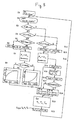
- Fig. 8 is a flow chart showing a control procedure of an embodiment.
- which has been captured in step 5 is compared with 2/ ⁇ 3 • Vmax.
- 2/ ⁇ 3 • Vmax is an output voltage at a vertex of the hexagon in Fig.
- step 6 the captured ⁇ 1 is converted to a value ranging from 0 to 60 degrees on the basis of a table shown in Fig. 9, and the value is set as ⁇ 11.
- step 15 t0, t1 and t2 are calculated on the basis of the corrected voltage amplitude command
- step 16 switching between DOWN mode and UP mode is effected.
- step 19 T0, T1, and T2 are set to TU, TV, and TW with reference to ⁇ 1 on the basis of the table shown in Fig. 9.
- step 20 TU, TV, and TW are output.
- a line voltage exceeding a direct current bus voltage of the PWM inverter can be output; simultaneously, an intermediate state ranging from a sinusoidal output to an output of six-step voltage (rectangular output) is developed, thereby enabling a smooth transition.
- the present invention has been conceived to solve the above problems and to provide a PWM inverter which enables smooth mode switching during transition from a sinusoidal voltage output to a six-step voltage output, and which can provide smooth mode switching by means of simple control processing.
- claim 1 of the invention is characterized by a PWM inverter having PWM pulse output means for outputting a PWM pulse signal upon magnitude comparison of phase voltage commands with a carrier wave of a triangular or a saw-tooth waveform, wherein:
- the line voltage can be output in a sinusoidal wave; and even in the case where the amplitude of the line voltage command exceeds the direct current bus voltage, the line voltage having the direct current bus voltage as an upper limit thereof can be output (in this case, the output voltage is not sinusoidal); accordingly, even a voltage output higher than the direct current bus voltage can be output as an amplitude of the line voltage command (when viewed as an effective value of a fundamental wave component).
- smooth transition switching can also be enabled with regard to a voltage amplitude of the phase voltage commands.
- the reason for this is that there are provided a first region of up to 1/ ⁇ 3 times a direct current bus voltage (when twice the value of the amplitude of the carrier wave is caused to correspond to the direct current bus voltage, the phase voltage commands is 2/ ⁇ 3 times the carrier amplitude, and the same applies hereinafter) which is capable of outputting a sinusoidal wave voltage; a third region of 2/ ⁇ 3 times the direct current bus voltage ⁇ where six-step voltage is output ⁇ or larger (4/ ⁇ 3 times the carrier amplitude or larger); and an intermediate second region thereof.
- the invention defined in claim 2 is characterized in that the PWM inverter of claim 1 includes first voltage conversion means which limits the amplitude of the phase voltage commands to 4/ ⁇ 3 times the amplitude of the carrier wave when the amplitude of the phase voltage commands is 4/ ⁇ 3 times an amplitude of the carrier wave or larger.
- the line voltage command (instantaneous value) is always equal to or greater than the direct current bus voltage.
- the invention defined in claim 3 is characterized in that the PWM inverter of claim 1 includes second voltage conversionmeans which limits the amplitudes of the phase voltage commands to a predetermined value of 4/ ⁇ 3 times the amplitude of the carrier wave or larger when the amplitudes of the phase voltage commands are 4/ ⁇ 3 times an amplitude of the carrier wave or larger.
- the invention defined in claim 4 is characterized in that the PWM inverter of claim 1 or claim 3 includes third voltage conversion means which converts the phase voltage commands to values obtained from multiplication of the phase voltage commands by ⁇ 3 when the amplitudes of the phase voltage commands are 2/ ⁇ 3 times an amplitude of the carrier wave or larger.
- a six-step voltage which serves as a maximum line voltage of the PWM inverter is 2/ ⁇ 3 times a direct current bus voltage (when viewed as an amplitude value of a fundamental wave component). Therefore, in the case where a six-step voltage output is enabled when voltage amplitudes of the line voltage commands in accordance with the phase voltage commands are 2 ⁇ 3 times the direct current bus voltage or larger; in other words, when the phase voltage commands (amplitude values) are 2/3 times the direct current bus voltage (the phase voltage commands are 4/3 times the carrier wave amplitude), the PWM inverter can output voltages which follow command voltages.
- phase voltage commands amplitude values
- the only requirement is to set as phase voltage commands values obtained by multiplication of the phase voltage commands by ⁇ 3.
- voltage conversionprocessing is performed only within a region where output of a sinusoidal voltage is impossible; in other words, a region where the amplitudes of the phase voltage commands are 2/ ⁇ 3 times the amplitude of the carrier wave or larger.
- first and third voltage conversion means are formed from voltage conversion means 1, which is set as fourth voltage conversion means.
- the invention defined in claim 6 is characterized in that the first voltage conversion means of the PWM inverter of claim 2 limits the amplitude of the phase voltage commands to 4/ ⁇ 3 times the amplitude of the carrier wave when the amplitudes of the line voltage obtained from the phase voltage commands are four times an amplitude of the carrier wave or larger.
- the invention defined in claim 7 is characterized in that the second voltage conversion means of the PWM inverter of claim 3 limits the amplitude of the phase voltage commands to a predetermined value of 4/ ⁇ 3 times the amplitude of the carrier wave or larger when the amplitude of the line voltage obtained from the phase voltage commands is four times an amplitude of the carrier wave or larger.
- the invention defined in claim 8 is characterized in that the third voltage conversion means of the PWM inverter of claim 4 converts the phase voltage values into values obtained from multiplication of the phase voltage values by ⁇ 3 when the amplitude of the line voltage obtained from the phase voltage commands is two times an amplitude of the carrier wave or larger.
- 1 denotes a voltage command shifter
- 2 denotes a PWM signal generator
- 3 denotes a carrier signal generator
- 4 denotes a voltage command limiter
- 5 denotes a voltage commandmultiplier
- 11 denotes a commercial power source
- 12 denotes a rectifier diode in a converter section
- 13 through 18 denote IGBT transistors
- 19 through 24 denote circulating diodes
- 25 denotes a current detector
- 26 denotes an electric motor
- 29 denotes a smoothing capacitor
- 101 denotes a PWM pattern generation section
- 102 denotes a first voltage command limiter
- 103 denotes a second voltage command limiter
- 104 denotes a voltage-command-limiting-value switching section
- 105 denotes a mode determination section.
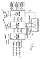
- Fig. 1 is a block diagram of a first embodiment of the present invention.
- 1 denotes a voltage command shifter; 2 denotes a PWM generator; and 3 denotes a carrier signal generator.
- the voltage command shifter 1 compares absolute values (
- the PWM signal generator 2 compares a carrier wave from the carrier signal generator 3 with Vu, Vv, and Vw, thereby outputting PWM pulses of the respective phases.
- a sinusoidal wave is generally used for three-phase voltage commands supplied from a high-level controller; however, when a line voltage is designed so as to output a desired voltage, other waveforms may also be employed instead.
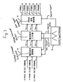
- Fig. 2 is a block diagram of a second embodiment of the present invention.
- 1 denotes a voltage command shifter
- 2 denotes a PWM generator
- 3 denotes a carrier signal generator
- 4 denotes a voltage command limiter.
- the voltage command limiter 4 obtains a voltage amplitude of the phase voltage commands, and obtains an amplitude of carrier signals from the maximum value and the minimum value of the carrier signals from the carrier signal generator 3; and the amplitude of the phase voltage commands having an upper limit of 4/ ⁇ 3 times the amplitude of the carrier signals is supplied to the voltage command shifter 1.
- the voltage commands can be prevented from becoming excessively large; accordingly, a control response speed of the PWM inverter under a condition where the voltage commands must be decreased rapidly is improved.
- the voltage amplitude of the phase voltage command has been described as being obtained in the voltage command limiter 4; however, there may be adopted a configuration where an amplitude of the phase voltage commands is supplied from a high-level controller to the voltage command limiter 4. Further, no problem arises in integrating the voltage command limiter 4 into the voltage command shifter 1.
- Fig. 3 is a block diagram of a third embodiment of the present invention.
- 1 denotes a voltage command shifter
- 2 denotes a PWM generator
- 3 denotes a carrier signal generator
- 5 denotes a voltage command multiplier.
- the voltage command multiplier 5 obtains an amplitude Vpp of the phase voltage commands, thereby obtaining a maximum carrier signal value Cmax, a minimum value Cmin, and a differential value thereof Cdiff.
- Vu', Vv', and Vw' values (Vu', Vv', and Vw') ⁇ which are obtained from multiplication of the respective phase voltage command values (Vru, Vrv, and Vrv) by ⁇ 3 ⁇ are supplied to the voltage command shifter 1.
- multiplication is performedby the voltage command multiplier 5; however, such a multiplication adjustment can be performed elaborately by a high-level controller.
- a high-level controller When the above is adopted, linearity of voltage values which are actually output from the PWM inverter and voltage commands is further improved.
- the voltage command multiplier 5 may be integrated in the voltage command shifter 1.
- the second embodiment and the third embodiment can be implemented in a combined manner.
- the present invention is based on Japanese Patent Application filedonMarch20, 2002 (Japanese PatentApplication No.2002-078452), which is incorporated herein by reference.
- the present invention provides smooth mode switching during a transition from a sinusoidal voltage output to a six-step voltage output; and even in a current control system where current control function is required, favorable and stable control function can be obtained during the above transition.
- the invention does not require complicated processing including determination of switching, limitation on lengths of command voltage vectors, or correction of angles of vectors by calculating an arcsine and using a table which stores lengths of vectors and angles corresponding thereto; and such transition switching can be implemented rapidly through simple processing.
Landscapes
- Engineering & Computer Science (AREA)
- Power Engineering (AREA)
- Inverter Devices (AREA)
Abstract
Description
when the amplitudes of the phase voltage commands are 2/√3 times an amplitude of the carrier wave or larger.
the respective voltage commands are output as signals (Vu, Vv, and Vw) for the
Claims (8)
- A PWM inverter having PWM pulse output means for outputting a PWM pulse signal upon magnitude comparison of phase voltage commands with a carrier wave of a triangular or a saw-tooth waveform, wherein:a maximum phase whose absolute value is the maximum among those of phase voltage command is selected; in the case where the phase voltage commands of said maximum phase are larger than a maximum value of said carrier wave, a difference obtained from subtraction of said maximum value of said carrier wave from phase voltage commands of said maximum phase is set as a first differential; said first differential is subtracted from said phase voltage commands of said respective phases; and these subtraction results are set as phase output voltage commands of said respective phases;in the case where said the phase voltage commands of said maximum phase are smaller than a minimum value of said carrier wave, a difference obtained from subtraction of said minimum value of said carrier wave from phase voltage command of said maximum phase is set as a second differential; said second differential is subtracted from said phase voltage commands of said respective phases; and these subtraction results are set as phase output voltage commands of said respective phases; andin a case other than above, phase voltage commands are set as phase output voltage commands as they are;the PWM inverter characterized by comprising voltage command processing means for outputting said phase output voltage commands to said PWM pulse output means upon input of phase voltage commands.
- The PWM inverter according to claim 1, characterized by having first voltage conversion means for limiting an amplitude of said phase voltage commands to 4/√3 times the amplitude of said carrier wave when the amplitude of said phase voltage commands is 4/√3 times an amplitude of said carrier wave or larger.
- The PWM inverter according to claim 1, characterized by having second voltage conversion means for limiting the amplitude of said phase voltage commands to a predetermined value which is 4/√3 times an amplitude of said carrier wave or larger when the amplitude of said phase voltage commands is 4/√3 times the amplitude of said carrier wave or larger.
- The PWM inverter according to claim 1 or 3, characterized by having third voltage conversion means for converting said phase voltage commands to a value obtained from multiplication of said phase voltage commands by √3 when the amplitude of said phase voltage commands is 2/√3 times the amplitude of said carrier wave or larger.
- The PWM inverter of claims 2 and 4, or the PWM inverter of claims 3 and 4, characterized in that the first and third voltage conversion means, or the second and third voltage conversion means are constituted of single voltage conversion means; and the single voltage conversionmeans is taken as fourth voltage conversion means.
- The PWM inverter according to claim 2, characterized in that, said first voltage conversionmeans limits the amplitude of said phase voltage commands to 4/√3 times an amplitude of said carrier wave when an amplitude of a line voltage obtained from saidphase voltage commands becomes four times the amplitude of said carrier wave or larger.
- The PWM inverter according to claim 3, characterized in that said secondvoltage conversionmeans limits the amplitude of said phase voltage commands to a predetermined value of 4/√3 times the amplitude of said carrier wave or larger when an amplitude of a line voltage obtained from said phase voltage commands becomes four times the amplitude of said carrier wave or larger.
- The PWM inverter according to claim 4, characterized in that said third voltage conversion means converts said phase voltage commands into values obtained from multiplication of said phase voltage commands by √3 when an amplitude of a line voltage obtained from said phase voltage commands becomes two times the amplitude of said carrier wave or larger.
Applications Claiming Priority (3)
| Application Number | Priority Date | Filing Date | Title |
|---|---|---|---|
| JP2002078452 | 2002-03-20 | ||
| JP2002078452A JP3841282B2 (en) | 2002-03-20 | 2002-03-20 | PWM inverter device |
| PCT/JP2003/003267 WO2003079531A1 (en) | 2002-03-20 | 2003-03-18 | Pwm inverter device |
Publications (3)
| Publication Number | Publication Date |
|---|---|
| EP1487093A1 true EP1487093A1 (en) | 2004-12-15 |
| EP1487093A4 EP1487093A4 (en) | 2007-05-09 |
| EP1487093B1 EP1487093B1 (en) | 2012-08-08 |
Family
ID=28035584
Family Applications (1)
| Application Number | Title | Priority Date | Filing Date |
|---|---|---|---|
| EP03712751A Expired - Lifetime EP1487093B1 (en) | 2002-03-20 | 2003-03-18 | Pwm inverter device |
Country Status (6)
| Country | Link |
|---|---|
| US (1) | US7068526B2 (en) |
| EP (1) | EP1487093B1 (en) |
| JP (1) | JP3841282B2 (en) |
| KR (1) | KR20040098016A (en) |
| CN (1) | CN100438302C (en) |
| WO (1) | WO2003079531A1 (en) |
Cited By (1)
| Publication number | Priority date | Publication date | Assignee | Title |
|---|---|---|---|---|
| EP2204901A4 (en) * | 2007-10-24 | 2017-05-03 | Daikin Industries, Ltd. | Power conversion device |
Families Citing this family (32)
| Publication number | Priority date | Publication date | Assignee | Title |
|---|---|---|---|---|
| US8189356B2 (en) * | 2006-04-06 | 2012-05-29 | Kabushiki Kaisha Yaskawa Denki | PWM inverter |
| CN103051203B (en) * | 2006-04-20 | 2015-11-04 | 大金工业株式会社 | The control method of power inverter and power inverter |
| JP4957303B2 (en) * | 2007-03-14 | 2012-06-20 | 株式会社明電舎 | Space vector modulation method for AC-AC direct conversion device |
| DE102007040560A1 (en) * | 2007-08-28 | 2009-03-12 | Continental Automotive Gmbh | Method for controlling an inverter and associated device |
| JP4591597B2 (en) * | 2008-08-01 | 2010-12-01 | 株式会社デンソー | Multiphase AC synchronous motor drive device |
| JP4748245B2 (en) * | 2009-04-10 | 2011-08-17 | 株式会社デンソー | Rotating machine control device |
| CN102474192B (en) * | 2009-08-26 | 2014-09-10 | 大金工业株式会社 | Power conversion device and control method thereof |
| CN102111125B (en) * | 2009-12-28 | 2015-04-22 | 北京普源精电科技有限公司 | Signal generator with current output type amplifying unit |
| WO2013067429A1 (en) * | 2011-11-03 | 2013-05-10 | Arraypower, Inc. | Direct current to alternating current conversion utilizing intermediate phase modulation |
| US8619446B2 (en) * | 2012-04-27 | 2013-12-31 | Rockwell Automation Technologies, Inc. | Cascaded H-bridge (CHB) inverter level shift PWM with rotation |
| US9007787B2 (en) | 2012-08-13 | 2015-04-14 | Rockwell Automation Technologies, Inc. | Method and apparatus for bypassing Cascaded H-Bridge (CHB) power cells and power sub cell for multilevel inverter |
| US9425705B2 (en) | 2012-08-13 | 2016-08-23 | Rockwell Automation Technologies, Inc. | Method and apparatus for bypassing cascaded H-bridge (CHB) power cells and power sub cell for multilevel inverter |
| US9724997B2 (en) | 2012-09-07 | 2017-08-08 | Ford Global Technologies, Llc | Electric motor temperature compensation |
| JP5652454B2 (en) * | 2012-09-28 | 2015-01-14 | 株式会社安川電機 | Power converter |
| US9240731B2 (en) | 2013-03-18 | 2016-01-19 | Rockwell Automation Technologies, Inc. | Power cell bypass method and apparatus for multilevel inverter |
| US9083230B2 (en) | 2013-06-20 | 2015-07-14 | Rockwell Automation Technologies, Inc. | Multilevel voltage source converters and systems |
| US9520800B2 (en) | 2014-01-09 | 2016-12-13 | Rockwell Automation Technologies, Inc. | Multilevel converter systems and methods with reduced common mode voltage |
| US9325252B2 (en) | 2014-01-13 | 2016-04-26 | Rockwell Automation Technologies, Inc. | Multilevel converter systems and sinusoidal pulse width modulation methods |
| JP6295809B2 (en) * | 2014-04-28 | 2018-03-20 | 株式会社安川電機 | Power conversion device, control device, and control method for power conversion device |
| US9407178B2 (en) | 2014-11-14 | 2016-08-02 | GM Global Technology Operations LLC | Method and apparatus for controlling an electric machine in a six-step mode |
| US9419549B2 (en) * | 2014-11-14 | 2016-08-16 | GM Global Technology Operations LLC | Method and apparatus for controlling an electric machine in a six-step mode |
| US9559541B2 (en) | 2015-01-15 | 2017-01-31 | Rockwell Automation Technologies, Inc. | Modular multilevel converter and charging circuit therefor |
| US9748862B2 (en) | 2015-05-13 | 2017-08-29 | Rockwell Automation Technologies, Inc. | Sparse matrix multilevel actively clamped power converter |
| KR101779698B1 (en) | 2016-02-18 | 2017-09-18 | 엘에스산전 주식회사 | Method and apparatus for generating pwm signal |
| CN105897106B (en) * | 2016-04-10 | 2018-08-21 | 北京工业大学 | A kind of increasing journey system starting method of permanent magnet synchronous motor using hall position sensor |
| US9812990B1 (en) | 2016-09-26 | 2017-11-07 | Rockwell Automation Technologies, Inc. | Spare on demand power cells for modular multilevel power converter |
| CN106787915B (en) * | 2017-01-06 | 2019-04-16 | 南京理工大学 | Dual-carrier SVPWM control method for suppressing circulating current of energy feedback device |
| JP7070004B2 (en) * | 2018-04-13 | 2022-05-18 | 株式会社安川電機 | Power conversion device and power conversion method |
| US10158299B1 (en) * | 2018-04-18 | 2018-12-18 | Rockwell Automation Technologies, Inc. | Common voltage reduction for active front end drives |
| US11211879B2 (en) | 2019-09-23 | 2021-12-28 | Rockwell Automation Technologies, Inc. | Capacitor size reduction and lifetime extension for cascaded H-bridge drives |
| US11342878B1 (en) | 2021-04-09 | 2022-05-24 | Rockwell Automation Technologies, Inc. | Regenerative medium voltage drive (Cascaded H Bridge) with reduced number of sensors |
| CN114157170B (en) * | 2021-11-26 | 2023-07-07 | 华南理工大学 | Model predictive power control method for T-type three-level rectifier based on sliding mode control |
Family Cites Families (11)
| Publication number | Priority date | Publication date | Assignee | Title |
|---|---|---|---|---|
| JPH0746918B2 (en) * | 1987-06-03 | 1995-05-17 | 株式会社日立製作所 | Power converter |
| JPH0793823B2 (en) * | 1988-02-01 | 1995-10-09 | 株式会社日立製作所 | PWM controller for voltage source inverter |
| JPH04133667A (en) | 1990-09-21 | 1992-05-07 | Toyota Motor Corp | Voltage type pwm inverter |
| US5153821A (en) * | 1991-09-06 | 1992-10-06 | Otis Elevator Company | Pulse-width-modulation method for providing extended linearity, reduced commutation losses and increase in inverter/converter output voltage |
| US5610806A (en) * | 1995-06-19 | 1997-03-11 | Allen-Bradley Company, Inc. | Pulse width modulation method for driving three phase power inverter/converter switches with balanced discontinuous phase commands |
| US5790396A (en) * | 1995-12-19 | 1998-08-04 | Kabushiki Kaisha Toshiba | Neutral point clamped (NPC) inverter control system |
| JP3781069B2 (en) | 1997-03-14 | 2006-05-31 | 株式会社安川電機 | Inverter control method and apparatus |
| JP2001218479A (en) | 2000-01-28 | 2001-08-10 | Yaskawa Electric Corp | PWM controller |
| JP3666432B2 (en) * | 2001-09-20 | 2005-06-29 | 株式会社デンソー | Power converter and multiphase load drive control method |
| JP4045105B2 (en) * | 2002-01-30 | 2008-02-13 | 株式会社日立産機システム | Pulse width modulation method, power conversion device, and inverter device |
| US6842354B1 (en) * | 2003-08-08 | 2005-01-11 | Rockwell Automation Technologies, Inc. | Capacitor charge balancing technique for a three-level PWM power converter |
-
2002
- 2002-03-20 JP JP2002078452A patent/JP3841282B2/en not_active Expired - Fee Related
-
2003
- 2003-03-18 KR KR10-2004-7014806A patent/KR20040098016A/en not_active Ceased
- 2003-03-18 US US10/508,084 patent/US7068526B2/en not_active Expired - Fee Related
- 2003-03-18 WO PCT/JP2003/003267 patent/WO2003079531A1/en not_active Ceased
- 2003-03-18 CN CNB038062798A patent/CN100438302C/en not_active Expired - Fee Related
- 2003-03-18 EP EP03712751A patent/EP1487093B1/en not_active Expired - Lifetime
Cited By (1)
| Publication number | Priority date | Publication date | Assignee | Title |
|---|---|---|---|---|
| EP2204901A4 (en) * | 2007-10-24 | 2017-05-03 | Daikin Industries, Ltd. | Power conversion device |
Also Published As
| Publication number | Publication date |
|---|---|
| JP2003284350A (en) | 2003-10-03 |
| CN1643769A (en) | 2005-07-20 |
| EP1487093A4 (en) | 2007-05-09 |
| US7068526B2 (en) | 2006-06-27 |
| US20050128777A1 (en) | 2005-06-16 |
| CN100438302C (en) | 2008-11-26 |
| JP3841282B2 (en) | 2006-11-01 |
| WO2003079531A1 (en) | 2003-09-25 |
| KR20040098016A (en) | 2004-11-18 |
| EP1487093B1 (en) | 2012-08-08 |
Similar Documents
| Publication | Publication Date | Title |
|---|---|---|
| US7068526B2 (en) | PWM inverter device | |
| CN101814851B (en) | Pwm rectifier | |
| US9013906B2 (en) | Power system-interconnected inverter device | |
| US10374503B2 (en) | Power conversion device | |
| KR20160122923A (en) | Apparatus and method for generating offset voltage of 3-phase inverter | |
| CN101421911A (en) | Power conversion device and control method for power conversion device | |
| CN104682761A (en) | Current source power conversion apparatus | |
| JP6676830B1 (en) | Power converter | |
| JPH03107373A (en) | Power converter and control method thereof | |
| US12562654B2 (en) | Power conversion device | |
| JP2006109541A (en) | Control device for power converter | |
| JP2007110811A (en) | Inverter device and control method thereof | |
| JP6754022B1 (en) | Power converter | |
| JP7202244B2 (en) | power converter | |
| JP3781069B2 (en) | Inverter control method and apparatus | |
| JPH09163755A (en) | Power converter control device | |
| JP3051844B2 (en) | PWM method and apparatus for three-phase voltage source inverter | |
| JP7356395B2 (en) | power converter | |
| JP2019201493A (en) | Multilevel power conversion device and control method therefor | |
| JP2008109790A (en) | Power converter | |
| JPH05211775A (en) | Inverter device | |
| JP4140479B2 (en) | Inverter control method | |
| JP2005012857A (en) | Power converter | |
| JPH03235671A (en) | Circulating current suppression method for parallel multiple inverters and parallel multiple inverters | |
| JPH0956165A (en) | PWM controller |
Legal Events
| Date | Code | Title | Description |
|---|---|---|---|
| PUAI | Public reference made under article 153(3) epc to a published international application that has entered the european phase |
Free format text: ORIGINAL CODE: 0009012 |
|
| 17P | Request for examination filed |
Effective date: 20040910 |
|
| AK | Designated contracting states |
Kind code of ref document: A1 Designated state(s): AT BE BG CH CY CZ DE DK EE ES FI FR GB GR HU IE IT LI LU MC NL PT RO SE SI SK TR |
|
| A4 | Supplementary search report drawn up and despatched |
Effective date: 20070411 |
|
| REG | Reference to a national code |
Ref country code: DE Ref legal event code: R079 Ref document number: 60341739 Country of ref document: DE Free format text: PREVIOUS MAIN CLASS: H02M0007480000 Ipc: H02M0007538700 |
|
| GRAP | Despatch of communication of intention to grant a patent |
Free format text: ORIGINAL CODE: EPIDOSNIGR1 |
|
| RIC1 | Information provided on ipc code assigned before grant |
Ipc: H02M 7/483 20070101ALI20120206BHEP Ipc: H02M 7/5387 20070101AFI20120206BHEP |
|
| GRAS | Grant fee paid |
Free format text: ORIGINAL CODE: EPIDOSNIGR3 |
|
| GRAA | (expected) grant |
Free format text: ORIGINAL CODE: 0009210 |
|
| AK | Designated contracting states |
Kind code of ref document: B1 Designated state(s): DE |
|
| REG | Reference to a national code |
Ref country code: DE Ref legal event code: R096 Ref document number: 60341739 Country of ref document: DE Effective date: 20121011 |
|
| PLBE | No opposition filed within time limit |
Free format text: ORIGINAL CODE: 0009261 |
|
| STAA | Information on the status of an ep patent application or granted ep patent |
Free format text: STATUS: NO OPPOSITION FILED WITHIN TIME LIMIT |
|
| 26N | No opposition filed |
Effective date: 20130510 |
|
| REG | Reference to a national code |
Ref country code: DE Ref legal event code: R097 Ref document number: 60341739 Country of ref document: DE Effective date: 20130510 |
|
| PGFP | Annual fee paid to national office [announced via postgrant information from national office to epo] |
Ref country code: DE Payment date: 20160315 Year of fee payment: 14 |
|
| REG | Reference to a national code |
Ref country code: DE Ref legal event code: R119 Ref document number: 60341739 Country of ref document: DE |
|
| PG25 | Lapsed in a contracting state [announced via postgrant information from national office to epo] |
Ref country code: DE Free format text: LAPSE BECAUSE OF NON-PAYMENT OF DUE FEES Effective date: 20171003 |