EP1484764A1 - Method for generating a reference current for sense amplifiers connected to cells of a memory matrix, particularly in big-sized flash memories, and corresponding generator - Google Patents
Method for generating a reference current for sense amplifiers connected to cells of a memory matrix, particularly in big-sized flash memories, and corresponding generator Download PDFInfo
- Publication number
- EP1484764A1 EP1484764A1 EP03425353A EP03425353A EP1484764A1 EP 1484764 A1 EP1484764 A1 EP 1484764A1 EP 03425353 A EP03425353 A EP 03425353A EP 03425353 A EP03425353 A EP 03425353A EP 1484764 A1 EP1484764 A1 EP 1484764A1
- Authority
- EP
- European Patent Office
- Prior art keywords
- ref
- bit
- digital
- reference current
- signal
- Prior art date
- Legal status (The legal status is an assumption and is not a legal conclusion. Google has not performed a legal analysis and makes no representation as to the accuracy of the status listed.)
- Granted
Links
Images


Classifications
-
- G—PHYSICS
- G11—INFORMATION STORAGE
- G11C—STATIC STORES
- G11C16/00—Erasable programmable read-only memories
- G11C16/02—Erasable programmable read-only memories electrically programmable
- G11C16/06—Auxiliary circuits, e.g. for writing into memory
- G11C16/26—Sensing or reading circuits; Data output circuits
- G11C16/28—Sensing or reading circuits; Data output circuits using differential sensing or reference cells, e.g. dummy cells
-
- G—PHYSICS
- G11—INFORMATION STORAGE
- G11C—STATIC STORES
- G11C7/00—Arrangements for writing information into, or reading information out from, a digital store
- G11C7/14—Dummy cell management; Sense reference voltage generators
Definitions
- the present invention relates to a method for generating a reference current for sense amplifiers connected to cells of a memory matrix.
- the invention relates to a method for generating a reference current for sense amplifiers connected to cells of a memory matrix comprising a generation step of a first analogue reference current signal by means of a reference cell.
- the invention also relates to a reference current generator for sense amplifiers connected to cells of a memory matrix, said generator being connected to a reference cell effective to provide an analogue reference current signal.
- the invention particularly relates, but not exclusively, to a generation method to be used in reading operations on memory cells comprised in big-sized Flash memories and the following description is made with reference to this field of application for convenience of illustration only.
- a reading operation of a Flash memory cell comprised in a big-sized Flash memory requires a reading current passing through the cell to be compared with a current, called reference current, so as to determine if the read cell is a logic "1" or "0".
- the digital value allocated to the read cell is 1 respectively 0.
- the so-obtained digital value is thus the information stored in the read cell.
- reference current value is obtained by means of a Flash memory cell, called reference cell, which is programmed so as to have a reading current value being exactly median between the reading current values of a programmed cell and of an erased cell.
- This mean reading current value is transferred by means of a current mirror to all reading comparators or sense amplifiers comprised in a memory cell reading device associated to the Flash memory.
- the mean reading current value is particularly used as decision threshold by the sense amplifier in order to determine the digital value stored in the read cells, as schematically shown in figure 1.
- this figure schematically shows a portion 10 of a Flash memory architecture comprising a sense amplifier 11 connected to a memory cell 12 of a memory matrix 1, this cell 12 corresponding to a selected bitline 2 and wordline 3 and being also indicated as matrix cell.
- the sense amplifier 11 is also connected, through a current mirror 13, to a reference cell 14, always of the Flash type, having in turn a control terminal connected to a reference wordline 15.
- the current mirror 13 comprises a first mirror transistor M1 connected to the reference cell 14 as well as a plurality of second mirror transistors Mn connected to each one of the sense amplifiers 11 being provided in the Flash memory.
- the first mirror transistor M1 is connected through a line Ref_mirror to the plurality of sense amplifiers 11.
- the sense amplifier 11 compares a value of a reference current Irif provided by the reference cell 14 with a value of a cell current Icell passing through the selected matrix cell 12 and it provides on an output terminal OUT of the sense amplifier 11 a digital value corresponding to the content of the matrix cell 12.
- Flash reference cell for generating the reference current ensures a same dependence with respect to process, temperature and supply voltage changes of the reference current and the cell current.
- the reference current distribution along the whole memory cell matrix causes problems linked to parasitic effects.
- the sole line Ref_mirror is connected to a large number of sense amplifiers concerning it.
- the number of these sense amplifiers 11 is further increased in recent construction Flash memories in order to meet speed requirements needed by burst reading operations and to perform simultaneously writing and reading operations.
- the physical path of the line Ref_mirror is very long.
- this figure 2 schematically shows these undesired effects, i.e. the high capacitance value 21 in the node XRF, the high sensitivity to couplings 22 and noises 23.
- the line Rif_mirror is actually an analogue line and thus very sensitive to couplings and noise on a memory device supply line.
- memory devices using a single reference cell reading architecture as the one shown in figure 1, have a safety margin for reading operations performed on their cells being lower than the desired margin and they can even have reading errors.
- the reference cell consumes currents during its operation and, necessarily, it must be turned off when the memory device is in a stand-by condition.
- the reactivation operation is however obstructed by the high parasitic load associated to the node XRF.
- the technical problem underlying the present invention is to provide a method for generating a current value for a reference line of a memory device, particularly of the Flash type, to be used during reading operations of the cells comprised therein and a corresponding circuit architecture having such structural and functional characteristics as to allow a reference current to be generated and transmitted with a low sensitivity to couplings and noises, thus overcoming the limits and drawbacks still affecting memory devices according to the prior art.
- the solution idea underlying the present invention is to use an analog-to-digital conversion to transmit a reference current from a reference cell to the memory device sense amplifiers.
- the present invention relates to a method for generating a reference current for a reference line effective to be connected to a memory device, particularly of the Flash type.
- a reference current is obtained through a reference cell, advantageously of the Flash type, and it must be applied to a plurality of sense amplifiers associated to a reading architecture of the memory device.
- elements being structurally and functionally identical to elements already described with reference to the prior art will be given the same numeral references.
- the method according to the invention provides that the reference current REF is digitally coded by applying a convenient sampling thereof, as schematically shown in figure 3 showing, by way of example, a 4-bit Analog-to-Digital conversion with quantization on 16 possible levels for the reference current Irif considered in the range from 5uA to 27.5uA with a pitch of 1.5uA.
- figure 3 shows a straight line A corresponding to the analogue values that can be taken by the reference current for memory cell reading operations and a stepped line B corresponding to the approximate reference current values obtained through a 4-bit Analog-to-Digital conversion.
- the reference cell current value is completely defined by a 4-bit digital signal REF_BIT[3:0] obtained from the Analog-to-Digital conversion.
- This digital signal REF_BIT[3:0] is then sent through a digital line to corresponding Digital-to-Analog conversion blocks to obtain the required reference current value REF1 to be applied to sense amplifiers 11 to perform the reading operations of the memory cells connected thereto.
- this digital signal REF_BIT[3:0] obtained from the conversion of the analogue value REF of the reference current is free from noises and couplings, eliminating all stability problems of the analogue line REF_MIRROR and noise effect affecting prior art devices.
- Analog-to-Digital conversion operations A2D are added to obtain the digital signal REF_BIT[3:0] corresponding to the reference current analogue signal REF coding of the reference cell 14, as well as Digital-to-Analog conversion operations D2A to reconstruct, starting from the coded value thereof, the digital signal REF_BIT[3:0], an analogue value REF1 of the reading reference current to be applied to sense amplifiers 11.
- the method for generating a reference current for sense amplifiers connected to matrix cells of a memory device comprises the following steps:
- sense amplifiers 11 can operate as in known memory devices, comparing this reference current analogue signal REF1 with the reading currents Icell of the matrix cells 12 connected thereto in order to determine the logic content.
- the method according to the invention is thus extremely advantageous with respect to known methods since it is free from errors caused by couplings and parasitic capacitance, though being still subject to a slight quantization error having a highest value being known a priori.
- a reference current generator effective to implement the method according to the invention is schematically shown in figure 4, globally indicated with 40.
- the generator 40 is connected between a reference cell 14 effective to provide a reference current analogue signal REF and at least a sense amplifier 11 effective to receive a reference current analogue signal REF1 to perform comparison operations with a reading current signal Icell passing through a matrix cell 12 connected thereto.
- the generator 40 comprises, in cascade connection, an Analog-to-Digital conversion block 41 to perform the conversion of the analogue signal REF connected to a measure and logic calculation block 42, connected in turn to a digital line 43 whereon the reference current conversion digital signal REF_BIT[3:0] is sent.
- the measure and logic calculation block 42 allows a periodical updating of the digital signal REF_BIT[3:0] to be implemented, as it will be explained hereafter.
- the digital line 43 is connected to a Digital-to-Analog conversion block 44 to perform the conversion of the digital signal REF_BIT[3:0] into the reference current analogue signal REF1 to be applied to the sense amplifiers 11.
- the digital line 43 is free from the effects linked to the capacitive values 45 and to the couplings 46 affecting the line REF_MIRROR used to transfer to sense amplifiers 11 the reference current in prior art devices.
- the generator 40 provides a first 47 and second 48 dedicated lines connected to conversion blocks 41 and 44.
- the first dedicated line 47 provides conversion blocks 41 and 44 with a voltage reference, particularly a ground Gnd_ref, while the second dedicated line 48 provides these blocks with a reference signal BGAP of the Band-Gap type obtained by means of a convenient Band-Gap generator 48A.
- a memory device 50 equipped with a single reference cell reading architecture is thus obtained, as schematically shown in figure 5.
- the memory device 50 comprises a memory cell matrix 1 wherein a memory cell 12 is selected through a bitline 2 and a wordline 3.
- the memory device 50 comprises a reference current generator 40 connected between a reference cell 14 and the sense amplifiers 11 and manufactured as previously indicated.
- the method for generating a reference current according to the invention provides that conversion processes A2D and D2A are periodically performed, even when the memory device is in the stand-by condition.
- the updating frequency can be set at about one update per second, in order to pursue environmental temperature changes and also bias changes (for example battery voltage changes in mobile applications).
- Such an updating frequency is does not involve considerable increases in the memory device stand-by current but only negligible current increases caused by turning on a dedicated circuit performing the updating of conversion processes.
- Figure 6 schematically shows, globally indicated with 60, an updating circuit of the reference current digital signal REF_BIT[3:0].
- the updating circuit 60 essentially comprises a state machine REF_UPDATE.
- the updating circuit 60 is connected between a corresponding sense amplifier 11 of the memory device and the line 43 of the digital signal REF_BIT[3:0].
- the sense amplifiers 11 and the state machine REF_UPDATE as a whole form the measure and logic calculation block 42 indicated in figure 4.
- the sense amplifier 11 is connected to the Digital-to-Analog D2A conversion block 44 and to a reference cell 14.
- the conversion D2A block 44 is input a digital signal REF_BIT[3:0] coming from the updating circuit 60 and it provides a reconstructed current analogue circuit REF2.
- the reference cell 14 is periodically read with the sense amplifier 11, which compares the reference current obtained from the reference cell 14 with the current analogue signal REF2 obtained from the conversion D2A block 44.
- the digital signal BIT[3:0] being input at the conversion D2A block 44 is generated by the state machine REF_UPDATE comprised in the updating circuit 60.
- this state machine REF_UPDATE increases or decreases the digital signal BIT[3:0] until a signal SOUT being output from the sense amplifier 11 does not commute.
- the digital signal BIT[3:0] is sent on the line 43 and allocated as value of the digital signal REF_BIT[3:0] to be sent to sense amplifiers 11.
- the updating circuit 60 turns the reference cell 14 on and it updates the value of the digital signal REF_BIT[3:0] on the line 43.
- Analog-to-Digital conversion A2D performed on the current of the reference cell 67 of the updating circuit 60 is performed by using the same structures (sense amplifier 11 and Digital-to-Analog conversion block 44 globally indicated with 61 in figure 6) existing in the memory device, thus eliminating errors caused by different modes of performing a reference measurement.
- the current generator implementing the method according to the invention is free from noises and couplings.
- the digital signal corresponding to the reference current is always available (no setup time at the first reading after a stand-by) and it is periodically updated to take into consideration the temperature and supply voltage time changes.
- the updating frequency is such as not to considerably weigh on the stand-by consumption.
- the only error introduced is a quantization error linked to conversion processes A2D and D2A, whose highest value is however known a priori. It is worth noting that this quantization error can be reduced for example by increasing the number of bits coding the current analogue signal.
Landscapes
- Read Only Memory (AREA)
Abstract
- generating a first reference current analogue signal (REF) through a reference cell (14).
- performing an Analog-to-Digital conversion of the first analogue signal (REF) into a reference current digital signal (REF_BIT[3:0]);
- sending the digital signal (REF_BIT[3:0]) on a connection line (43) to the sense amplifiers (11); and
- performing a Digital-to-Analog conversion of the digital signal (REF_BIT[3:0]) into a second reference current analogue signal (REF1) to be applied as reference current (Iref) to the sense amplifiers (11).
Description
- The present invention relates to a method for generating a reference current for sense amplifiers connected to cells of a memory matrix.
- More specifically, the invention relates to a method for generating a reference current for sense amplifiers connected to cells of a memory matrix comprising a generation step of a first analogue reference current signal by means of a reference cell.
- The invention also relates to a reference current generator for sense amplifiers connected to cells of a memory matrix, said generator being connected to a reference cell effective to provide an analogue reference current signal.
- The invention particularly relates, but not exclusively, to a generation method to be used in reading operations on memory cells comprised in big-sized Flash memories and the following description is made with reference to this field of application for convenience of illustration only.
- As it is well known, a reading operation of a Flash memory cell comprised in a big-sized Flash memory requires a reading current passing through the cell to be compared with a current, called reference current, so as to determine if the read cell is a logic "1" or "0".
- In particular, if the higher cell reading current respectively lower than the reference current, the digital value allocated to the read cell is 1 respectively 0.
- The so-obtained digital value is thus the information stored in the read cell.
- It is also known that in traditional Flash memories the reference current value is obtained by means of a Flash memory cell, called reference cell, which is programmed so as to have a reading current value being exactly median between the reading current values of a programmed cell and of an erased cell.
- This mean reading current value is transferred by means of a current mirror to all reading comparators or sense amplifiers comprised in a memory cell reading device associated to the Flash memory. The mean reading current value is particularly used as decision threshold by the sense amplifier in order to determine the digital value stored in the read cells, as schematically shown in figure 1.
- In particular, this figure schematically shows a
portion 10 of a Flash memory architecture comprising asense amplifier 11 connected to amemory cell 12 of amemory matrix 1, thiscell 12 corresponding to aselected bitline 2 andwordline 3 and being also indicated as matrix cell. - The
sense amplifier 11 is also connected, through acurrent mirror 13, to areference cell 14, always of the Flash type, having in turn a control terminal connected to areference wordline 15. In particular, thecurrent mirror 13 comprises a first mirror transistor M1 connected to thereference cell 14 as well as a plurality of second mirror transistors Mn connected to each one of thesense amplifiers 11 being provided in the Flash memory. The first mirror transistor M1 is connected through a line Ref_mirror to the plurality ofsense amplifiers 11. - As seen, the
sense amplifier 11 compares a value of a reference current Irif provided by thereference cell 14 with a value of a cell current Icell passing through theselected matrix cell 12 and it provides on an output terminal OUT of the sense amplifier 11 a digital value corresponding to the content of thematrix cell 12. - It is worth noting that the use of a Flash reference cell for generating the reference current ensures a same dependence with respect to process, temperature and supply voltage changes of the reference current and the cell current.
- In the case of high density Flash memories, the reference current distribution along the whole memory cell matrix causes problems linked to parasitic effects. In fact, the sole line Ref_mirror is connected to a large number of sense amplifiers concerning it. The number of these
sense amplifiers 11 is further increased in recent construction Flash memories in order to meet speed requirements needed by burst reading operations and to perform simultaneously writing and reading operations. - Moreover, with big-sized memory devices, the physical path of the line Ref_mirror is very long.
- These two conditions both produce a high capacitance value in a connection node XRF between the first mirror transistor M1 and the plurality of second mirror transistors Mn in
sense amplifiers 11 and thus a high sensitivity to couplings and noises in the Flash memory device, as schematically shown in figure 2. - In particular, this figure 2 schematically shows these undesired effects, i.e. the
high capacitance value 21 in the node XRF, the high sensitivity tocouplings 22 andnoises 23. - In such conditions, couplings with variable signals, such as a clock signal and the signal on a data bus associated to the memory device, as well as noises caused by local changes of a supply voltage and mainly the high parasitic capacitance caused by the signal path length in big-sized devices, such as the conductive paths between the reference cell and sense amplifiers, actually cause a reading error which turns out in sense amplifiers as a reading with a reference current being different from the theoretical current.
- The line Rif_mirror is actually an analogue line and thus very sensitive to couplings and noise on a memory device supply line.
- In other words, memory devices using a single reference cell reading architecture, as the one shown in figure 1, have a safety margin for reading operations performed on their cells being lower than the desired margin and they can even have reading errors.
- Another aspect to be considered is that the reference cell consumes currents during its operation and, necessarily, it must be turned off when the memory device is in a stand-by condition.
- When a reading is performed after a stand-by period, it is thus necessary to reactivate immediately the line Rif_mirror since only after this reactivation a reading operation can be performed on matrix cells.
- The reactivation operation is however obstructed by the high parasitic load associated to the node XRF.
- In order to overcome these drawbacks it is known to equip memory devices comprising single reference cell reading architectures with accurate precharging, buffering and shielding circuits for reference lines concerning sense amplifiers associated to matrix cells.
- In reality, these memory devices are however very sensitive to noise and to sudden local supply increases.
- Moreover, the time required to set these common or global reference lines is a limiting factor for the device performances during reading operations.
- It is also known to use a plurality of local reference cells associated to sense amplifiers. In this case, however, accurate testing operations to set uniformly the reference level must be provided. Problems linked to the time needed to perform these tests thus arise, as well as evident problems linked to the area occupation of the reading architecture and thus of the whole memory device.
- The technical problem underlying the present invention is to provide a method for generating a current value for a reference line of a memory device, particularly of the Flash type, to be used during reading operations of the cells comprised therein and a corresponding circuit architecture having such structural and functional characteristics as to allow a reference current to be generated and transmitted with a low sensitivity to couplings and noises, thus overcoming the limits and drawbacks still affecting memory devices according to the prior art.
- The solution idea underlying the present invention is to use an analog-to-digital conversion to transmit a reference current from a reference cell to the memory device sense amplifiers.
- On the basis of this solution idea the technical problem is solved by a method for generating a reference current as previously indicated and defined in the characterising part of
claim 1. - The problem is also solved by a reference current generator as previously indicated and defined in the characterising part of claim 7.
- The features and advantages of the generation method and generator according to the invention will be apparent from the following description of embodiments thereof given by way of non-limiting example with reference to the attached drawings.
- In the drawings:
- Figure 1 schematically shows a memory device comprising a single reference cell reading architecture according to the prior art;
- Figure 2 schematically shows a functional simplification of the device of figure 1;
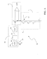
- Figure 3 schematically shows a sampling table used by the method for generating a reference current according to the invention;
- Figure 4 schematically shows a reference current generator using the method according to the invention;
- Figure 5 schematically shows a memory device comprising a reference current generator according to the invention;
- Figure 6 schematically shows an updating circuit associated to the generator of figure 4.
- The present invention relates to a method for generating a reference current for a reference line effective to be connected to a memory device, particularly of the Flash type.
- As seen with reference to the prior art, a reference current is obtained through a reference cell, advantageously of the Flash type, and it must be applied to a plurality of sense amplifiers associated to a reading architecture of the memory device. In order to simplify the invention description, elements being structurally and functionally identical to elements already described with reference to the prior art will be given the same numeral references.
- Contrary to what happens in known devices, wherein a current mirror is provided to transfer the reference cell current to sense
amplifiers 11 to be compared with a reading current of amatrix cell 12, the method according to the invention provides that the reference current REF is digitally coded by applying a convenient sampling thereof, as schematically shown in figure 3 showing, by way of example, a 4-bit Analog-to-Digital conversion with quantization on 16 possible levels for the reference current Irif considered in the range from 5uA to 27.5uA with a pitch of 1.5uA. - In particular, figure 3 shows a straight line A corresponding to the analogue values that can be taken by the reference current for memory cell reading operations and a stepped line B corresponding to the approximate reference current values obtained through a 4-bit Analog-to-Digital conversion.
- Advantageously in the method according to the invention, once the Analog-to-Digital conversion is performed, the reference cell current value is completely defined by a 4-bit digital signal REF_BIT[3:0] obtained from the Analog-to-Digital conversion.
- This digital signal REF_BIT[3:0] is then sent through a digital line to corresponding Digital-to-Analog conversion blocks to obtain the required reference current value REF1 to be applied to
sense amplifiers 11 to perform the reading operations of the memory cells connected thereto. - Advantageously according to the invention, this digital signal REF_BIT[3:0] obtained from the conversion of the analogue value REF of the reference current is free from noises and couplings, eliminating all stability problems of the analogue line REF_MIRROR and noise effect affecting prior art devices.
- Only Analog-to-Digital conversion operations A2D are added to obtain the digital signal REF_BIT[3:0] corresponding to the reference current analogue signal REF coding of the
reference cell 14, as well as Digital-to-Analog conversion operations D2A to reconstruct, starting from the coded value thereof, the digital signal REF_BIT[3:0], an analogue value REF1 of the reading reference current to be applied tosense amplifiers 11. - In other words, the method for generating a reference current for sense amplifiers connected to matrix cells of a memory device according to the invention comprises the following steps:
- generating a reading current analogue signal REF of a reference cell;
- converting this analogue signal REF into a reading current digital signal REF_BIT[3:0];
- sending this digital signal REF_BIT[3:0] to a memory device; and
- converting this digital signal REF_BIT[3:0] into a reference current
analogue signal REF1 to be applied to
sense amplifiers 11 comprised in this memory device. - At this moment,
sense amplifiers 11 can operate as in known memory devices, comparing this reference current analogue signal REF1 with the reading currents Icell of thematrix cells 12 connected thereto in order to determine the logic content. - It is worth noting that the reference current digital signal REF_BIT[3:0] is affected by the following errors:
- 1. Quantization error: caused by the Analog-to-Digital conversion process A2D;
- 2. Error caused by the unevenness between the Analog-to-Digital conversion process A2D and the inverse Digital-to-Analog conversion process D2A.
-
- However, it is worth noting that it is possible to set a priori the highest possible value of the quantization error. For example, with a discretization of the current analogue signal REF with pitches of 1.5uA (as shown for example in figure 3) a highest quantization error of 0,75uA is obtained.
- As for the error caused by unevenness, it is worth noting that the unevenness existing between conversion processes A2D and D2A can be actually compared with the unevenness of prior art devices wherein the reference current in
sense amplifiers 11 is reconstructed by using transistors being equal to the current mirror transistor performing the reference current transfer from thereference cell 13 to senseamplifiers 11. - The method according to the invention is thus extremely advantageous with respect to known methods since it is free from errors caused by couplings and parasitic capacitance, though being still subject to a slight quantization error having a highest value being known a priori.
- A reference current generator effective to implement the method according to the invention is schematically shown in figure 4, globally indicated with 40.
- The
generator 40 is connected between areference cell 14 effective to provide a reference current analogue signal REF and at least asense amplifier 11 effective to receive a reference current analogue signal REF1 to perform comparison operations with a reading current signal Icell passing through amatrix cell 12 connected thereto. - Advantageously according to the invention, the
generator 40 comprises, in cascade connection, an Analog-to-Digital conversion block 41 to perform the conversion of the analogue signal REF connected to a measure andlogic calculation block 42, connected in turn to adigital line 43 whereon the reference current conversion digital signal REF_BIT[3:0] is sent. - In particular, the measure and
logic calculation block 42 allows a periodical updating of the digital signal REF_BIT[3:0] to be implemented, as it will be explained hereafter. - The
digital line 43 is connected to a Digital-to-Analog conversion block 44 to perform the conversion of the digital signal REF_BIT[3:0] into the reference current analogue signal REF1 to be applied to thesense amplifiers 11. - As shown in figure 4, the
digital line 43 is free from the effects linked to the capacitive values 45 and to thecouplings 46 affecting the line REF_MIRROR used to transfer tosense amplifiers 11 the reference current in prior art devices. - Moreover, advantageously according to the invention, the
generator 40 provides a first 47 and second 48 dedicated lines connected to conversion blocks 41 and 44. - In particular, the first
dedicated line 47 provides conversion blocks 41 and 44 with a voltage reference, particularly a ground Gnd_ref, while the seconddedicated line 48 provides these blocks with a reference signal BGAP of the Band-Gap type obtained by means of a convenient Band-Gap generator 48A. - The use of these
dedicated lines noises 49 to be eliminated, as schematically shown in figure 4. - A
memory device 50 equipped with a single reference cell reading architecture is thus obtained, as schematically shown in figure 5. - Particularly, the
memory device 50 comprises amemory cell matrix 1 wherein amemory cell 12 is selected through abitline 2 and awordline 3. - Advantageously according to the invention, the
memory device 50 comprises a referencecurrent generator 40 connected between areference cell 14 and thesense amplifiers 11 and manufactured as previously indicated. - In an advantageous alternative embodiment of the method for generating a reference current according to the invention, it is possible to take into consideration temperature and voltage changes undergone by the reference cell and memory cells to avoid reading errors connected to these variations to occur. In this case, the method for generating the reference current according to the invention provides that conversion processes A2D and D2A are periodically performed, even when the memory device is in the stand-by condition.
- In particular, the updating frequency can be set at about one update per second, in order to pursue environmental temperature changes and also bias changes (for example battery voltage changes in mobile applications).
- Such an updating frequency is does not involve considerable increases in the memory device stand-by current but only negligible current increases caused by turning on a dedicated circuit performing the updating of conversion processes.
- Figure 6 schematically shows, globally indicated with 60, an updating circuit of the reference current digital signal REF_BIT[3:0].
- In particular, the updating
circuit 60 essentially comprises a state machine REF_UPDATE. - Advantageously according to the invention, the updating
circuit 60 is connected between acorresponding sense amplifier 11 of the memory device and theline 43 of the digital signal REF_BIT[3:0]. Thesense amplifiers 11 and the state machine REF_UPDATE as a whole form the measure andlogic calculation block 42 indicated in figure 4. - The
sense amplifier 11 is connected to the Digital-to-AnalogD2A conversion block 44 and to areference cell 14. - Advantageously according to the invention, the
conversion D2A block 44 is input a digital signal REF_BIT[3:0] coming from the updatingcircuit 60 and it provides a reconstructed current analogue circuit REF2. - The
reference cell 14 is periodically read with thesense amplifier 11, which compares the reference current obtained from thereference cell 14 with the current analogue signal REF2 obtained from theconversion D2A block 44. - The digital signal BIT[3:0] being input at the
conversion D2A block 44, in the considered example a 4-bit code, is generated by the state machine REF_UPDATE comprised in the updatingcircuit 60. In particular, this state machine REF_UPDATE increases or decreases the digital signal BIT[3:0] until a signal SOUT being output from thesense amplifier 11 does not commute. - In fact the commutation of the signal SOUT indicates that the reconstructed current analogue signal REF2 is equal to the current of the
reference cell 14. - At this point, the digital signal BIT[3:0] is sent on the
line 43 and allocated as value of the digital signal REF_BIT[3:0] to be sent to senseamplifiers 11. - Advantageously according to the invention, in correspondence with predetermined periodical ranges, the updating
circuit 60 turns thereference cell 14 on and it updates the value of the digital signal REF_BIT[3:0] on theline 43. - It is important to underline the fact that the Analog-to-Digital conversion A2D performed on the current of the reference cell 67 of the updating
circuit 60 is performed by using the same structures (sense amplifier 11 and Digital-to-Analog conversion block 44 globally indicated with 61 in figure 6) existing in the memory device, thus eliminating errors caused by different modes of performing a reference measurement. - In conclusion, the current generator implementing the method according to the invention is free from noises and couplings.
- Moreover, the digital signal corresponding to the reference current is always available (no setup time at the first reading after a stand-by) and it is periodically updated to take into consideration the temperature and supply voltage time changes.
- The updating frequency is such as not to considerably weigh on the stand-by consumption.
- The only error introduced is a quantization error linked to conversion processes A2D and D2A, whose highest value is however known a priori. It is worth noting that this quantization error can be reduced for example by increasing the number of bits coding the current analogue signal.
Claims (17)
- A method for generating a reference current (Iref) for sense amplifiers (11) connected to cells (12) of a memory matrix (1) comprising the steps of:characterised in that it further comprises the steps of:generating a first reference current analogue signal (REF) through a reference cell (14);performing an Analog-to-Digital conversion of said first analogue signal (REF) into a reference current digital signal (REF_BIT[3:0]);sending said digital signal (REF_BIT[3:0]) on a connection line (43) to said sense amplifiers (11); andperforming a Digital-to-Analog conversion of said digital signal (REF_BIT[3:0]) into a second reference current analogue signal (REF1) to be applied as reference current (Iref) to said sense amplifiers (11).
- A generation method according to claim 1, characterised in that it further provides a periodical updating step of said digital signal (REF_BIT[3:0]).
- A generation method according to claim 2, characterised in that said periodical updating step comprises the following steps of:turning said reference cell (14) on and reading a reference current through said sense amplifiers (11);generating a digital signal (BIT[3:0]) through a state machine (REF_UPDATE);performing a Digital-to-Analog conversion of said digital signal (BIT[3:0]) to generate a third reconstructed current analogue signal (REF2);comparing said reference current of said reference cell (14) with said third reconstructed current analogue signal (REF2);increasing and/or decreasing said digital signal (BIT[3:0]) until a commutation of a signal (SOUT) output from said sense amplifier (11); andsending said digital signal (BIT[3:0]) on said connection line (43) and allocation of said digital signal (BIT[3:0]) as value of said digital signal (REF_BIT[3:0]).
- A generation method according to claim 2, characterised in that said periodical updating step is performed at such a frequency as to pursue environmental temperature and bias changes undergone by said cells (12) of said memory matrix (1).
- A generation method according to claim 4, characterised in that said periodical updating step is performed at a frequency of an update per second.
- A generation method according to claim 1, characterised in that said Analog-to-Digital conversion step comprises a 4-bit conversion with quantization on 16 levels.
- A generator (40) of a reference current (Iref) for sense amplifiers (11) connected to cells (12) of a memory matrix (1), said generator (4) being connected to a reference cell (14) effective to provide a reference current analogue signal (REF) and characterised in that it comprises:an Analog-to-Digital conversion block (41) inserted between said reference cell (14) and a connection line (43) and effective to perform a conversion of said reference current analogue signal (REF) in a digital conversion signal (REF_BIT[3:0]) of the reference current sent on said one connection line (43); anda Digital-to-Analog conversion block (44) inserted between said connection line (43) and said sense amplifiers (11) and effective to perform a conversion of said digital signal (REF_BIT[3:0]) received from said connection line (43) into a reference current analogue signal (REF1) to be applied to said sense amplifiers (11).
- A generator according to claim 7, characterised in that it comprises at least a first dedicated line (47) connected to said Analog-to-Digital (41) and Digital-to-Analog (44) conversion blocks and effective to provide a voltage reference (Gnd_ref).
- A generator according to claim 7, characterised in that it comprises at least a second dedicated line (48) connected to said Analog-to-Digital (41) and Digital-to-Analog (44) conversion blocks and effective to provide a Band-Gap reference signal (BGAP).
- A generator according to claim 9, characterised in that it comprises at least a Band-Gap generator (48A) connected to said second dedicated line (48).
- A generator according to claim 7, characterised in that it further comprises an updating circuit (60) of said reference current digital signal (REF_BIT[3:0]) connected between said sense amplifiers (11) and said connection line (43), said updating circuit (60) essentially comprising a state machine (REF_UPDATE) effective to generate a digital signal BIT[3:0] applied to said Digital-to-Analog conversion block (44), effective in turn to provide a reconstructed current analogue signal (REF2).
- A generator according to claim 11, characterised in that said updating circuit (60) causes a turn on of said reference cell (14), a reading of a corresponding reference current by said sense amplifiers (11) and a comparison of said reference current with said reconstructed current analogue signal (REF2) and in that said state machine (REF_UPDATE) increases and/or decreases said digital signal (BIT[3:0]) until a commutation of a signal (SOUT) output from said sense amplifiers (11) is performed.
- A generator according to claim 12, characterised in that said state machine (REF_UPDATE) sends, in correspondence with said commutation of a signal (SOUT) output from said sense amplifiers (11), said digital signal (BIT[3:0]) on said connection line (43), allocating it as updated value of said digital signal (REF_BIT[3:0]).
- A generator according to claim 12, characterised in that said updating circuit (60) turns said reference cell (14) on and it periodically updates said value of said digital signal (REF_BIT[3:0]) with predetermined frequency.
- A generator according to claim 14, characterised in that said updating circuit (60) provides such a frequency as to pursue environmental temperature and bias changes undergone by said cells (12) of said memory matrix (1).
- A generator according to claim 14, characterised in that said updating circuit (60) provides a frequency of an update per second.
- A memory device of the type comprising a single reference cell reading architecture characterised in that it comprises a generator according to one of claims 7 to 16.
Priority Applications (3)
| Application Number | Priority Date | Filing Date | Title |
|---|---|---|---|
| EP03425353A EP1484764B1 (en) | 2003-06-04 | 2003-06-04 | Method for generating a reference current for sense amplifiers connected to cells of a memory matrix, particularly in big-sized flash memories, and corresponding generator |
| DE60307606T DE60307606D1 (en) | 2003-06-04 | 2003-06-04 | Method for generating reference current signals for sense amplifiers for semiconductor memory cells and generator thereto |
| US10/861,340 US7006025B2 (en) | 2003-06-04 | 2004-06-04 | Method for generating a reference current for sense amplifiers and corresponding generator |
Applications Claiming Priority (1)
| Application Number | Priority Date | Filing Date | Title |
|---|---|---|---|
| EP03425353A EP1484764B1 (en) | 2003-06-04 | 2003-06-04 | Method for generating a reference current for sense amplifiers connected to cells of a memory matrix, particularly in big-sized flash memories, and corresponding generator |
Publications (2)
| Publication Number | Publication Date |
|---|---|
| EP1484764A1 true EP1484764A1 (en) | 2004-12-08 |
| EP1484764B1 EP1484764B1 (en) | 2006-08-16 |
Family
ID=33155299
Family Applications (1)
| Application Number | Title | Priority Date | Filing Date |
|---|---|---|---|
| EP03425353A Expired - Lifetime EP1484764B1 (en) | 2003-06-04 | 2003-06-04 | Method for generating a reference current for sense amplifiers connected to cells of a memory matrix, particularly in big-sized flash memories, and corresponding generator |
Country Status (3)
| Country | Link |
|---|---|
| US (1) | US7006025B2 (en) |
| EP (1) | EP1484764B1 (en) |
| DE (1) | DE60307606D1 (en) |
Cited By (2)
| Publication number | Priority date | Publication date | Assignee | Title |
|---|---|---|---|---|
| JP2012169032A (en) * | 2011-02-11 | 2012-09-06 | Freescale Semiconductor Inc | Digital method and apparatus for obtaining i-v curves of non-volatile memory bit cells |
| WO2016007372A1 (en) * | 2014-07-07 | 2016-01-14 | Sandisk Technologies Inc. | Selective sense amplifier enablement |
Families Citing this family (2)
| Publication number | Priority date | Publication date | Assignee | Title |
|---|---|---|---|---|
| CN103827972A (en) | 2011-08-26 | 2014-05-28 | 惠普发展公司,有限责任合伙企业 | Circuit and method for reading resistive switching devices in an array |
| JP2016207243A (en) * | 2015-04-24 | 2016-12-08 | 株式会社デンソー | Semiconductor memory device |
Citations (2)
| Publication number | Priority date | Publication date | Assignee | Title |
|---|---|---|---|---|
| US6141261A (en) * | 1999-12-31 | 2000-10-31 | Patti; Robert | DRAM that stores multiple bits per storage cell |
| US20010003507A1 (en) * | 1999-12-08 | 2001-06-14 | Matsushita Electric Industrial Co., Ltd. | Nonvolatile semiconductor memory device |
Family Cites Families (4)
| Publication number | Priority date | Publication date | Assignee | Title |
|---|---|---|---|---|
| US5880988A (en) * | 1997-07-11 | 1999-03-09 | International Business Machines Corporation | Reference potential for sensing data in electronic storage element |
| US6314014B1 (en) * | 1999-12-16 | 2001-11-06 | Ovonyx, Inc. | Programmable resistance memory arrays with reference cells |
| US6590804B1 (en) * | 2002-07-16 | 2003-07-08 | Hewlett-Packard Development Company, L.P. | Adjustable current mode differential amplifier |
| US6674679B1 (en) * | 2002-10-01 | 2004-01-06 | Hewlett-Packard Development Company, L.P. | Adjustable current mode differential amplifier for multiple bias point sensing of MRAM having equi-potential isolation |
-
2003
- 2003-06-04 EP EP03425353A patent/EP1484764B1/en not_active Expired - Lifetime
- 2003-06-04 DE DE60307606T patent/DE60307606D1/en not_active Expired - Lifetime
-
2004
- 2004-06-04 US US10/861,340 patent/US7006025B2/en not_active Expired - Fee Related
Patent Citations (2)
| Publication number | Priority date | Publication date | Assignee | Title |
|---|---|---|---|---|
| US20010003507A1 (en) * | 1999-12-08 | 2001-06-14 | Matsushita Electric Industrial Co., Ltd. | Nonvolatile semiconductor memory device |
| US6141261A (en) * | 1999-12-31 | 2000-10-31 | Patti; Robert | DRAM that stores multiple bits per storage cell |
Cited By (2)
| Publication number | Priority date | Publication date | Assignee | Title |
|---|---|---|---|---|
| JP2012169032A (en) * | 2011-02-11 | 2012-09-06 | Freescale Semiconductor Inc | Digital method and apparatus for obtaining i-v curves of non-volatile memory bit cells |
| WO2016007372A1 (en) * | 2014-07-07 | 2016-01-14 | Sandisk Technologies Inc. | Selective sense amplifier enablement |
Also Published As
| Publication number | Publication date |
|---|---|
| DE60307606D1 (en) | 2006-09-28 |
| US7006025B2 (en) | 2006-02-28 |
| US20050040977A1 (en) | 2005-02-24 |
| EP1484764B1 (en) | 2006-08-16 |
Similar Documents
| Publication | Publication Date | Title |
|---|---|---|
| US6324094B1 (en) | Apparatus for reading state of multistate non-volatile memory cells | |
| US5790453A (en) | Apparatus and method for reading state of multistate non-volatile memory cells | |
| JP4215803B2 (en) | Memory with uniform read and verify thresholds | |
| EP1023731B1 (en) | Sense amplifier for flash memories | |
| US8488398B2 (en) | Threshold voltage digitizer for array of programmable threshold transistors | |
| US7366021B2 (en) | Method and apparatus for sensing flash memory using delta sigma modulation | |
| US6424570B1 (en) | Modulated charge pump with uses an analog to digital converter to compensate for supply voltage variations | |
| EP1050052B1 (en) | Non-volatile memory with improved sensing and method therefor | |
| US7636263B2 (en) | Semiconductor memory having function to determine semiconductor low current | |
| US6655758B2 (en) | Method for storing data in a nonvolatile memory | |
| US20040105311A1 (en) | Non-volatile memory with improved sensing and method therefor | |
| JPH10501362A (en) | Dynamic memory from single bit per cell to multiple bits per cell | |
| KR20040043165A (en) | A voltage boost circuit using supply voltage detection to compensate for supply voltage variations in read mode voltages | |
| US4974207A (en) | Semiconductor memory device | |
| EP1484764B1 (en) | Method for generating a reference current for sense amplifiers connected to cells of a memory matrix, particularly in big-sized flash memories, and corresponding generator | |
| KR100309299B1 (en) | Semiconductor memory device which can be set one from multiple threshold value | |
| US6373767B1 (en) | Memory that stores multiple bits per storage cell | |
| US7453727B2 (en) | Nonvolatile semiconductor memory and method for setting replacement information in nonvolatile semiconductor memory | |
| US12300342B2 (en) | System and method for testing a non-volatile memory | |
| US6707725B2 (en) | Reference voltage generation circuit for semiconductor memory device, memory reading circuit including same, and electronic information device including the same | |
| US7596025B2 (en) | Semiconductor memory device and method of controlling semiconductor memory device | |
| WO1998008226A1 (en) | A flash memory device having a page mode of operation | |
| CN114664355B (en) | Reference current generating module and reference current setting method of nonvolatile memory | |
| KR20230096796A (en) | Semiconductor device | |
| JPH02123597A (en) | Nonvolatile memory |
Legal Events
| Date | Code | Title | Description |
|---|---|---|---|
| PUAI | Public reference made under article 153(3) epc to a published international application that has entered the european phase |
Free format text: ORIGINAL CODE: 0009012 |
|
| AK | Designated contracting states |
Kind code of ref document: A1 Designated state(s): AT BE BG CH CY CZ DE DK EE ES FI FR GB GR HU IE IT LI LU MC NL PT RO SE SI SK TR |
|
| AX | Request for extension of the european patent |
Extension state: AL LT LV MK |
|
| 17P | Request for examination filed |
Effective date: 20050601 |
|
| AKX | Designation fees paid |
Designated state(s): DE FR GB IT |
|
| GRAP | Despatch of communication of intention to grant a patent |
Free format text: ORIGINAL CODE: EPIDOSNIGR1 |
|
| GRAS | Grant fee paid |
Free format text: ORIGINAL CODE: EPIDOSNIGR3 |
|
| GRAA | (expected) grant |
Free format text: ORIGINAL CODE: 0009210 |
|
| AK | Designated contracting states |
Kind code of ref document: B1 Designated state(s): DE FR GB IT |
|
| PG25 | Lapsed in a contracting state [announced via postgrant information from national office to epo] |
Ref country code: IT Free format text: LAPSE BECAUSE OF FAILURE TO SUBMIT A TRANSLATION OF THE DESCRIPTION OR TO PAY THE FEE WITHIN THE PRESCRIBED TIME-LIMIT;WARNING: LAPSES OF ITALIAN PATENTS WITH EFFECTIVE DATE BEFORE 2007 MAY HAVE OCCURRED AT ANY TIME BEFORE 2007. THE CORRECT EFFECTIVE DATE MAY BE DIFFERENT FROM THE ONE RECORDED. Effective date: 20060816 |
|
| REG | Reference to a national code |
Ref country code: GB Ref legal event code: FG4D |
|
| REF | Corresponds to: |
Ref document number: 60307606 Country of ref document: DE Date of ref document: 20060928 Kind code of ref document: P |
|
| PG25 | Lapsed in a contracting state [announced via postgrant information from national office to epo] |
Ref country code: DE Free format text: LAPSE BECAUSE OF FAILURE TO SUBMIT A TRANSLATION OF THE DESCRIPTION OR TO PAY THE FEE WITHIN THE PRESCRIBED TIME-LIMIT Effective date: 20061117 |
|
| ET | Fr: translation filed | ||
| PLBE | No opposition filed within time limit |
Free format text: ORIGINAL CODE: 0009261 |
|
| STAA | Information on the status of an ep patent application or granted ep patent |
Free format text: STATUS: NO OPPOSITION FILED WITHIN TIME LIMIT |
|
| 26N | No opposition filed |
Effective date: 20070518 |
|
| PGFP | Annual fee paid to national office [announced via postgrant information from national office to epo] |
Ref country code: IT Payment date: 20080614 Year of fee payment: 6 |
|
| PGFP | Annual fee paid to national office [announced via postgrant information from national office to epo] |
Ref country code: FR Payment date: 20080630 Year of fee payment: 6 |
|
| PGFP | Annual fee paid to national office [announced via postgrant information from national office to epo] |
Ref country code: GB Payment date: 20080527 Year of fee payment: 6 |
|
| GBPC | Gb: european patent ceased through non-payment of renewal fee |
Effective date: 20090604 |
|
| REG | Reference to a national code |
Ref country code: FR Ref legal event code: ST Effective date: 20100226 |
|
| PG25 | Lapsed in a contracting state [announced via postgrant information from national office to epo] |
Ref country code: FR Free format text: LAPSE BECAUSE OF NON-PAYMENT OF DUE FEES Effective date: 20090630 |
|
| PG25 | Lapsed in a contracting state [announced via postgrant information from national office to epo] |
Ref country code: GB Free format text: LAPSE BECAUSE OF NON-PAYMENT OF DUE FEES Effective date: 20090604 |
|
| PG25 | Lapsed in a contracting state [announced via postgrant information from national office to epo] |
Ref country code: IT Free format text: LAPSE BECAUSE OF NON-PAYMENT OF DUE FEES Effective date: 20090604 |