EP1484631A1 - Integrierte Optoelektronische Vorrichtung mit einem Elektroabsorptionsmodulator und dessen elektronisches Steuerelement - Google Patents
Integrierte Optoelektronische Vorrichtung mit einem Elektroabsorptionsmodulator und dessen elektronisches Steuerelement Download PDFInfo
- Publication number
- EP1484631A1 EP1484631A1 EP04291368A EP04291368A EP1484631A1 EP 1484631 A1 EP1484631 A1 EP 1484631A1 EP 04291368 A EP04291368 A EP 04291368A EP 04291368 A EP04291368 A EP 04291368A EP 1484631 A1 EP1484631 A1 EP 1484631A1
- Authority
- EP
- European Patent Office
- Prior art keywords
- sections
- optoelectronic device
- modulator
- modulation
- optical
- Prior art date
- Legal status (The legal status is an assumption and is not a legal conclusion. Google has not performed a legal analysis and makes no representation as to the accuracy of the status listed.)
- Withdrawn
Links
Images
Classifications
-
- G—PHYSICS
- G02—OPTICS
- G02F—OPTICAL DEVICES OR ARRANGEMENTS FOR THE CONTROL OF LIGHT BY MODIFICATION OF THE OPTICAL PROPERTIES OF THE MEDIA OF THE ELEMENTS INVOLVED THEREIN; NON-LINEAR OPTICS; FREQUENCY-CHANGING OF LIGHT; OPTICAL LOGIC ELEMENTS; OPTICAL ANALOGUE/DIGITAL CONVERTERS
- G02F1/00—Devices or arrangements for the control of the intensity, colour, phase, polarisation or direction of light arriving from an independent light source, e.g. switching, gating or modulating; Non-linear optics
- G02F1/01—Devices or arrangements for the control of the intensity, colour, phase, polarisation or direction of light arriving from an independent light source, e.g. switching, gating or modulating; Non-linear optics for the control of the intensity, phase, polarisation or colour
- G02F1/015—Devices or arrangements for the control of the intensity, colour, phase, polarisation or direction of light arriving from an independent light source, e.g. switching, gating or modulating; Non-linear optics for the control of the intensity, phase, polarisation or colour based on semiconductor elements with at least one potential jump barrier, e.g. PN, PIN junction
- G02F1/017—Structures with periodic or quasi periodic potential variation, e.g. superlattices, quantum wells
- G02F1/01708—Structures with periodic or quasi periodic potential variation, e.g. superlattices, quantum wells in an optical wavequide structure
-
- B—PERFORMING OPERATIONS; TRANSPORTING
- B82—NANOTECHNOLOGY
- B82Y—SPECIFIC USES OR APPLICATIONS OF NANOSTRUCTURES; MEASUREMENT OR ANALYSIS OF NANOSTRUCTURES; MANUFACTURE OR TREATMENT OF NANOSTRUCTURES
- B82Y20/00—Nanooptics, e.g. quantum optics or photonic crystals
-
- G—PHYSICS
- G02—OPTICS
- G02F—OPTICAL DEVICES OR ARRANGEMENTS FOR THE CONTROL OF LIGHT BY MODIFICATION OF THE OPTICAL PROPERTIES OF THE MEDIA OF THE ELEMENTS INVOLVED THEREIN; NON-LINEAR OPTICS; FREQUENCY-CHANGING OF LIGHT; OPTICAL LOGIC ELEMENTS; OPTICAL ANALOGUE/DIGITAL CONVERTERS
- G02F1/00—Devices or arrangements for the control of the intensity, colour, phase, polarisation or direction of light arriving from an independent light source, e.g. switching, gating or modulating; Non-linear optics
- G02F1/01—Devices or arrangements for the control of the intensity, colour, phase, polarisation or direction of light arriving from an independent light source, e.g. switching, gating or modulating; Non-linear optics for the control of the intensity, phase, polarisation or colour
- G02F1/0121—Operation of devices; Circuit arrangements, not otherwise provided for in this subclass
-
- G—PHYSICS
- G02—OPTICS
- G02F—OPTICAL DEVICES OR ARRANGEMENTS FOR THE CONTROL OF LIGHT BY MODIFICATION OF THE OPTICAL PROPERTIES OF THE MEDIA OF THE ELEMENTS INVOLVED THEREIN; NON-LINEAR OPTICS; FREQUENCY-CHANGING OF LIGHT; OPTICAL LOGIC ELEMENTS; OPTICAL ANALOGUE/DIGITAL CONVERTERS
- G02F1/00—Devices or arrangements for the control of the intensity, colour, phase, polarisation or direction of light arriving from an independent light source, e.g. switching, gating or modulating; Non-linear optics
- G02F1/01—Devices or arrangements for the control of the intensity, colour, phase, polarisation or direction of light arriving from an independent light source, e.g. switching, gating or modulating; Non-linear optics for the control of the intensity, phase, polarisation or colour
- G02F1/015—Devices or arrangements for the control of the intensity, colour, phase, polarisation or direction of light arriving from an independent light source, e.g. switching, gating or modulating; Non-linear optics for the control of the intensity, phase, polarisation or colour based on semiconductor elements with at least one potential jump barrier, e.g. PN, PIN junction
- G02F1/0155—Devices or arrangements for the control of the intensity, colour, phase, polarisation or direction of light arriving from an independent light source, e.g. switching, gating or modulating; Non-linear optics for the control of the intensity, phase, polarisation or colour based on semiconductor elements with at least one potential jump barrier, e.g. PN, PIN junction modulating the optical absorption
Definitions
- the invention relates to the field of high-speed data transmission.
- fiber optic throughput and more particularly relates to a device integrated optoelectronics with a suitable electroabsorption modulator providing a modulated optical data carrier output signal, and a electronic control element capable of controlling said modulator.
- electroabsorption modulators discrete modulators and those with traveling waves.
- R s the series resistance of the modulator, R L ⁇ 50 ⁇ , the impedance of the control source, C m the capacity of the modulator.
- a discrete modulator operates correctly at 40 GHz, with a length of around 100 ⁇ m, a capacitance C m of around 70 fF and a series resistance R s of around 5 ⁇ .
- the cut-off frequency is greater the longer the length of the electrode is weak. To operate at high speed, for example at 80 or 160 Gbit / s, it would therefore be necessary to drastically reduce this length, with intrinsic zone thickness and guide width given. However, the reduction in length is accompanied by a decrease in efficiency optics translated by a low extinction rate, and requires voltages of very high command required, interaction distance optical / electrical is no longer sufficient.
- the traveling wave electroabsorption modulator (TWEAM for "traveling waves electrabsorption modulator” in English) is characterized by its electrode distributed so that there is double propagation: the propagation of guided light and the propagation of an electric wave. During their copropagation, there is transfer of the modulation energy of the electrical signal to optical signal.
- TWEAM traveling wave electroabsorption modulator
- Progressive wave electro-absorption modulators are in technology based on lithium niobiate or more recently, such as discrete modulators, in technology based on semiconductor materials III-V, of the InGaAsP type. These semiconductor materials have a voltage of control, therefore lower consumption and the modulators produced are less bulky.
- the traveling wave modulators theoretically allow to overcome of the problem of limiting electric bandwidth.
- the losses of the electric wave during its propagation the length of the electrode are important and impose a length limit for a fixed bandwidth.
- the characteristic impedance of the line of modulator propagation is generally too low compared to that of the control transistor, which limits the electrical power transmitted to the modulator.
- the voltage gain is too low at high frequency.
- Discrete and wave electro-absorption modulators progressive are therefore not efficient beyond 40 GHz.
- the object of the invention is to provide an optoelectronic device integrated with a space-saving electro-absorption modulator consumer, operating at high speed and producing one or more signals modulated optics having an extinction rate and an optical power satisfactory.
- the modulator electroabsorption according to the invention is distributed as is the amplification electric is distributed: each modulation section, electroabsorption, participates in the generation of a modulated optical signal which, at output, presents an extinction rate (in dB) corresponding to the sum of the extinction rates sections.
- the electronic control element according to the invention is chosen fast and has a high total voltage gain.
- This element is capable of supplying control signals, for example voltages of control, from peak to peak level sufficient and adjusted for each section modulation.
- the means of distributed electrical amplification are such as the control signal from the most upstream modulation section, which receives a continuous optical input signal, is of lower intensity than the signal control of the most downstream modulation section.
- At least one of said modulation sections receiving a modulated optical input signal some of said sections are phase adjustment means so as to phase, at the level at least said section, the control signal with said optical signal modulated input, to avoid data jamming.
- an optical amplifier preferably solid-state, of so as to compensate for optical losses.
- the modulation sections can each be traveling wave.
- the means of distributed electrical amplification may include a plurality of transistors with high electron mobility and preferably heterojunction bipolar transistors or field effect transistors such as' HEMT (HEMT in English for high electron mobility transistor). Said transistors are connected to the same other propagation line which is capable of carrying a modulated electrical signal, for example from a time multiplexer.
- the modulation sections can be aligned and the line of electrical propagation for control signals may have a form niche type and preferably include at the entry and exit means of impedance matching.
- the impedance of the electrical propagation line for control signals can thus be easily adjusted and reduced if necessary.
- the optoelectronic device may include a source of at least less a continuous optical signal, arranged upstream of said modulator by relative to the direction of optical propagation, such as a laser source, as well as a optical waveguide disposed downstream of said modulator with respect to the direction optical propagation.
- a source of at least less a continuous optical signal arranged upstream of said modulator by relative to the direction of optical propagation, such as a laser source, as well as a optical waveguide disposed downstream of said modulator with respect to the direction optical propagation.
- the device optoelectronics is monolithic and preferably produced on a substrate with indium phosphide base for great compactness.
- the modulator electroabsorption is carried out on a substrate based on indium phosphide, while the electronic control element is hybrid and is made in part on a separate substrate based on gallium arsenide or phosphide indium. And some of the sections, called interconnections, are chosen from gold ribbons, gold wires and other flexible conductive elements.
- the invention naturally applies to any transmission system incorporating the integrated optoelectronic device as defined previously.
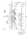
- FIG. 1 a top view which is not to the scale of a integrated optoelectronic device 100, in a preferred embodiment of the invention
- the optoelectronic device 100 is an integrated source of minus a high speed modulated optical signal insertable into a transmission (not shown) for example containing an optical fiber of transmission.
- the device 100 is preferably monolithic and produced on a substrate 111 of indium phosphide InP.
- the device 100 is designed to operate at high speed for example at 160 GHz, i.e. a modulation wavelength of 300 ⁇ m.
- each electrode 1, 2, 3 is distributed and chosen length less than or equal to 300 ⁇ m to form a line of transmission.
- the set of distributed electrical amplification means is formed of three electrical amplifiers 22, 23, 24, each consisting of a transistor with high electron mobility, for example preferably bipolar heterojunction.
- Each transmitter is connected to an earth M22, M23, M24.
- each of the transistors 22 to 24 heterojunction bipolar and followed by a second bipolar transistor with heterojunction mounted in 'cascode' to provide a control signal for best quality.
- transistors 22 to 24 may as well have the effect of field.
- Transistors 22 to 24 are connected by their collector to separate points A; B; C of the first line of electrical 21 which corresponds thus to an exit line.
- This first electrical line 21, substantially shaped in niche in particular for a gain in compactness, comprises a plurality of sections, for example sixteen, between an adaptation input impedance of line ZL2 connected to a ground M2 and an adaptation output impedance of line ZL3 connected to ground M3.
- These impedances ZL2, ZL3 can be distinct from 50 ⁇ .
- the impedances are adjusted by the choice of the width, by example equal to 20 ⁇ m, and of the length and are for example inductors worth approximately 100 nH / m.
- the bases of the transistors 22 to 24 are further connected by links LK1 to LK3 at separate points A ', B', C 'of the second line of electric 25 which thus corresponds to an input line.
- the second electric line 25 is thus divided into four sections referenced by their impedances Za to Zd each being adjusted by the choice width, preferably equal to 10 ⁇ m, and length.
- the impedances Za to Zd correspond for example to inductances of around 250 nH / m.
- This second electrical line 25 is itself connected at the input to a single output branch 6 5 of a time electrical multiplexer 6 with four input branches 6 1 to 6 4 and at the output to a load resistor ZL1, for example equal to 50 ⁇ or less, connected to ground M1.
- Transistors 22 to 24 are supplied with voltage Va, Vb, Vc from of the second power line 25 and provide electrical signals amplified modules which are control currents which generate control voltages V1, V2, V3 propagating in the first line electric 21.
- the voltage of command V2 is chosen according to the losses as well as the voltage of command V3 at the input of the third modulation section 13.
- a continuous optical signal S i of power for example equal to approximately 1 W, is generated by the laser source 4 and amplified by the amplifier 31.
- this signal S i is modulated at a rate of 160 Gbit / s by the control voltage V1 applied to electrode 1.
- the extinction rate is around 6 dB.
- the modulated optical signal S mod is then amplified by the amplifier 32 and injected into the second modulation section 12.
- the modulation is reinforced by the control voltage V2 in phase with this modulated optical signal, thanks to the section 21 a.
- the extinction rate is around 13 dB.
- a high speed modulated signal S f is obtained at the output of the guide 5 with a power of the order of at least 0 dBm and an extinction rate equal to 13 dB minimum.
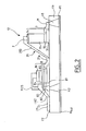
- Figure 2 schematically shows a partial view, in section lateral along axis II, which is not to scale, of the optoelectronic device integrated 100.
- the cut is made at the second section of modulation 12, as an example.
- the modulation section 12 has a vertical structure 7 which is a stack of epitaxial layers produced on the so-called upper face F1 of substrate 111.
- the electrode section 2 by example a titanium, platinum and gold multilayer 2 ⁇ m thick.
- the first line of electrical 25 for example a multilayer titanium, platinum and gold 2 ⁇ m thick is connected by the LK2 link to the base of transistor 23.
- the link LK2 and the interconnection sections 213, are also a titanium multilayer, platinum and gold formed for example on an insulating material such as polyimide (not shown).
- the electronic control element 20 is hybrid for ease of production and is partly produced on a separate substrate based on arsenide of gallium or gallium or indium phosphide.
- the sections interconnections 211 to 216 are then chosen from gold-based wires, gold-based tapes and other flexible conductive elements such as a ribbon polyimide coated with copper.
- Continuous source 4 electroabsorption modulator 30, series 30 of four optical amplifiers and the output optical guide 5 are manufactured on the substrate 111 in indium phosphide InP.
- modulation sections may as well be greater together. Their length is adjusted according to the desired performance.
Applications Claiming Priority (2)
| Application Number | Priority Date | Filing Date | Title |
|---|---|---|---|
| FR0306662 | 2003-06-03 | ||
| FR0306662A FR2855883B1 (fr) | 2003-06-03 | 2003-06-03 | Dispositif optoelectronique integre comportant un modulateur a electroabsorption et un element electronique de commande du modulateur |
Publications (1)
| Publication Number | Publication Date |
|---|---|
| EP1484631A1 true EP1484631A1 (de) | 2004-12-08 |
Family
ID=33155642
Family Applications (1)
| Application Number | Title | Priority Date | Filing Date |
|---|---|---|---|
| EP04291368A Withdrawn EP1484631A1 (de) | 2003-06-03 | 2004-06-01 | Integrierte Optoelektronische Vorrichtung mit einem Elektroabsorptionsmodulator und dessen elektronisches Steuerelement |
Country Status (3)
| Country | Link |
|---|---|
| US (1) | US20040246557A1 (de) |
| EP (1) | EP1484631A1 (de) |
| FR (1) | FR2855883B1 (de) |
Cited By (1)
| Publication number | Priority date | Publication date | Assignee | Title |
|---|---|---|---|---|
| CN104768454A (zh) * | 2012-11-08 | 2015-07-08 | 皇家飞利浦有限公司 | 光学探头系统 |
Families Citing this family (12)
| Publication number | Priority date | Publication date | Assignee | Title |
|---|---|---|---|---|
| GB0206226D0 (en) * | 2002-03-16 | 2002-05-01 | Intense Photonics Ltd | Electro-absorption modulator with broad optical bandwidth |
| US7515775B1 (en) | 2003-08-15 | 2009-04-07 | Luxtera, Inc. | Distributed amplifier optical modulator |
| US7039258B2 (en) * | 2003-08-15 | 2006-05-02 | Luxtera, Inc. | Distributed amplifier optical modulators |
| US10928659B2 (en) | 2014-02-24 | 2021-02-23 | Rockley Photonics Limited | Optoelectronic device |
| US10921616B2 (en) | 2016-11-23 | 2021-02-16 | Rockley Photonics Limited | Optoelectronic device |
| US11150494B2 (en) | 2015-03-05 | 2021-10-19 | Rockley Photonics Limited | Waveguide modulator structures |
| GB2546279B (en) | 2016-01-12 | 2019-08-21 | Phoelex Ltd | An optical apparatus |
| US11101256B2 (en) | 2016-11-23 | 2021-08-24 | Rockley Photonics Limited | Optical modulators |
| US10135542B2 (en) * | 2016-12-15 | 2018-11-20 | Rockley Photonics Limited | Optical modulators |
| US11105975B2 (en) | 2016-12-02 | 2021-08-31 | Rockley Photonics Limited | Waveguide optoelectronic device |
| WO2018100172A1 (en) | 2016-12-02 | 2018-06-07 | Rockley Photonics Limited | Waveguide device and method of doping a waveguide device |
| CN109638638B (zh) * | 2017-10-05 | 2023-06-13 | 住友电工光电子器件创新株式会社 | 光学模块 |
Citations (3)
| Publication number | Priority date | Publication date | Assignee | Title |
|---|---|---|---|---|
| EP0741316A1 (de) * | 1992-02-03 | 1996-11-06 | Kokusai Denshin Denwa Kabushiki Kaisha | Optischer Impulsgeber |
| WO2003013031A1 (en) * | 2001-08-01 | 2003-02-13 | Optillion Ab | Modulator transmitter for high-speed fiberoptic communications |
| US6529646B1 (en) * | 1999-02-23 | 2003-03-04 | Marconi Caswell Limited | Optical modulator |
Family Cites Families (8)
| Publication number | Priority date | Publication date | Assignee | Title |
|---|---|---|---|---|
| US5046155A (en) * | 1990-04-06 | 1991-09-03 | Wisconsin Alumni Research Foundation | Highly directive, broadband, bidirectional distributed amplifier |
| US5355422A (en) * | 1992-11-09 | 1994-10-11 | Honeywell Inc. | Broadband optical modulator |
| FR2711277B1 (fr) * | 1993-10-14 | 1995-11-10 | Alcatel Mobile Comm France | Antenne du type pour dispositif radio portable, procédé de fabrication d'une telle antenne et dispositif radio portable comportant une telle antenne. |
| US20040165246A1 (en) * | 1999-11-03 | 2004-08-26 | Carlson Steven Allen | Electro-optic modulators |
| US6525857B1 (en) * | 2000-03-07 | 2003-02-25 | Opvista, Inc. | Method and apparatus for interleaved optical single sideband modulation |
| WO2003032547A2 (en) * | 2001-10-09 | 2003-04-17 | Infinera Corporation | Transmitter photonic integrated circuit |
| US6990256B2 (en) * | 2002-06-20 | 2006-01-24 | Triquint Technology Holding Co. | Segmented modulator for high-speed opto-electronics |
| US7039258B2 (en) * | 2003-08-15 | 2006-05-02 | Luxtera, Inc. | Distributed amplifier optical modulators |
-
2003
- 2003-06-03 FR FR0306662A patent/FR2855883B1/fr not_active Expired - Fee Related
-
2004
- 2004-05-28 US US10/855,332 patent/US20040246557A1/en not_active Abandoned
- 2004-06-01 EP EP04291368A patent/EP1484631A1/de not_active Withdrawn
Patent Citations (3)
| Publication number | Priority date | Publication date | Assignee | Title |
|---|---|---|---|---|
| EP0741316A1 (de) * | 1992-02-03 | 1996-11-06 | Kokusai Denshin Denwa Kabushiki Kaisha | Optischer Impulsgeber |
| US6529646B1 (en) * | 1999-02-23 | 2003-03-04 | Marconi Caswell Limited | Optical modulator |
| WO2003013031A1 (en) * | 2001-08-01 | 2003-02-13 | Optillion Ab | Modulator transmitter for high-speed fiberoptic communications |
Non-Patent Citations (1)
| Title |
|---|
| LIAO H H ET AL: "DESIGN OF MILLIMETER WAVE OPTICAL MODULATORS WITH MONOLITHICALLY INTEGRATED NARROW BAND IMPEDANCE MATCHING CIRCUITS FOR 1.3MUM PHOTONIC LINKS", PROCEEDINGS OF THE SPIE, SPIE, BELLINGHAM, VA, US, vol. 2844, August 1996 (1996-08-01), pages 97 - 107, XP000889754, ISSN: 0277-786X * |
Cited By (1)
| Publication number | Priority date | Publication date | Assignee | Title |
|---|---|---|---|---|
| CN104768454A (zh) * | 2012-11-08 | 2015-07-08 | 皇家飞利浦有限公司 | 光学探头系统 |
Also Published As
| Publication number | Publication date |
|---|---|
| FR2855883A1 (fr) | 2004-12-10 |
| FR2855883B1 (fr) | 2005-08-26 |
| US20040246557A1 (en) | 2004-12-09 |
Similar Documents
| Publication | Publication Date | Title |
|---|---|---|
| EP1484631A1 (de) | Integrierte Optoelektronische Vorrichtung mit einem Elektroabsorptionsmodulator und dessen elektronisches Steuerelement | |
| EP0017571A1 (de) | Lichtintensitätsmodulator in integrierter Optik und integrierte optische Schaltung mit einem solchen Modulator | |
| FR2949872A1 (fr) | Dispositif de modulation electro-optique | |
| FR2756938A1 (fr) | Dispositif, notamment a semiconducteur, pour le traitement de deux ondes, notamment lumineuses | |
| FR2753285A1 (fr) | Amplificateur optique a semi conducteur | |
| FR2762105A1 (fr) | Convertisseur de longueur d'onde de signaux optiques binaires | |
| EP0562925B1 (de) | Wellenleiter-Photoempfänger aus Halbleitermaterial mit mehrfachen Quantenbrunnen für kohärente Übertragung mit Polarisationsdiversität | |
| EP0632309B1 (de) | Optischer Impulsgenerator | |
| EP0999622A1 (de) | Optische Halbleiterverstärker mit kontrolierter stabilisierter Verstärkung und optisches System unter Verwendung desselben | |
| EP1856573A1 (de) | Wellenleiter-modulator und diesbezügliches modulationsverfahren | |
| EP1494293A2 (de) | Photodetektor mit vertikalem Resonanzhohlraum, Anordnung und entsprechedes Telekommunikationssystem | |
| EP0812042B1 (de) | Optische Halbleiterwellenleitervorrichtung mit niedriger Divergenz und Verwendung in einem Fabry-Perot- oder DFB-Laser | |
| EP0805371B1 (de) | Elektrooptischer Modulator mit Quantentöpfen | |
| EP1253462B1 (de) | Optischer Sender mit einem Modulator aus einer Vielzahl von Modulationselementen | |
| EP0501872B1 (de) | Vorrichtung mit positiver Rückkopplung zur optischen Signalverarbeitung | |
| WO2024022795A1 (fr) | Puce photonique pourvue d'un modulateur mach-zehnder | |
| EP3994509A1 (de) | Anordnung einer aktiven halbleiterbauelements und eines passiven optischen bauteils auf silikonbasis | |
| EP2816679B1 (de) | Laseremissionsvorrichtung mit integriertem Lichtmodulator | |
| FR2786279A1 (fr) | Composant optique a base d'amplificateurs optiques a semi-conducteur comportant un nombre reduit d'electrodes independantes | |
| EP0608165B1 (de) | Halbleiter-Quelle optischer Pulse mit Schalten der Verstärkung und Solitonenübertragungssystem | |
| FR2790837A1 (fr) | Systeme optoelectronique comprenant plusieurs sections a fonctions respectives couplees par couplage evanescent et procede de realisation | |
| WO2003043148A2 (fr) | Composant monolithique electro-optique multisections | |
| FR2961320A1 (fr) | Composant electro-optique a nanotubes, circuit integre hybride optronique ou a lien optique integrant ce composant, et procede de fabrication. | |
| EP2846424A1 (de) | Integrierte optoelektronische Vorrichtung, die einen Laseremissionsteil und einen Verarbeitungsteil des emittierten optischen Signals umfasst | |
| WO2002017454A1 (fr) | Amplificateur optique a semi-conducteur |
Legal Events
| Date | Code | Title | Description |
|---|---|---|---|
| PUAI | Public reference made under article 153(3) epc to a published international application that has entered the european phase |
Free format text: ORIGINAL CODE: 0009012 |
|
| AK | Designated contracting states |
Kind code of ref document: A1 Designated state(s): AT BE BG CH CY CZ DE DK EE ES FI FR GB GR HU IE IT LI LU MC NL PL PT RO SE SI SK TR |
|
| AX | Request for extension of the european patent |
Extension state: AL HR LT LV MK |
|
| 17P | Request for examination filed |
Effective date: 20041216 |
|
| AKX | Designation fees paid |
Designated state(s): AT BE BG CH CY CZ DE DK EE ES FI FR GB GR HU IE IT LI LU MC NL PL PT RO SE SI SK TR |
|
| RAP1 | Party data changed (applicant data changed or rights of an application transferred) |
Owner name: ALCATEL LUCENT |
|
| GRAP | Despatch of communication of intention to grant a patent |
Free format text: ORIGINAL CODE: EPIDOSNIGR1 |
|
| STAA | Information on the status of an ep patent application or granted ep patent |
Free format text: STATUS: THE APPLICATION IS DEEMED TO BE WITHDRAWN |
|
| 18D | Application deemed to be withdrawn |
Effective date: 20081029 |