EP1482631A2 - Mounting structure of a switching element at a heat sink - Google Patents
Mounting structure of a switching element at a heat sink Download PDFInfo
- Publication number
- EP1482631A2 EP1482631A2 EP20040012644 EP04012644A EP1482631A2 EP 1482631 A2 EP1482631 A2 EP 1482631A2 EP 20040012644 EP20040012644 EP 20040012644 EP 04012644 A EP04012644 A EP 04012644A EP 1482631 A2 EP1482631 A2 EP 1482631A2
- Authority
- EP
- European Patent Office
- Prior art keywords
- heat sink
- switching element
- switching elements
- driving circuit
- substrate
- Prior art date
- Legal status (The legal status is an assumption and is not a legal conclusion. Google has not performed a legal analysis and makes no representation as to the accuracy of the status listed.)
- Withdrawn
Links
Images

Classifications
-
- H—ELECTRICITY
- H02—GENERATION; CONVERSION OR DISTRIBUTION OF ELECTRIC POWER
- H02P—CONTROL OR REGULATION OF ELECTRIC MOTORS, ELECTRIC GENERATORS OR DYNAMO-ELECTRIC CONVERTERS; CONTROLLING TRANSFORMERS, REACTORS OR CHOKE COILS
- H02P6/00—Arrangements for controlling synchronous motors or other dynamo-electric motors using electronic commutation dependent on the rotor position; Electronic commutators therefor
- H02P6/04—Arrangements for controlling or regulating the speed or torque of more than one motor
-
- H—ELECTRICITY
- H02—GENERATION; CONVERSION OR DISTRIBUTION OF ELECTRIC POWER
- H02P—CONTROL OR REGULATION OF ELECTRIC MOTORS, ELECTRIC GENERATORS OR DYNAMO-ELECTRIC CONVERTERS; CONTROLLING TRANSFORMERS, REACTORS OR CHOKE COILS
- H02P6/00—Arrangements for controlling synchronous motors or other dynamo-electric motors using electronic commutation dependent on the rotor position; Electronic commutators therefor
- H02P6/08—Arrangements for controlling the speed or torque of a single motor
Definitions
- This invention generally relates to a mounting structure of a switching element at a heat sink.
- a motor driving circuit which is configured with plural switching elements and controls a motor by a PWM (pulse width modulation) control, has been conventionally known.
- the plural switching elements are mounted at a heat sink.
- the heat sink is equipped at a control substrate 20 of an ECU (electronic control unit) 10,
- the ECU 10 includes the control substrate 20 and a housing case 30 housing the control substrate 20 therein.
- the control substrate 20 includes a microcomputer 21 and a motor driving circuit 22. Signals detected by various types of detecting units are inputted into the microcomputer 21.
- the microcomputer 21 computes a control value based upon the detected signals. Further, the microcomputer 21 computes the PWM value for a motor M based upon the control value. Accordingly, the motor M can be driven in response to the PWM value transmitted from the microcomputer 21 through the motor driving circuit 22.
- the motor driving circuit 22 includes a gate driving circuit 23 and an inverter circuit 24.
- the inverter circuit 24 includes plural switching elements; three switching elements 25a, 25b, and 25c disposed at an upstream thereof, and the other three switching elements 26a, 26b, and 26c disposed at a downstream thereof.
- Each of the switching elements 25a, 25b, 25c, 26a, 26b, and 26c is a MOSFET (metal oxide semiconductor field-effect transistor), as a non-limiting example.
- a drain terminal of each switching element 25a, 25b, and 25c at the upper side is connected to a battery as a DC power source via a shunt resistance Rs, a gate terminal thereof is connected to the gate driving circuit 23, and a source terminal thereof is connected to a drain terminal of each switching element 26a, 26b, and 26c.
- a gate terminal of each switching element 26a, 26b, and 26c at the lower side is also connected to the gate driving circuit 23, and a source terminal thereof is grounded.
- the motor M includes three field wires; a U-phase wire, a V-phase wire, and a W-phase wire that are not shown.
- U-phase wire, V-phase wire, and W-phase wire are connected to intermediate points Tu, Tv, and Tw between the switching elements 25a and 26a, between the switching elements 25b and 26b, and between the switching elements 25c and 26c.
- the intermediate points Tu, Tv, and Tw are grounded via first and second resistances Ru1 and Ru2, first and second resistances Rv1 and Rv2, and first and second resistances Rw1 and Rw2, respectively.
- Each voltage between the first and second resistances Ru1 and Ru2, between the first and second resistances Rv1 and Rv2, and between the first and second resistances Rw1 and Rw2 corresponds to voltage generated by dividing motor terminal voltage of the U-phase, V-phase and W-phase. The voltage between each resistance can be inputted into the microcomputer 21.
- the microcomputer 21 switches on and off the switching elements 26a, 26b, and 26c (i.e., high-speed switching element) at a relatively high speed, and switches on and off the switching elements 25a, 25b, and 25c (i.e., low-speed switching element) at a relatively low speed.
- Any of the switching elements heat up due to switching on and off.
- the switching elements 26a, 26b, and 26c heat up greatly among all the switching elements. Therefore, in order to radiate heat of the switching elements, the heat sink 27 is provided at the control substrate 20. More particularly, the switching elements 25a, 25b, 25c, 26a, 26b, and 26c are mounted at a substrate 20a of the control substrate 20. These switching elements are fixed to the heat sink at an upper surface of the substrate 20a.
- the high-speed switching elements 26a, 26b, and 26c are fixed to one side surface of the heat sink 27, and the low-speed switching elements 25a, 25b, and 25c are fixed to the other side surface thereof.
- the one side surface of the heat sink is substantially in parallel with the other side thereof. That is, the high-speed switching elements 26a, 26b, and 26c as a high heat source concentrates at the one side of the heat sink 27. In this case, heat radiating performance of the heat sink 27 may become deteriorated. Further, it may become inevitable that electrical components around the heat sink 27 may be influenced due to high temperature.
- the present invention exists for providing an improved unit having a heat sink and high-speed switching elements arranged without being concentrated, thereby effectively reducing deterioration of heart radiating performance of the heat sink and avoiding temperature influence to adjacent electrical components as much as possible.
- an electronic control unit has a driving circuit for driving a motor by a PWM control, a heat sink provided at a substrate of the electronic control unit, at least one first switching element equipped to the driving circuit and switched on and off at a relatively high speed by the driving circuit, and at least one second switching element equipped to the driving circuit and switched on and off at a relatively low speed by the driving circuit.
- the at least one first switching element and the at least one second switching element are alternately arranged and fixed to the heat sink.
- the at least one first switching element is fixed to the heat sink at a distant from other electrical components at the substrate of the electronic control unit.
- Fig. 1 is a plan view illustrating an internal structure of an ECU having a control substrate with switching elements fixed to a heat sink according to an embodiment of the present invention
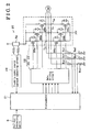
- Fig. 2 is a block view of the control substrate illustrated in Fig. 1;
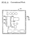
- Fig. 3 is a plan view illustrating a conventional internal structure of an ECU having a control substrate with a switching element fixed to a heat sink.
- a heat sink mounting a switching element thereon is equipped at a control substrate 20 of an ECU (electronic control unit) 10 controlling an electric power steering.
- the ECU 10 has the control substrate 20 and a housing case 30 housing the control substrate 20 therein.
- the control substrate 20 has a substrate 20a and various types of electrical components.
- the control substrate 20 includes a microcomputer 21 and a motor driving circuit 22. Signals detected by various types of detecting units are inputted into the microcomputer 21.
- the microcomputer 21 computes a control value based upon the detected signals. Further, the microcomputer 21 computes PWM (pulse width modulation) value for a motor M based upon the control value. Accordingly, the motor M can be driven in response to the PWM value transmitted from the microcomputer 21 through the motor driving circuit 22.
- the motor M is a three-phase synchronous type brushless motor having permanent magnets, as a non-limiting example.
- the motor driving circuit 22 includes a gate driving circuit 23 and an inverter circuit 24.
- the inverter circuit 24 is equipped with plural switching elements; three switching elements 25a, 25b, and 25c arranged at an upstream thereof, and the other three switching elements 26a, 26b, and 26c arranged at a downstream thereof.
- Each of the switching elements 25a, 25b, 25c, 26a, 26b, and 26c is a MOSFET (metal oxide semiconductor field-effect transistor), as a non-limiting example.
- a drain terminal of each switching element 25a, 25b, and 25c at the upper side is connected to a battery as a DC power source via a shunt resistance Rs, a gate terminal thereof is connected to the gate driving circuit 23, and a source terminal thereof is connected to a drain terminal of each switching element 26a, 26b, and 26c.
- a gate terminal of each switching element 26a, 26b, and 26c at the lower side is also connected to the gate driving circuit 23, and a source terminal thereof is grounded.
- the motor M is provided with three field wires; a U-phase wire, a V-phase wire, and a W-phase wire that are not shown.
- U-phase wire, V-phase wire, and W-phase wire are respectively connected to intermediate points Tu, Tv, and Tw between the switching elements 25a and 26a, the switching elements 25b and 26b, and the switching elements 25c and 26c.
- the intermediate points Tu, Tv, and Tw are grounded via first and second resistances Ru1 and Ru2, via first and second resistances Rv1 and via Rv2, and via first and second resistances Rw1 and Rw2, respectively.
- Each voltage between the first and second resistances Ru1 and Ru2, between the first and second resistances Rv1 and Rv2, and between the first and second resistances Rw1 and Rw2 corresponds to voltage generated by dividing motor terminal voltage of the U-phase, V-phase and W-phase.
- the voltage between each resistance can be inputted into the microcomputer 21.
- An electric power source current detecting circuit 28 connected to the shunt resistance Rs detects a value of voltage of the shunt resistance Rs, calculates a value of current applied to the motor M based upon the voltage value of the shunt resistance Rs. The current value can be inputted into the microcomputer 21.
- the microcomputer 21 switches on and off the switching elements 26a, 26b, and 26c (i.e., at least one first switching element) at a relatively high speed in accordance with duty control, and switches on and off the switching elements 25a, 25b, and 25c (i.e., at least one second switching elements) at a relatively low speed.
- Any of the switching elements heat up due to switching on and off.
- the switching elements 26a, 26b, and 26c heat up greatly among all the switching elements. Therefore, in order to radiate heat of the switching elements, the heat sink 27 is provided at the control substrate 20. More particularly, the switching elements 25a, 25b, 25c, 26a, 26b, and 26c are mounted at a substrate 20a of the control substrate 20. These switching elements are fixed to the heat sink at an upper surface of the substrate 20a.
- the high-speed switching element is switched on and off using PWM control with a predetermined duty ratio for a first predetermined period of time.
- the high-speed switching element is then switched off for a second predetermined period of time following the first period of time.
- the high-speed switching element is alternately shifted between the state being applied with the PWM control and the state not being applied with voltage.
- the low-speed switching element can be kept under an on condition for the first predetermined period of time while the high-speed switching element has been controlled by the PWM control. That is, the low-speed switching element can be switched on and off at fewer switching operations than the one of the high-speed switching element and at a longer cycle than the one of the high-speed switching element.
- the heat sink 27 has a substantially rectangular shape.
- the switching elements 25a, 25b, 25c, 26a, 26b, and 26c are fixed to the heat sink 27 without being one-sided. As illustrated in Fig. 1, the switching elements 26a, 26b, and 25c are fixed to one side surface 27a of the heat sink 27, which is located at an outside of the control substrate 20.
- the switching elements 26a, 25c, and 26b can be preferably arranged in this sequence at the side surface 27a.
- the switching elements 25a, 25b, and 26c are fixed to the other side surface 27b of the heat sink 27, which is located at an inside of the control substrate 20.
- the switching elements 25a, 26c, and 25b can be preferably arranged in this sequence at the side surface 27b.
- the high-speed switching element and the low-speed switching element can be arranged alternately.
- the high-speed switching elements do not have to be concentrated. Therefore, it can effectively prevent heat radiating performance of the heat sink 27 from being deteriorated and avoid influence to adjacent electrical components due to high temperature as much as possible.
- the heat sink 27 is arranged at an end portion of the substrate 20a rather than at a central portion thereof.
- the heat sink 27 has the substantially rectangular shape.
- the heat sink 27 can possess a cross section of a U-shaped structure or the like. Whichever shape the heat sink 27 has, it is preferable to provide a heat-radiating fin.
- the substrate 20a is provided not only with the above-described switching elements and the heat sink 27 but also with other electrical components such as the shunt resistance Rs, condensers C1 through C5, a coil CL1, and relays RL1 through RL4, as non-limiting examples.
- the high-speed switching elements 26a, 26b, and 26c are arranged at a distance from these electrical components. Therefore, it enables to more reliably prevent the adjacent electrical components from being influenced due to high temperature.
- the high-speed switching elements 26a and 26b can be arranged at the one side surface 27a of the heat sink 27. There are fewer electrical components mounted near the one side surface 27a of the heat sink 27 rather than near the other side surface 27b thereof. Therefore, it enables to more reliably prevent the adjacent electrical components from being influenced due to high temperature.
- the switching element is formed with the MOSFET.
- the switching element can be formed with a bipolar type transistor or IGBT (insulated gate bipolar transistor), as non-limiting examples.
- the motor M is formed with a three-phase synchronous type brushless motor having permanent magnets.
- the motor M can be formed with a synchronous permanent magnet motor as a non-limiting example.
- the motor M does not have to be limited to the brushless motor and can be a DC motor as a non-limiting example.
- control substrate 20 equipped with the heat sink and the switching elements is applied to the ECU 10 for controlling the electric power steering.
- the control substrate 20 equipped with the heat sink and the switching elements can be applied to other types of control unit for controlling a motor.
- the switching elements 25a, 25b, and 25c at the upper side are the low-speed switching elements
- the switching elements 26a, 26b, and 26c at the lower side are the high-speed switching elements
- the switching elements 25a, 25b, and 25c at the upper side can be the high-speed switching elements
- the switching elements 26a, 26b, and 26c at the lower side can be the low-speed switching elements.
- An electronic control unit has a driving circuit for driving a motor by a PWM control, a heat sink provided at a substrate of the electronic control unit, at least one first switching element equipped to the driving circuit and switched on and off at a relatively high speed by the driving circuit, and at least one second switching element equipped to the driving circuit and switched on and off at a relatively low speed by the driving circuit.
- the at least one first switching element and the at least one second switching element are alternately arranged and fixed to the heat sink.
Landscapes
- Engineering & Computer Science (AREA)
- Power Engineering (AREA)
- Inverter Devices (AREA)
- Power Steering Mechanism (AREA)
- Cooling Or The Like Of Electrical Apparatus (AREA)
- Cooling Or The Like Of Semiconductors Or Solid State Devices (AREA)
- Control Of Motors That Do Not Use Commutators (AREA)
Abstract
Description
- This invention generally relates to a mounting structure of a switching element at a heat sink.
- A motor driving circuit, which is configured with plural switching elements and controls a motor by a PWM (pulse width modulation) control, has been conventionally known. In the motor driving circuit, the plural switching elements are mounted at a heat sink. With reference to Figs. 2 and 3, the mounting structure of the plural switching elements at the heat sink is described below. The heat sink is equipped at a
control substrate 20 of an ECU (electronic control unit) 10, - As illustrated in FIG. 3, the ECU 10 includes the
control substrate 20 and ahousing case 30 housing thecontrol substrate 20 therein. As illustrated in FIG. 2, thecontrol substrate 20 includes amicrocomputer 21 and amotor driving circuit 22. Signals detected by various types of detecting units are inputted into themicrocomputer 21. Themicrocomputer 21 computes a control value based upon the detected signals. Further, themicrocomputer 21 computes the PWM value for a motor M based upon the control value. Accordingly, the motor M can be driven in response to the PWM value transmitted from themicrocomputer 21 through themotor driving circuit 22. - The
motor driving circuit 22 includes agate driving circuit 23 and aninverter circuit 24. According to an embodiment of the present invention, theinverter circuit 24 includes plural switching elements; threeswitching elements switching elements switching elements switching element gate driving circuit 23, and a source terminal thereof is connected to a drain terminal of eachswitching element switching element gate driving circuit 23, and a source terminal thereof is grounded. The motor M includes three field wires; a U-phase wire, a V-phase wire, and a W-phase wire that are not shown. These U-phase wire, V-phase wire, and W-phase wire are connected to intermediate points Tu, Tv, and Tw between theswitching elements switching elements switching elements microcomputer 21. - In order to drive the motor M by the
ECU 10 with the above described structure, themicrocomputer 21 switches on and off theswitching elements switching elements switching elements heat sink 27 is provided at thecontrol substrate 20. More particularly, theswitching elements substrate 20a of thecontrol substrate 20. These switching elements are fixed to the heat sink at an upper surface of thesubstrate 20a. - However, as illustrated in FIG. 3, the high-
speed switching elements heat sink 27, and the low-speed switching elements speed switching elements heat sink 27. In this case, heat radiating performance of theheat sink 27 may become deteriorated. Further, it may become inevitable that electrical components around theheat sink 27 may be influenced due to high temperature. - The present invention exists for providing an improved unit having a heat sink and high-speed switching elements arranged without being concentrated, thereby effectively reducing deterioration of heart radiating performance of the heat sink and avoiding temperature influence to adjacent electrical components as much as possible.
- According to an aspect of the present invention, an electronic control unit has a driving circuit for driving a motor by a PWM control, a heat sink provided at a substrate of the electronic control unit, at least one first switching element equipped to the driving circuit and switched on and off at a relatively high speed by the driving circuit, and at least one second switching element equipped to the driving circuit and switched on and off at a relatively low speed by the driving circuit. The at least one first switching element and the at least one second switching element are alternately arranged and fixed to the heat sink.
- It is preferable that the at least one first switching element is fixed to the heat sink at a distant from other electrical components at the substrate of the electronic control unit.
- The foregoing and additional features and characteristics of the present invention will become more apparent from the following detailed description considered with reference to the accompanying drawings, wherein:
- Fig. 1 is a plan view illustrating an internal structure of an ECU having a control substrate with switching elements fixed to a heat sink according to an embodiment of the present invention;
- Fig. 2 is a block view of the control substrate illustrated in Fig. 1; and
- Fig. 3 is a plan view illustrating a conventional internal structure of an ECU having a control substrate with a switching element fixed to a heat sink.
- As illustrated in Figs. 1 and 2, according to an embodiment of the present invention, a heat sink mounting a switching element thereon is equipped at a
control substrate 20 of an ECU (electronic control unit) 10 controlling an electric power steering. The ECU 10 has thecontrol substrate 20 and ahousing case 30 housing thecontrol substrate 20 therein. Thecontrol substrate 20 has asubstrate 20a and various types of electrical components. As illustrated in FIG. 2, thecontrol substrate 20 includes amicrocomputer 21 and amotor driving circuit 22. Signals detected by various types of detecting units are inputted into themicrocomputer 21. Themicrocomputer 21 computes a control value based upon the detected signals. Further, themicrocomputer 21 computes PWM (pulse width modulation) value for a motor M based upon the control value. Accordingly, the motor M can be driven in response to the PWM value transmitted from themicrocomputer 21 through themotor driving circuit 22. The motor M is a three-phase synchronous type brushless motor having permanent magnets, as a non-limiting example. - The
motor driving circuit 22 includes agate driving circuit 23 and aninverter circuit 24. According to the embodiment of the present invention, theinverter circuit 24 is equipped with plural switching elements; threeswitching elements switching elements switching elements switching element gate driving circuit 23, and a source terminal thereof is connected to a drain terminal of eachswitching element switching element gate driving circuit 23, and a source terminal thereof is grounded. The motor M is provided with three field wires; a U-phase wire, a V-phase wire, and a W-phase wire that are not shown. These U-phase wire, V-phase wire, and W-phase wire are respectively connected to intermediate points Tu, Tv, and Tw between theswitching elements switching elements switching elements microcomputer 21. An electric power sourcecurrent detecting circuit 28 connected to the shunt resistance Rs detects a value of voltage of the shunt resistance Rs, calculates a value of current applied to the motor M based upon the voltage value of the shunt resistance Rs. The current value can be inputted into themicrocomputer 21. - In order to drive the motor M by the
ECU 10 with the above described structure, themicrocomputer 21 switches on and off theswitching elements switching elements switching elements heat sink 27 is provided at thecontrol substrate 20. More particularly, theswitching elements substrate 20a of thecontrol substrate 20. These switching elements are fixed to the heat sink at an upper surface of thesubstrate 20a. - The high-speed switching element is switched on and off using PWM control with a predetermined duty ratio for a first predetermined period of time. The high-speed switching element is then switched off for a second predetermined period of time following the first period of time. As aforementioned, the high-speed switching element is alternately shifted between the state being applied with the PWM control and the state not being applied with voltage. In the meantime, the low-speed switching element can be kept under an on condition for the first predetermined period of time while the high-speed switching element has been controlled by the PWM control. That is, the low-speed switching element can be switched on and off at fewer switching operations than the one of the high-speed switching element and at a longer cycle than the one of the high-speed switching element.
- According to the embodiment of the present invention, the
heat sink 27 has a substantially rectangular shape. Theswitching elements heat sink 27 without being one-sided. As illustrated in Fig. 1, theswitching elements side surface 27a of theheat sink 27, which is located at an outside of thecontrol substrate 20. Theswitching elements side surface 27a. Theswitching elements other side surface 27b of theheat sink 27, which is located at an inside of thecontrol substrate 20. Theswitching elements side surface 27b. That is, the high-speed switching element and the low-speed switching element can be arranged alternately. In other words, the high-speed switching elements do not have to be concentrated. Therefore, it can effectively prevent heat radiating performance of theheat sink 27 from being deteriorated and avoid influence to adjacent electrical components due to high temperature as much as possible. - Further, it is preferable that the
heat sink 27 is arranged at an end portion of thesubstrate 20a rather than at a central portion thereof. According to the embodiment of the present invention, theheat sink 27 has the substantially rectangular shape. Alternatively, theheat sink 27 can possess a cross section of a U-shaped structure or the like. Whichever shape theheat sink 27 has, it is preferable to provide a heat-radiating fin. - The
substrate 20a is provided not only with the above-described switching elements and theheat sink 27 but also with other electrical components such as the shunt resistance Rs, condensers C1 through C5, a coil CL1, and relays RL1 through RL4, as non-limiting examples. The high-speed switching elements - As described above, according to the embodiment of the present invention, the high-
speed switching elements side surface 27a of theheat sink 27. There are fewer electrical components mounted near the oneside surface 27a of theheat sink 27 rather than near theother side surface 27b thereof. Therefore, it enables to more reliably prevent the adjacent electrical components from being influenced due to high temperature. - According to the embodiment of the present invention, the switching element is formed with the MOSFET. Alternatively, the switching element can be formed with a bipolar type transistor or IGBT (insulated gate bipolar transistor), as non-limiting examples.
- Further, according to the embodiment of the present invention, the motor M is formed with a three-phase synchronous type brushless motor having permanent magnets. Alternatively, the motor M can be formed with a synchronous permanent magnet motor as a non-limiting example. Further, the motor M does not have to be limited to the brushless motor and can be a DC motor as a non-limiting example.
- Still further, according to the embodiment of the present invention, the
control substrate 20 equipped with the heat sink and the switching elements is applied to theECU 10 for controlling the electric power steering. Alternatively, thecontrol substrate 20 equipped with the heat sink and the switching elements can be applied to other types of control unit for controlling a motor. - Still further, according to the embodiment of the present invention, the
switching elements switching elements switching elements switching elements
An electronic control unit has a driving circuit for driving a motor by a PWM control, a heat sink provided at a substrate of the electronic control unit, at least one first switching element equipped to the driving circuit and switched on and off at a relatively high speed by the driving circuit, and at least one second switching element equipped to the driving circuit and switched on and off at a relatively low speed by the driving circuit. The at least one first switching element and the at least one second switching element are alternately arranged and fixed to the heat sink.
Claims (5)
- An electronic control unit comprising:wherein the at least one first switching element and the at least one second switching element are alternately arranged and fixed to the heat sink.a driving circuit for driving a motor;a heat sink provided at a substrate of the electronic control unit;at least one first switching element equipped to the driving circuit and switched on and off at a relatively high speed by the driving circuit; andat least one second switching element equipped to the driving circuit and switched on and off at a relatively low speed by the driving circuit,
- An electronic control unit according to claim 1, wherein the heat sink has one surface near outside of the substrate and an other surface near a central portion of the substrate, the at least one first switching element is fixed to the one surface, and the at least one second switching element is fixed to the other surface.
- An electronic control unit according to claim 1, wherein the heat sink has one surface near outside of the substrate and an other surface near a central portion of the substrate; the at least one first switching elements and the at least one second switching elements are alternately arranged at the one surface and the other surface of the heat sink.
- An electronic control unit according to claim 1, wherein the at least one first switching element is fixed to the heat sink at a distant from other electrical components at the substrate of the electronic control unit.
- An electronic control unit according to claim 1, wherein the driving circuit drives the motor by a PWM control.
Applications Claiming Priority (2)
| Application Number | Priority Date | Filing Date | Title |
|---|---|---|---|
| JP2003150878A JP2004357384A (en) | 2003-05-28 | 2003-05-28 | Switching element mounting structure to heat sink |
| JP2003150878 | 2003-05-28 |
Publications (1)
| Publication Number | Publication Date |
|---|---|
| EP1482631A2 true EP1482631A2 (en) | 2004-12-01 |
Family
ID=33128249
Family Applications (1)
| Application Number | Title | Priority Date | Filing Date |
|---|---|---|---|
| EP20040012644 Withdrawn EP1482631A2 (en) | 2003-05-28 | 2004-05-27 | Mounting structure of a switching element at a heat sink |
Country Status (3)
| Country | Link |
|---|---|
| US (1) | US20040239278A1 (en) |
| EP (1) | EP1482631A2 (en) |
| JP (1) | JP2004357384A (en) |
Cited By (1)
| Publication number | Priority date | Publication date | Assignee | Title |
|---|---|---|---|---|
| US20140312721A1 (en) * | 2008-09-26 | 2014-10-23 | Makita Corporation | Electric power tool including a plurality of circuit boards |
Families Citing this family (6)
| Publication number | Priority date | Publication date | Assignee | Title |
|---|---|---|---|---|
| JP4553032B2 (en) * | 2008-05-12 | 2010-09-29 | 株式会社デンソー | Load drive device |
| JP5593074B2 (en) * | 2010-01-06 | 2014-09-17 | 矢崎総業株式会社 | Heat sink mounting structure |
| JP2015084622A (en) | 2013-10-25 | 2015-04-30 | 三菱重工オートモーティブサーマルシステムズ株式会社 | Driving device and driving method for switching element; and vehicular air conditioner |
| KR102599388B1 (en) * | 2017-09-01 | 2023-11-09 | 현대자동차주식회사 | Feedback control method and system |
| JP2018019419A (en) * | 2017-09-29 | 2018-02-01 | 日本電波工業株式会社 | Piezoelectric oscillator |
| WO2021039753A1 (en) * | 2019-08-28 | 2021-03-04 | パナソニックIpマネジメント株式会社 | Ventilation device |
Family Cites Families (24)
| Publication number | Priority date | Publication date | Assignee | Title |
|---|---|---|---|---|
| US4646203A (en) * | 1985-02-06 | 1987-02-24 | Lutron Electronics Co., Inc. | Mounting structure for semiconductor devices |
| JP2626326B2 (en) * | 1991-07-31 | 1997-07-02 | 三菱電機株式会社 | Motor control unit |
| US5579217A (en) * | 1991-07-10 | 1996-11-26 | Kenetech Windpower, Inc. | Laminated bus assembly and coupling apparatus for a high power electrical switching converter |
| US5504378A (en) * | 1994-06-10 | 1996-04-02 | Westinghouse Electric Corp. | Direct cooled switching module for electric vehicle propulsion system |
| JPH09148523A (en) * | 1995-11-21 | 1997-06-06 | Toshiba Corp | Semiconductor device |
| JP3406753B2 (en) * | 1995-11-30 | 2003-05-12 | 三菱電機株式会社 | Semiconductor device and semiconductor module |
| JP3345241B2 (en) * | 1995-11-30 | 2002-11-18 | 三菱電機株式会社 | Semiconductor device |
| US5801937A (en) * | 1996-10-16 | 1998-09-01 | American Superconductor Corporation | Uninterruptible power supplies having cooled components |
| US6462976B1 (en) * | 1997-02-21 | 2002-10-08 | University Of Arkansas | Conversion of electrical energy from one form to another, and its management through multichip module structures |
| GB2330254B (en) * | 1997-10-09 | 2000-10-18 | Toshiba Kk | Multiple inverter system |
| US5872711A (en) * | 1998-01-20 | 1999-02-16 | Reliance Electric Industrial Company | Low impedance contoured laminated bus assembly and method for making same |
| AU2765599A (en) * | 1998-02-13 | 1999-08-30 | Wisconsin Alumni Research Foundation | Hybrid topology for multilevel power conversion |
| US5933339A (en) * | 1998-03-23 | 1999-08-03 | Electric Boat Corporation | Modular static power converter connected in a multi-level, multi-phase, multi-circuit configuration |
| US6072707A (en) * | 1998-10-23 | 2000-06-06 | Siemens Power Transmission & Distribution, Inc. | High voltage modular inverter |
| US6060788A (en) * | 1998-11-12 | 2000-05-09 | Eaton Corporation | Vehicle driver module |
| US6236580B1 (en) * | 1999-04-09 | 2001-05-22 | Robicon Corporation | Modular multi-level adjustable supply with series connected active inputs |
| JP4054137B2 (en) * | 1999-06-03 | 2008-02-27 | 株式会社東京アールアンドデー | Power semiconductor element power supply and heat dissipation device |
| US6396137B1 (en) * | 2000-03-15 | 2002-05-28 | Kevin Mark Klughart | Integrated voltage/current/power regulator/switch system and method |
| US6697271B2 (en) * | 2000-08-16 | 2004-02-24 | Northrop Grumman Corporation | Cascaded multi-level H-bridge drive |
| US6847531B2 (en) * | 2001-01-02 | 2005-01-25 | General Electric Company | System and method for regenerative PWM AC power conversion |
| JP2002359329A (en) * | 2001-05-30 | 2002-12-13 | Hitachi Ltd | Semiconductor device |
| EP1263046A1 (en) * | 2001-06-01 | 2002-12-04 | ABB Schweiz AG | Contact Arrangement |
| US6833617B2 (en) * | 2001-12-18 | 2004-12-21 | Hitachi, Ltd. | Composite material including copper and cuprous oxide and application thereof |
| US6788033B2 (en) * | 2002-08-08 | 2004-09-07 | Vlt, Inc. | Buck-boost DC-DC switching power conversion |
-
2003
- 2003-05-28 JP JP2003150878A patent/JP2004357384A/en active Pending
-
2004
- 2004-05-27 EP EP20040012644 patent/EP1482631A2/en not_active Withdrawn
- 2004-05-28 US US10/855,638 patent/US20040239278A1/en not_active Abandoned
Cited By (3)
| Publication number | Priority date | Publication date | Assignee | Title |
|---|---|---|---|---|
| US20140312721A1 (en) * | 2008-09-26 | 2014-10-23 | Makita Corporation | Electric power tool including a plurality of circuit boards |
| EP2845690A3 (en) * | 2008-09-26 | 2015-05-20 | Makita Corporation | Electric power tool |
| US9621009B2 (en) | 2008-09-26 | 2017-04-11 | Makita Corporation | Electric power tool including a plurality of circuit boards |
Also Published As
| Publication number | Publication date |
|---|---|
| JP2004357384A (en) | 2004-12-16 |
| US20040239278A1 (en) | 2004-12-02 |
Similar Documents
| Publication | Publication Date | Title |
|---|---|---|
| US7961472B2 (en) | Electric circuit device, electric circuit module, and power converter | |
| US10106189B2 (en) | Motor drive control device for electric power steering | |
| US8564996B2 (en) | Semiconductor module and driving apparatus including semiconductor module | |
| US6166464A (en) | Power module | |
| US8045335B2 (en) | Semiconductor device | |
| US8796971B2 (en) | Motor drive apparatus | |
| US20030107120A1 (en) | Intelligent motor drive module with injection molded package | |
| US9123711B2 (en) | Wiring member and semiconductor module having the same | |
| US7864533B2 (en) | Semiconductor device | |
| US9231466B2 (en) | Electronic circuit | |
| EP3240185B1 (en) | Motor driving control apparatus with winding changeover switch of motor, motor, compressor, and method of controlling winding changeover of motor | |
| JP6627637B2 (en) | Electronic circuit | |
| KR20160021825A (en) | Inverter for an electric motor or generator | |
| US8896171B2 (en) | Motor drive apparatus having a simplified assembling structure | |
| US12494416B2 (en) | Semiconductor module with non-common wiring electrode and common wiring region | |
| US20040239278A1 (en) | Mounting structure of a switching element at a heat sink | |
| JP2021090328A (en) | Inverter controller | |
| JP4064741B2 (en) | Semiconductor device | |
| EP2779811A1 (en) | Drive circuit device | |
| JP3922698B2 (en) | Semiconductor device | |
| JP2008048503A (en) | Inverter module | |
| JPH10229681A (en) | Switching device for electric vehicles | |
| KR20100106814A (en) | Driver device | |
| US20120286594A1 (en) | Motor drive apparatus | |
| KR20220087955A (en) | Motor control circuit |
Legal Events
| Date | Code | Title | Description |
|---|---|---|---|
| PUAI | Public reference made under article 153(3) epc to a published international application that has entered the european phase |
Free format text: ORIGINAL CODE: 0009012 |
|
| AK | Designated contracting states |
Kind code of ref document: A2 Designated state(s): AT BE BG CH CY CZ DE DK EE ES FI FR GB GR HU IE IT LI LU MC NL PL PT RO SE SI SK TR |
|
| AX | Request for extension of the european patent |
Extension state: AL HR LT LV MK |
|
| RAP1 | Party data changed (applicant data changed or rights of an application transferred) |
Owner name: JTEKT CORPORATION |
|
| RIN1 | Information on inventor provided before grant (corrected) |
Inventor name: USHIROYAMA, MITSUYA Inventor name: WATANABE, YUKIHIRO Inventor name: KOBAYASHI, YUKIHIRO |
|
| STAA | Information on the status of an ep patent application or granted ep patent |
Free format text: STATUS: THE APPLICATION HAS BEEN WITHDRAWN |
|
| 18W | Application withdrawn |
Effective date: 20090916 |