EP1482573A2 - Organic electroluminescence device - Google Patents
Organic electroluminescence device Download PDFInfo
- Publication number
- EP1482573A2 EP1482573A2 EP04012472A EP04012472A EP1482573A2 EP 1482573 A2 EP1482573 A2 EP 1482573A2 EP 04012472 A EP04012472 A EP 04012472A EP 04012472 A EP04012472 A EP 04012472A EP 1482573 A2 EP1482573 A2 EP 1482573A2
- Authority
- EP
- European Patent Office
- Prior art keywords
- group
- organic electroluminescence
- electroluminescence device
- light
- organic
- Prior art date
- Legal status (The legal status is an assumption and is not a legal conclusion. Google has not performed a legal analysis and makes no representation as to the accuracy of the status listed.)
- Withdrawn
Links
- 0 C*1COCC1 Chemical compound C*1COCC1 0.000 description 4
Images

Classifications
-
- H—ELECTRICITY
- H10—SEMICONDUCTOR DEVICES; ELECTRIC SOLID-STATE DEVICES NOT OTHERWISE PROVIDED FOR
- H10K—ORGANIC ELECTRIC SOLID-STATE DEVICES
- H10K85/00—Organic materials used in the body or electrodes of devices covered by this subclass
- H10K85/60—Organic compounds having low molecular weight
- H10K85/615—Polycyclic condensed aromatic hydrocarbons, e.g. anthracene
- H10K85/626—Polycyclic condensed aromatic hydrocarbons, e.g. anthracene containing more than one polycyclic condensed aromatic rings, e.g. bis-anthracene
-
- C—CHEMISTRY; METALLURGY
- C09—DYES; PAINTS; POLISHES; NATURAL RESINS; ADHESIVES; COMPOSITIONS NOT OTHERWISE PROVIDED FOR; APPLICATIONS OF MATERIALS NOT OTHERWISE PROVIDED FOR
- C09K—MATERIALS FOR MISCELLANEOUS APPLICATIONS, NOT PROVIDED FOR ELSEWHERE
- C09K11/00—Luminescent, e.g. electroluminescent, chemiluminescent materials
- C09K11/06—Luminescent, e.g. electroluminescent, chemiluminescent materials containing organic luminescent materials
-
- H—ELECTRICITY
- H05—ELECTRIC TECHNIQUES NOT OTHERWISE PROVIDED FOR
- H05B—ELECTRIC HEATING; ELECTRIC LIGHT SOURCES NOT OTHERWISE PROVIDED FOR; CIRCUIT ARRANGEMENTS FOR ELECTRIC LIGHT SOURCES, IN GENERAL
- H05B33/00—Electroluminescent light sources
- H05B33/12—Light sources with substantially two-dimensional radiating surfaces
- H05B33/14—Light sources with substantially two-dimensional radiating surfaces characterised by the chemical or physical composition or the arrangement of the electroluminescent material, or by the simultaneous addition of the electroluminescent material in or onto the light source
-
- H—ELECTRICITY
- H10—SEMICONDUCTOR DEVICES; ELECTRIC SOLID-STATE DEVICES NOT OTHERWISE PROVIDED FOR
- H10K—ORGANIC ELECTRIC SOLID-STATE DEVICES
- H10K50/00—Organic light-emitting devices
- H10K50/10—OLEDs or polymer light-emitting diodes [PLED]
- H10K50/11—OLEDs or polymer light-emitting diodes [PLED] characterised by the electroluminescent [EL] layers
- H10K50/125—OLEDs or polymer light-emitting diodes [PLED] characterised by the electroluminescent [EL] layers specially adapted for multicolour light emission, e.g. for emitting white light
-
- H—ELECTRICITY
- H10—SEMICONDUCTOR DEVICES; ELECTRIC SOLID-STATE DEVICES NOT OTHERWISE PROVIDED FOR
- H10K—ORGANIC ELECTRIC SOLID-STATE DEVICES
- H10K85/00—Organic materials used in the body or electrodes of devices covered by this subclass
- H10K85/30—Coordination compounds
- H10K85/321—Metal complexes comprising a group IIIA element, e.g. Tris (8-hydroxyquinoline) gallium [Gaq3]
- H10K85/324—Metal complexes comprising a group IIIA element, e.g. Tris (8-hydroxyquinoline) gallium [Gaq3] comprising aluminium, e.g. Alq3
-
- H—ELECTRICITY
- H10—SEMICONDUCTOR DEVICES; ELECTRIC SOLID-STATE DEVICES NOT OTHERWISE PROVIDED FOR
- H10K—ORGANIC ELECTRIC SOLID-STATE DEVICES
- H10K85/00—Organic materials used in the body or electrodes of devices covered by this subclass
- H10K85/60—Organic compounds having low molecular weight
- H10K85/615—Polycyclic condensed aromatic hydrocarbons, e.g. anthracene
- H10K85/622—Polycyclic condensed aromatic hydrocarbons, e.g. anthracene containing four rings, e.g. pyrene
-
- H—ELECTRICITY
- H10—SEMICONDUCTOR DEVICES; ELECTRIC SOLID-STATE DEVICES NOT OTHERWISE PROVIDED FOR
- H10K—ORGANIC ELECTRIC SOLID-STATE DEVICES
- H10K85/00—Organic materials used in the body or electrodes of devices covered by this subclass
- H10K85/60—Organic compounds having low molecular weight
- H10K85/631—Amine compounds having at least two aryl rest on at least one amine-nitrogen atom, e.g. triphenylamine
- H10K85/633—Amine compounds having at least two aryl rest on at least one amine-nitrogen atom, e.g. triphenylamine comprising polycyclic condensed aromatic hydrocarbons as substituents on the nitrogen atom
-
- Y—GENERAL TAGGING OF NEW TECHNOLOGICAL DEVELOPMENTS; GENERAL TAGGING OF CROSS-SECTIONAL TECHNOLOGIES SPANNING OVER SEVERAL SECTIONS OF THE IPC; TECHNICAL SUBJECTS COVERED BY FORMER USPC CROSS-REFERENCE ART COLLECTIONS [XRACs] AND DIGESTS
- Y10—TECHNICAL SUBJECTS COVERED BY FORMER USPC
- Y10S—TECHNICAL SUBJECTS COVERED BY FORMER USPC CROSS-REFERENCE ART COLLECTIONS [XRACs] AND DIGESTS
- Y10S428/00—Stock material or miscellaneous articles
- Y10S428/917—Electroluminescent
Definitions
- the present invention relates to an organic electroluminescence device having a simple layered structure and emitting white or substantially white light.
- An organic electroluminescence device is a device which itself emits light, and has features such that it can emit light with wide viewing angle and high luminance and can be reduced in thickness, and therefore, application of the device to next-generation flat display or its flat light source has attracted attention.
- the method for achieving full-color display using the organic electroluminescence device may be roughly classified into the following three methods.
- the first one is a method in which light emitting portions respectively for red (R) , green (G) , and blue (B) are formed on a flat surface, for example, by a resistance heating deposition method using a metal mask.
- RGB i.e., three types of elements (subpixels) are individually formed on the same substrate and combined to form one pixel. Therefore, there is a need to prepare a deposition mask having a fine pattern for pixels and align it on the substrate with high accuracy, causing a problem in that the productivity is low and the cost is high in the manufacturing process.
- the second one is a method in which full-color display is made using an organic light-emitting layer which emits monochromatic light, for example, blue light, and a color changing layer, provided on the forward side as viewed in the light emitting direction, for changing the blue light to red or green light.
- an organic light-emitting layer which emits monochromatic light, for example, blue light
- a color changing layer provided on the forward side as viewed in the light emitting direction, for changing the blue light to red or green light.
- the third one is a method in which light emitted from an organic electroluminescence device emitting white light is divided into RGB using a color filter.
- the method of obtaining arbitrary light by using the white-light emitting layer and the color filter in combination there is no need to align a deposition mask to produce individual colors of light, and therefore the number of manufacturing steps may be reduced, making it possible to improve the productivity in the manufacturing process and suppress the cost.
- Examples of methods for obtaining white light emission include: (1) a method using RGB light emitting layers in combination; (2) a method for allowing a single or a plurality of light emitting layers to emit light having two wavelengths which have the relationship of complementary colors, i.e., bluish green and red light, or blue and yellow to orange light; and (3) a method utilizing exciplex emission.
- a method using RGB light emitting layers in combination a method for allowing a single or a plurality of light emitting layers to emit light having two wavelengths which have the relationship of complementary colors, i.e., bluish green and red light, or blue and yellow to orange light
- a method utilizing exciplex emission As the method (1) above, a method in which blue-, green-, and red-light emitting layers are stacked on one another to obtain white light has been proposed (e.g., Japanese Patent Application Publication No. 07-142169).
- the method (2) above includes a method in which two light-emitting layers for individual colors are stacked (e
- an organic electroluminescence device which includes an organic layer having a light emission region and being disposed between an anode and a cathode.
- the organic layer contains, as an organic light-emitting material, a compound represented by the following formula (1): where each of R 1 to R 26 independently represents a substituent arbitrarily selected from a hydrogen atom, a halogen atom, a hydroxyl group, a mercapto group, a nitro group, an amino group, a cyano group, an alkyl group, an alkenyl group, a cycloalkyl group, an alkoxy group, an alkylthio group, a silyl group, an alkylsilyl group, a siloxanyl group, an aralkyl group, an aromatic hydrocarbon group, an aromatic heterocyclic group, an ester group, an aryloxy group, a formyl group, an alkoxycarbonyl group, and a carboxyl
- each of R 1 to R 26 independently represents a substituent arbitrarily selected from a hydrogen atom, an alkyl group, an alkoxy group, an aromatic hydrocarbon group, and an aromatic heterocyclic group.
- an organic electroluminescence device which emits white light.
- an organic electroluminescence device which includes an organic layer having a light emission region and being disposed between an anode and a cathode.
- the organic layer contains, as an organic light-emitting material, a compound represented by the following formula (2): where each of R 1 to R 26 independently represents a substituent arbitrarily selected from a hydrogen atom, a halogen atom, a hydroxyl group, a mercapto group, a nitro group, an amino group, a cyano group, an alkyl group, an alkenyl group, a cycloalkyl group, an alkoxy group, an alkylthio group, a silyl group, an alkylsilyl group, a siloxanyl group, an aralkyl group, an aromatic hydrocarbon group, an aromatic heterocyclic group, an ester group, an aryloxy group, a formyl group, an alkoxycarbonyl group, and a carboxyl
- each of R 1 to R 26 independently represents a substituent arbitrarily selected from a hydrogen atom, an alkyl group, an alkoxy group, an aromatic hydrocarbon group, and an aromatic heterocyclic group.
- an organic electroluminescence device according to the fifth aspect, which emits white light.
- an organic electroluminescence device according to the fourth aspect, wherein, as the compound represented by the formula (2) above, a compound represented by the following structural formula (3) is used:
- an organic electroluminescence device according to the fourth aspect, wherein, as the compound represented by the formula (2) above, a compound represented by the following structural formula (4) is used:
- an organic electroluminescence device according to the fourth aspect, wherein, as the compound represented by the formula (2) above, a compound represented by the following structural formula (5) is used:
- the compound represented by the formula (1) above in the above-described aspect of the present invention is a compound which itself emits white or substantially white light, namely, a single compound having respective peak tops in the RGB regions. Therefore, by passing light emitted from a light emitting .material containing this compound through a color filter, the light may be divided into RGB individual pixels. Thus, an organic electroluminescence device having a simple layered structure can be prepared.
- an organic electroluminescence device whose productivity is higher and which has a simpler layered structure that can emits white or substantially white light.
- examples of an "organic layer having a light emission region” may include the following:
- the organic layer contains, as an organic light-emitting material, a compound
- the compound of the formula (1) is contained in at least one layer of the above-mentioned layers and contributes to the light emission.
- the compound of the formula (1) may be solely used, or the compound of the formula (1) as a dopant and a host material may used in combination.
- each of R 1 to R 26 independently represents a substituent arbitrarily selected from a hydrogen atom, a halogen atom, a hydroxyl group, a mercapto group, a nitro group, an amino group, a cyano group, an alkyl group, an alkenyl group, a cycloalkyl group, an alkoxy group, an alkylthio group, a silyl group, an alkylsilyl group, a siloxanyl group, an aralkyl group, an aromatic hydrocarbon group, an aromatic heterocyclic group, an ester group, an aryloxy group, a formyl group, an alkoxycarbonyl group, and a carboxyl group, and n 1 is a numeric value from 1 to 3, and it is preferred that each of R 1 to R 26 independently represents a substituent arbitrarily selected from a hydrogen atom, an alky
- n 1 is 1 ⁇ corresponding to the formula (2) above ⁇ , and, in this case, in the formula, each of R 1 to R 26 independently represents a substituent arbitrarily selected from a hydrogen atom, a halogen atom, a hydroxyl group, a mercapto group, a nitro group, an amino group, a cyano group, an alkyl group, an alkenyl group, a cycloalkyl group, an alkoxy group, an alkylthio group, a silyl group, an alkylsilyl group, a siloxanyl group, an aralkyl group, an aromatic hydrocarbon group, an aromatic heterocyclic group, an ester group, an aryloxy group, a formyl group, an alkoxycarbonyl group, and a carboxyl group. It is preferred that each of R 1 to R 26 independently represents a substituent arbitrarily selected from a hydrogen atom, an alkyl group, an al
- the number of carbon atoms contained in each of the alkyl group and the alkoxy group may be 20 or less.
- the number of carbon atoms contained in each of the aromatic hydrocarbon group and the aromatic heterocyclic group may be 30 or less.
- the following compound represented by structural formulae (1-1) to (1-4) may be used for the alkoxy group
- structural formulae (1-5) to (1-6) may be used for the aromatic hydrocarbon group (aryl group)
- structural formulae (1-7) to (1-8) for the aromatic heterocyclic group.
- the compound represented by the formula (1) or (2), especially the group of compounds represented by the structural formulae (3) to (30) has characteristic fluorescence wavelengths having respective peak tops in the RGB regions.
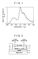
- a fluorescence spectrum of the compound of the structural formula (3) as a representative compound is shown in FIG. 1. As can be seen in FIG. 1, the compound has respective peak tops near the RGB regions, although the intensity in the B region is slightly low.
- the light By passing light emitted from the organic light-emitting material through a color filter, the light may be divided into RGB.
- a color filter on the organic electroluminescence device which includes the organic layer having a light emission region and being disposed between an anode and a cathode, wherein the light emitting layer contains, as the organic light-emitting material, at least one compound selected from the compounds represented by the formulae (1) and (2) , especially the compounds represented by the structural formulae (3) and (6) to (16), the light emitted from the device may be divided into RGB individual pixels.
- the organic electroluminescence device which includes the organic layer having a light emission region and being disposed between an anode and a cathode, wherein the light emitting layer contains, as the organic light-emitting material, at least one compound selected from the compounds represented by the formulae (1) and (2), especiallythe compounds represented by the structural formulae (3) and (6) to (16), the intensities of RGB can be made at the same level in order to obtain white light.
- the organic light-emitting material may be either solely used in the light emitting layer or used in combination with a blue-light emitting layer made of a blue-light material, which appropriately corrects the spectrum in the B (blue) region, to form a layered structure.
- the organic light-emitting material may be the combination of a host material and a dopant.
- a light emitting material emitting blue light as a host and at least one light emitting material represented by the formula (1) as a dopant are used in combination in the light emitting layer to obtain white light.
- the light emitting layer may be of either a single layer or a layered structure.
- the compound in an embodiment of the present invention is generally contained in the light emitting layer as mentioned above, but it may be contained in another layer in the organic layer having a light emission region.
- RGB light emission can be obtained from a single chemical species. Therefore, there is provided a light emitting device which stably emits light without causing color drift, resulting in remarkable advantages from the viewpoint of the technique and cost in the manufacturing process. Further, white light can be obtained from the device having a considerably simple layered structure.
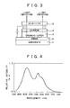
- FIG. 2 is a diagrammatic cross-sectional view of one example of an organic electroluminescence device according to the present embodiment.
- the organic electroluminescence device includes an anode 2, an organic layer 3 having a light emission region, and a cathode 4, which are formed on a substrate 1 in this order from bottom.
- This organic electroluminescence device is a top emission type organic electroluminescence device which emits light from the side of the cathode.
- the substrate 1 glass, a plastic, or another material may be used if it is applicable.
- the organic electroluminescence device and another display device are used in combination, the substrate 1 may be shared by them.
- the anode 2 one having a layered structure including an indium tin oxide (ITO) layer may be used.
- the organic layer 3 contains an organic light-emitting material represented by the formula (1) above.
- an organic light-emitting material represented by the formula (1) above As respect to the organic layer 3, as the construction of layers for obtaining organic electroluminescence, various types of constructions conventionally known may be employed. For example, if the material constituting any one of the hole transport layer and the electron transport layer has light emission properties, a structure obtained by stacking thin films of the hole transport layer and electron transport layer may be used.
- any one of or both of the hole transport layer and the electron transport layer a structure obtained by stacking thin films of a plurality of materials, or a thin film made of a mixture of a plurality of materials may be used.
- a structure including a thin film of at least one fluorescent material disposed between the hole transport layer and the electron transport layer, or the above structure in which any one of or both of the hole transport layer and the electron transport layer contain at least one fluorescent material may be used.
- a thin film for controlling the hole or electron transport may be further incorporated into the construction of layers.
- an alloy of an active metal, such as Li, Mg, or Ca, and a metal, such as Ag, Al, or In, or a structure obtained by staking these metals on one another may be used.
- a light transmittance suitable for the desired application can be obtained.
- FIG. 3 is a diagrammatic cross-sectional view of an organic electroluminescence device having a construction such that a color filter 5 is provided on a cathode 4 to divide white light emitted from an organic layer 3 into RGB pixels as described below.
- a color filter 5 is provided on a cathode 4 to divide white light emitted from an organic layer 3 into RGB pixels as described below.
- the white light may be divided into RGB pixels.
- the bottom emission type organic electroluminescence device includes, for example, a light transmitting anode made of an ITO or the like formed on a glass substrate, an organic layer having a light emission region formed on the anode, and a light reflecting cathode formed on the organic layer.
- a compound represented by the structural formula (3) above was synthesized by a Suzuki coupling method using 2, 6-dibromopyrene and 1-Pyrene boronic acid in toluene-water in the presence of Pd(PPh 3 ) 4 (tetrakis (triphenylphosphine) palladium) and Na 2 CO 3 .
- the reaction formula for the synthesis is as follows.
- the present Example is an example in which an organic electroluminescence device having a layered structure including a blue-light emitting layer made of a blue-light material and the compound represented by the structural formula (4) above was prepared.
- a 30 mm x 30 mm substrate having formed on one surface an anode made of a stacked film including an ITO layer was set in a vacuum deposition machine.
- the anode had the total thickness of 130 nm including layers of ITO of 20 nm, Ag alloy of 100 nm and ITO of 10 nm, starting from a side of the substrate.
- the substrate was a TFT substrate, which contain TFTs (Thin Film Transistors) for driving, covered with a planarized insulation film.
- ⁇ -NPD N,N'-bis-(1-naphthyl)-N,N'-diphenyl-1,1'-biphenyl-4,4'-d iamine
- the deposition rate was 0.1 nm/second.
- DPVBi 4, 4'-Bis (2,2-diphenyl-ethen-1-yl) -diphenyl
- the compound of the structural formula (4) was deposited directly on the DPVBi so that the thickness of the resultant film became 25 nm.
- Alq 3 ⁇ tris(8-hydroxyquinolinato)aluminum ⁇ of the structural formula below was depositedas an electron transport layer material at a deposition rate of 0.2 nm/second so that the thickness of the resultant film became 30 nm.
- a passivation film made of SiNx was formed on the cathode.
- thermosetting resin was applied and a glass substrate was placed thereon. The cathode with these structures described above is heated for curing the thermosetting resin to complete sealing.
- an example of the organic electroluminescence device shown in FIG. 2 was prepared.
- a forward bias direct voltage was applied to the thus prepared organic electroluminescence device in Example 1 in a nitrogen gas atmosphere to evaluate the light emission properties.
- the light emitted was white, and a spectrophotometry measurement offered a spectrum having emission peaks around 460 nm, 560 nm, and 600 nm shown in FIG. 4.
- aspectrophotometer using a photodiode array, manufactured and sold by Otsuka Electronics Co., Ltd., as a detector was used.
- the organic electroluminescence device prepared was allowed to stand in a nitrogen gas atmosphere for one month, but no deterioration was observed in the device. Further, a fixed current was permitted to flow through the organic electroluminescence device at an initial luminance of 500 cd/m 2 so that the device continuously emitted light and suffered forced deterioration. As a result, it was found that a 1,000-hour period of time was required until the luminance reduced by half.
- the present Example is an example in which an organic electroluminescence device using the compound represented by the structural formula (3) above as a dopant material was prepared.
- the doping concentration of the light emitting layer is not limited to that in the present Example.
- a 30 mm x 30 mm glass substrate having formed on one surface an anode made of a stacked film including an ITO layer and having a thickness of 100 nm was set in a vacuum deposition machine.
- the above m-MTDATA was deposited by a vacuum deposition method in a vacuum at 10 -4 Pa or less so that the thickness of the resultant film became 10 nm.
- the above ⁇ -NPD was deposited as a hole transport layermaterial directly on the hole injection layer so that the thickness of the resultant film became 100 nm.
- the deposition rate was 0.1 nm/second.
- the compound represented by the structural formula (3) above and the above DPVBi were co-deposited at, respectively, 0.02 nm/second and 0.2 nm/second directly on the hole transport layer so that the thickness of the resultant film became 40 nm.
- Alq 3 ⁇ tris(8-hydroxyquinolinato)aluminum ⁇ of the structural formula above was deposited as an electron transport layer material so that the thickness of the resultant film became 15 nm to form an electron transport layer.
- the deposition rate was 0.2 nm/second.
- Mg and Ag were used, and they were co-deposited at a deposition rate of 1 nm/second so that the thickness of the resultant film became 5 to 50 nm, thus preparing an organic electroluminescence device shown in FIG. 2.
- a forward bias direct voltage was applied to the thus prepared organic electroluminescence device in Example 2 in a nitrogen gas atmosphere to evaluate the light emission properties.
- the light emitted was white, and a spectrophotometry measurement offered a spectrum having emission peaks around 470 nm, 550 nm, and 600 nm.
- a spectrophotometer using a photodiode array, manufactured and sold by Otsuka Electronics Co., Ltd., as a detector was used.
- a voltage-luminance measurement was carried out. As a result, a luminance of 900 cd/m 2 was obtained at 8 V.
- the emission efficiency was 5 cd/A.
- the organic electroluminescence device prepared was allowed to stand in a nitrogen gas atmosphere for one month, but no deterioration was observed in the device. Further, a fixed current was permitted to flow through the organic electroluminescence device at an initial luminance of 500 cd/m 2 so that the device continuously emitted light and suffered forced deterioration. As a result, it was found that a 1,300-hour period of time was required until the luminance reduced by half.
- the present Example is an example in which an organic electroluminescence device using a single film made of the compound represented by the structural formula (5) in the light emitting layer was prepared.
- a 30 mm x 30 mm glass substrate having formed on one surface an anode made of a stacked film including an ITO layer and having a thickness of 100 nm was set in a vacuum deposition machine.
- the above m-MTDATA was deposited by a vacuum deposition method in a vacuum at 10 -4 Pa or less so that the thickness of the resultant film became 50 nm.
- the above ⁇ -NPD was deposited as a hole transport layer material directly on the hole injection layer.
- the thickness of the hole transport layer made of ⁇ -NPD was 45 nm, and the deposition rate was 0.1 nm/second.
- the compound represented by the structural formula (5) was deposited directly on the hole transport layer so that the thickness of the resultant film became 30 nm.
- Alq 3 ⁇ tris(8-hydroxyquinolinato)aluminum ⁇ of the structural formula above was deposited as an electron transport layer material.
- the thickness of the electron transport layer made of Alq 3 was 35 nm, and the deposition rate was 0.2 nm/second.
- Mg and Ag were used, and they were co-deposited at a deposition rate of 1 nm/second so that the thickness of the resultant film became 5 to 50 nm, thus preparing an organic electroluminescence device shown in FIG. 2.
- a forward bias direct voltage was applied to the thus prepared organic electroluminescence device in a nitrogen gas atmosphere to evaluate the light emission properties.
- the light emitted was yellowish white, and a spectrophotometry measurement offered a spectrum having emission peaks around 450 nm, 550 nm, and 600 nm.
- a spectrophotometer using a photodiode array, manufactured and sold by Otsuka Electronics Co., Ltd., as a detector was used.
- a voltage-luminance measurement was carried out. As a result, a luminance of 900 cd/m 2 was obtained at 8 V.
- the emission efficiency was 4 cd/A.
- the organic electroluminescence device prepared was allowed to stand in a nitrogen gas atmosphere for one month, but no deterioration was observed in the device. Further, a fixed current was permitted to flow through the organic electroluminescence device at an initial luminance of 500 cd/m 2 so that the device continuously emitted light and suffered forced deterioration. As a result, it was found that a 700-hour period of time was required until the luminance reduced by half.
Abstract

Description


Claims (9)
- An organic electroluminescence device comprising:wherein the organic layer contains, as an organic light-emitting material, a compound represented by a following formula (1):an organic layer having a light emission region and being disposed between an anode and a cathode;where each of R1 to R26 represents a substituent selected from the group consisting of a hydrogen atom, a halogen atom, a hydroxyl group, a mercapto group, a nitro group, an amino group, a cyano group, an alkyl group, an alkenyl group, a cycloalkyl group, an alkoxy group, an alkylthio group, a silyl group, an alkylsilyl group, a siloxanyl group, an aralkyl group, an aromatic hydrocarbon group, an aromatic heterocyclic group, an ester group, an aryloxy group, a formyl group, an alkoxycarbonyl group, and a carboxyl group, and n1 is a numeric value from 1 to 3.

- The organic electroluminescence device according to claim 1,
wherein, in the formula (1) for the compound, each of R1 to R26 represents a substituent selected from the group consisting of a hydrogen atom, an alkyl group, an alkoxy group, an aromatic hydrocarbon group, and an aromatic heterocyclic group. - The organic electroluminescence device according to claim 2,
wherein the organic electroluminescence device emits white light. - An organic electroluminescence device comprising:wherein the organic layer contains, as an organic light-emittingmaterial, a compound represented by a following formula (2):an organic layer having a light emission region and being disposed between an anode and a cathode;where each of R1 to R26 represents a substituent selected from the group consisting of a hydrogen atom, a halogen atom, a hydroxyl group, a mercapto group, a nitro group, an amino group, a cyano group, an alkyl group, an alkenyl group, a cycloalkyl group, an alkoxy group, an alkylthio group, a silyl group, an alkylsilyl group, a siloxanyl group, an aralkyl group, an aromatic hydrocarbon group, an aromatic heterocyclic group, an ester group, an aryloxy group, a formyl group, an alkoxycarbonyl group, and a carboxyl group.

- The organic electroluminescence device according to claim 4,
wherein, in the formula (2) for the compound, each of R1 to R26 represents a substituent selected from the group consisting of a hydrogen atom, an alkyl group, an alkoxy group, an aromatic hydrocarbon group, and an aromatic heterocyclic group. - The organic electroluminescence device according to claim 5,
wherein the organic electroluminescence emits white light. - The organic electroluminescence device according to claim 4,
wherein, as the compound represented by the formula (2) , a compound represented by a following structural formula (3) is used:
- The organic electroluminescence device according to claim 4,
wherein, as the compound represented by the formula (2) , a compound represented by a following structural formula (4) is used:
- The organic electroluminescence device according to claim 4,
wherein, as the compound represented by the formula (2) , a compound represented by a following structural formula (5) is used:
Applications Claiming Priority (2)
| Application Number | Priority Date | Filing Date | Title |
|---|---|---|---|
| JP2003152189 | 2003-05-29 | ||
| JP2003152189 | 2003-05-29 |
Publications (2)
| Publication Number | Publication Date |
|---|---|
| EP1482573A2 true EP1482573A2 (en) | 2004-12-01 |
| EP1482573A3 EP1482573A3 (en) | 2007-07-25 |
Family
ID=33128267
Family Applications (1)
| Application Number | Title | Priority Date | Filing Date |
|---|---|---|---|
| EP04012472A Withdrawn EP1482573A3 (en) | 2003-05-29 | 2004-05-26 | Organic electroluminescence device |
Country Status (5)
| Country | Link |
|---|---|
| US (1) | US7244516B1 (en) |
| EP (1) | EP1482573A3 (en) |
| KR (1) | KR20040103439A (en) |
| CN (1) | CN100533811C (en) |
| TW (1) | TWI281362B (en) |
Families Citing this family (2)
| Publication number | Priority date | Publication date | Assignee | Title |
|---|---|---|---|---|
| KR100786946B1 (en) * | 2005-06-30 | 2007-12-17 | 주식회사 엘지화학 | Organic Thin Film Transistor |
| KR101673521B1 (en) * | 2012-03-02 | 2016-11-08 | 삼성디스플레이 주식회사 | Pyrene-based compound, organic light emitting diode comprising the same and organic light emitting apparatus comprising the same |
Citations (1)
| Publication number | Priority date | Publication date | Assignee | Title |
|---|---|---|---|---|
| EP0390551A2 (en) * | 1989-03-31 | 1990-10-03 | Kabushiki Kaisha Toshiba | Organic electroluminescent device |
Family Cites Families (6)
| Publication number | Priority date | Publication date | Assignee | Title |
|---|---|---|---|---|
| JPH06158038A (en) | 1992-11-17 | 1994-06-07 | Pioneer Electron Corp | Organic electroluminescent element |
| JP3332491B2 (en) | 1993-08-27 | 2002-10-07 | 三洋電機株式会社 | Organic EL device |
| JP3451680B2 (en) | 1993-11-15 | 2003-09-29 | 三菱化学株式会社 | Organic electroluminescent device |
| US5683823A (en) | 1996-01-26 | 1997-11-04 | Eastman Kodak Company | White light-emitting organic electroluminescent devices |
| TWI314947B (en) * | 2002-04-24 | 2009-09-21 | Eastman Kodak Compan | Organic light emitting diode devices with improved operational stability |
| US6852429B1 (en) * | 2003-08-06 | 2005-02-08 | Canon Kabushiki Kaisha | Organic electroluminescent device based on pyrene derivatives |
-
2004
- 2004-05-26 EP EP04012472A patent/EP1482573A3/en not_active Withdrawn
- 2004-05-27 TW TW093115125A patent/TWI281362B/en not_active IP Right Cessation
- 2004-05-28 US US10/856,043 patent/US7244516B1/en not_active Expired - Fee Related
- 2004-05-28 KR KR1020040038477A patent/KR20040103439A/en not_active Application Discontinuation
- 2004-05-31 CN CNB2004100766178A patent/CN100533811C/en not_active Expired - Fee Related
Patent Citations (1)
| Publication number | Priority date | Publication date | Assignee | Title |
|---|---|---|---|---|
| EP0390551A2 (en) * | 1989-03-31 | 1990-10-03 | Kabushiki Kaisha Toshiba | Organic electroluminescent device |
Non-Patent Citations (1)
| Title |
|---|
| G. ZOTTI, G. SCHIAVON: "The nature of conducting materials by anodic coupling of pyrene" SYNTHETIC METALS, vol. 47, 1992, pages 193-202, XP002438108 * |
Also Published As
| Publication number | Publication date |
|---|---|
| EP1482573A3 (en) | 2007-07-25 |
| TWI281362B (en) | 2007-05-11 |
| US20070152566A1 (en) | 2007-07-05 |
| KR20040103439A (en) | 2004-12-08 |
| CN100533811C (en) | 2009-08-26 |
| US7244516B1 (en) | 2007-07-17 |
| TW200508353A (en) | 2005-03-01 |
| CN1575067A (en) | 2005-02-02 |
Similar Documents
| Publication | Publication Date | Title |
|---|---|---|
| US9530962B2 (en) | Patterning method for OLEDs | |
| US6329085B1 (en) | Red-emitting organic light emitting devices (OLED's) | |
| US9655199B2 (en) | Four component phosphorescent OLED for cool white lighting application | |
| KR101242630B1 (en) | Efficient white-light oled display with filters | |
| US9054344B2 (en) | Electroluminescent devices for lighting applications | |
| US20070104978A1 (en) | Organometallic light-emitting material | |
| US7508127B2 (en) | Multicolor light-emitting device | |
| WO2013042357A1 (en) | White organic el element and illuminating apparatus and display apparatus using the same | |
| KR101055120B1 (en) | Organic Electroluminescent Devices and Amino Monostyrylnaphthalene Compounds | |
| JP4529547B2 (en) | Organic electroluminescence device | |
| EP1482573A2 (en) | Organic electroluminescence device | |
| KR20100068123A (en) | White organic light-emitting device 2 | |
| US7710017B2 (en) | Organic light emitting device having a transparent microcavity | |
| Hatwar et al. | Development of white OLED technology for application in full-color displays and solid-state lighting | |
| WO2005048315A2 (en) | Light emitting devices and materials for use in the devices |
Legal Events
| Date | Code | Title | Description |
|---|---|---|---|
| PUAI | Public reference made under article 153(3) epc to a published international application that has entered the european phase |
Free format text: ORIGINAL CODE: 0009012 |
|
| AK | Designated contracting states |
Kind code of ref document: A2 Designated state(s): AT BE BG CH CY CZ DE DK EE ES FI FR GB GR HU IE IT LI LU MC NL PL PT RO SE SI SK TR |
|
| AX | Request for extension of the european patent |
Extension state: AL HR LT LV MK |
|
| PUAL | Search report despatched |
Free format text: ORIGINAL CODE: 0009013 |
|
| AK | Designated contracting states |
Kind code of ref document: A3 Designated state(s): AT BE BG CH CY CZ DE DK EE ES FI FR GB GR HU IE IT LI LU MC NL PL PT RO SE SI SK TR |
|
| AX | Request for extension of the european patent |
Extension state: AL HR LT LV MK |
|
| RIC1 | Information provided on ipc code assigned before grant |
Ipc: H01L 51/00 20060101AFI20070619BHEP |
|
| 17P | Request for examination filed |
Effective date: 20070821 |
|
| 17Q | First examination report despatched |
Effective date: 20070924 |
|
| AKX | Designation fees paid |
Designated state(s): DE FR GB |
|
| STAA | Information on the status of an ep patent application or granted ep patent |
Free format text: STATUS: THE APPLICATION IS DEEMED TO BE WITHDRAWN |
|
| 18D | Application deemed to be withdrawn |
Effective date: 20101201 |